EP1248291A2 - Adhesive sheet with conductor bodies for flip-chip mounting - Google Patents
Adhesive sheet with conductor bodies for flip-chip mounting Download PDFInfo
- Publication number
- EP1248291A2 EP1248291A2 EP02252237A EP02252237A EP1248291A2 EP 1248291 A2 EP1248291 A2 EP 1248291A2 EP 02252237 A EP02252237 A EP 02252237A EP 02252237 A EP02252237 A EP 02252237A EP 1248291 A2 EP1248291 A2 EP 1248291A2
- Authority
- EP
- European Patent Office
- Prior art keywords
- conductor bodies
- adhesive agent
- agent layer
- substrate
- semiconductor
- Prior art date
- Legal status (The legal status is an assumption and is not a legal conclusion. Google has not performed a legal analysis and makes no representation as to the accuracy of the status listed.)
- Granted
Links
Images


Classifications
-
- H—ELECTRICITY
- H10—SEMICONDUCTOR DEVICES; ELECTRIC SOLID-STATE DEVICES NOT OTHERWISE PROVIDED FOR
- H10P—GENERIC PROCESSES OR APPARATUS FOR THE MANUFACTURE OR TREATMENT OF DEVICES COVERED BY CLASS H10
- H10P72/00—Handling or holding of wafers, substrates or devices during manufacture or treatment thereof
- H10P72/70—Handling or holding of wafers, substrates or devices during manufacture or treatment thereof for supporting or gripping
- H10P72/74—Handling or holding of wafers, substrates or devices during manufacture or treatment thereof for supporting or gripping using temporarily an auxiliary support
-
- C—CHEMISTRY; METALLURGY
- C09—DYES; PAINTS; POLISHES; NATURAL RESINS; ADHESIVES; COMPOSITIONS NOT OTHERWISE PROVIDED FOR; APPLICATIONS OF MATERIALS NOT OTHERWISE PROVIDED FOR
- C09J—ADHESIVES; NON-MECHANICAL ASPECTS OF ADHESIVE PROCESSES IN GENERAL; ADHESIVE PROCESSES NOT PROVIDED FOR ELSEWHERE; USE OF MATERIALS AS ADHESIVES
- C09J7/00—Adhesives in the form of films or foils
- C09J7/20—Adhesives in the form of films or foils characterised by their carriers
-
- H—ELECTRICITY
- H10—SEMICONDUCTOR DEVICES; ELECTRIC SOLID-STATE DEVICES NOT OTHERWISE PROVIDED FOR
- H10P—GENERIC PROCESSES OR APPARATUS FOR THE MANUFACTURE OR TREATMENT OF DEVICES COVERED BY CLASS H10
- H10P72/00—Handling or holding of wafers, substrates or devices during manufacture or treatment thereof
- H10P72/70—Handling or holding of wafers, substrates or devices during manufacture or treatment thereof for supporting or gripping
- H10P72/74—Handling or holding of wafers, substrates or devices during manufacture or treatment thereof for supporting or gripping using temporarily an auxiliary support
- H10P72/7402—Wafer tapes, e.g. grinding or dicing support tapes
-
- H—ELECTRICITY
- H10—SEMICONDUCTOR DEVICES; ELECTRIC SOLID-STATE DEVICES NOT OTHERWISE PROVIDED FOR
- H10W—GENERIC PACKAGES, INTERCONNECTIONS, CONNECTORS OR OTHER CONSTRUCTIONAL DETAILS OF DEVICES COVERED BY CLASS H10
- H10W72/00—Interconnections or connectors in packages
- H10W72/01—Manufacture or treatment
- H10W72/0198—Manufacture or treatment batch processes
-
- H—ELECTRICITY
- H10—SEMICONDUCTOR DEVICES; ELECTRIC SOLID-STATE DEVICES NOT OTHERWISE PROVIDED FOR
- H10W—GENERIC PACKAGES, INTERCONNECTIONS, CONNECTORS OR OTHER CONSTRUCTIONAL DETAILS OF DEVICES COVERED BY CLASS H10
- H10W74/00—Encapsulations, e.g. protective coatings
- H10W74/01—Manufacture or treatment
- H10W74/012—Manufacture or treatment of encapsulations on active surfaces of flip-chip devices, e.g. forming underfills
-
- H—ELECTRICITY
- H10—SEMICONDUCTOR DEVICES; ELECTRIC SOLID-STATE DEVICES NOT OTHERWISE PROVIDED FOR
- H10W—GENERIC PACKAGES, INTERCONNECTIONS, CONNECTORS OR OTHER CONSTRUCTIONAL DETAILS OF DEVICES COVERED BY CLASS H10
- H10W74/00—Encapsulations, e.g. protective coatings
- H10W74/01—Manufacture or treatment
- H10W74/014—Manufacture or treatment using batch processing
-
- H—ELECTRICITY
- H10—SEMICONDUCTOR DEVICES; ELECTRIC SOLID-STATE DEVICES NOT OTHERWISE PROVIDED FOR
- H10W—GENERIC PACKAGES, INTERCONNECTIONS, CONNECTORS OR OTHER CONSTRUCTIONAL DETAILS OF DEVICES COVERED BY CLASS H10
- H10W74/00—Encapsulations, e.g. protective coatings
- H10W74/10—Encapsulations, e.g. protective coatings characterised by their shape or disposition
- H10W74/15—Encapsulations, e.g. protective coatings characterised by their shape or disposition on active surfaces of flip-chip devices, e.g. underfills
-
- H—ELECTRICITY
- H10—SEMICONDUCTOR DEVICES; ELECTRIC SOLID-STATE DEVICES NOT OTHERWISE PROVIDED FOR
- H10W—GENERIC PACKAGES, INTERCONNECTIONS, CONNECTORS OR OTHER CONSTRUCTIONAL DETAILS OF DEVICES COVERED BY CLASS H10
- H10W76/00—Containers; Fillings or auxiliary members therefor; Seals
- H10W76/60—Seals
-
- C—CHEMISTRY; METALLURGY
- C09—DYES; PAINTS; POLISHES; NATURAL RESINS; ADHESIVES; COMPOSITIONS NOT OTHERWISE PROVIDED FOR; APPLICATIONS OF MATERIALS NOT OTHERWISE PROVIDED FOR
- C09J—ADHESIVES; NON-MECHANICAL ASPECTS OF ADHESIVE PROCESSES IN GENERAL; ADHESIVE PROCESSES NOT PROVIDED FOR ELSEWHERE; USE OF MATERIALS AS ADHESIVES
- C09J2203/00—Applications of adhesives in processes or use of adhesives in the form of films or foils
- C09J2203/326—Applications of adhesives in processes or use of adhesives in the form of films or foils for bonding electronic components such as wafers, chips or semiconductors
-
- C—CHEMISTRY; METALLURGY
- C09—DYES; PAINTS; POLISHES; NATURAL RESINS; ADHESIVES; COMPOSITIONS NOT OTHERWISE PROVIDED FOR; APPLICATIONS OF MATERIALS NOT OTHERWISE PROVIDED FOR
- C09J—ADHESIVES; NON-MECHANICAL ASPECTS OF ADHESIVE PROCESSES IN GENERAL; ADHESIVE PROCESSES NOT PROVIDED FOR ELSEWHERE; USE OF MATERIALS AS ADHESIVES
- C09J2301/00—Additional features of adhesives in the form of films or foils
- C09J2301/20—Additional features of adhesives in the form of films or foils characterized by the structural features of the adhesive itself
- C09J2301/204—Additional features of adhesives in the form of films or foils characterized by the structural features of the adhesive itself the adhesive coating being discontinuous
-
- H—ELECTRICITY
- H10—SEMICONDUCTOR DEVICES; ELECTRIC SOLID-STATE DEVICES NOT OTHERWISE PROVIDED FOR
- H10P—GENERIC PROCESSES OR APPARATUS FOR THE MANUFACTURE OR TREATMENT OF DEVICES COVERED BY CLASS H10
- H10P72/00—Handling or holding of wafers, substrates or devices during manufacture or treatment thereof
- H10P72/70—Handling or holding of wafers, substrates or devices during manufacture or treatment thereof for supporting or gripping
- H10P72/74—Handling or holding of wafers, substrates or devices during manufacture or treatment thereof for supporting or gripping using temporarily an auxiliary support
- H10P72/7416—Handling or holding of wafers, substrates or devices during manufacture or treatment thereof for supporting or gripping using temporarily an auxiliary support used during dicing or grinding
-
- H—ELECTRICITY
- H10—SEMICONDUCTOR DEVICES; ELECTRIC SOLID-STATE DEVICES NOT OTHERWISE PROVIDED FOR
- H10W—GENERIC PACKAGES, INTERCONNECTIONS, CONNECTORS OR OTHER CONSTRUCTIONAL DETAILS OF DEVICES COVERED BY CLASS H10
- H10W72/00—Interconnections or connectors in packages
- H10W72/01—Manufacture or treatment
- H10W72/012—Manufacture or treatment of bump connectors, dummy bumps or thermal bumps
- H10W72/01204—Manufacture or treatment of bump connectors, dummy bumps or thermal bumps using temporary auxiliary members, e.g. using sacrificial coatings or handle substrates
-
- H—ELECTRICITY
- H10—SEMICONDUCTOR DEVICES; ELECTRIC SOLID-STATE DEVICES NOT OTHERWISE PROVIDED FOR
- H10W—GENERIC PACKAGES, INTERCONNECTIONS, CONNECTORS OR OTHER CONSTRUCTIONAL DETAILS OF DEVICES COVERED BY CLASS H10
- H10W72/00—Interconnections or connectors in packages
- H10W72/01—Manufacture or treatment
- H10W72/013—Manufacture or treatment of die-attach connectors
- H10W72/01331—Manufacture or treatment of die-attach connectors using blanket deposition
-
- H—ELECTRICITY
- H10—SEMICONDUCTOR DEVICES; ELECTRIC SOLID-STATE DEVICES NOT OTHERWISE PROVIDED FOR
- H10W—GENERIC PACKAGES, INTERCONNECTIONS, CONNECTORS OR OTHER CONSTRUCTIONAL DETAILS OF DEVICES COVERED BY CLASS H10
- H10W72/00—Interconnections or connectors in packages
- H10W72/071—Connecting or disconnecting
- H10W72/072—Connecting or disconnecting of bump connectors
- H10W72/07231—Techniques
- H10W72/07236—Soldering or alloying
-
- H—ELECTRICITY
- H10—SEMICONDUCTOR DEVICES; ELECTRIC SOLID-STATE DEVICES NOT OTHERWISE PROVIDED FOR
- H10W—GENERIC PACKAGES, INTERCONNECTIONS, CONNECTORS OR OTHER CONSTRUCTIONAL DETAILS OF DEVICES COVERED BY CLASS H10
- H10W72/00—Interconnections or connectors in packages
- H10W72/071—Connecting or disconnecting
- H10W72/073—Connecting or disconnecting of die-attach connectors
-
- H—ELECTRICITY
- H10—SEMICONDUCTOR DEVICES; ELECTRIC SOLID-STATE DEVICES NOT OTHERWISE PROVIDED FOR
- H10W—GENERIC PACKAGES, INTERCONNECTIONS, CONNECTORS OR OTHER CONSTRUCTIONAL DETAILS OF DEVICES COVERED BY CLASS H10
- H10W72/00—Interconnections or connectors in packages
- H10W72/071—Connecting or disconnecting
- H10W72/073—Connecting or disconnecting of die-attach connectors
- H10W72/07331—Connecting techniques
- H10W72/07337—Connecting techniques using a polymer adhesive, e.g. an adhesive based on silicone or epoxy
-
- H—ELECTRICITY
- H10—SEMICONDUCTOR DEVICES; ELECTRIC SOLID-STATE DEVICES NOT OTHERWISE PROVIDED FOR
- H10W—GENERIC PACKAGES, INTERCONNECTIONS, CONNECTORS OR OTHER CONSTRUCTIONAL DETAILS OF DEVICES COVERED BY CLASS H10
- H10W72/00—Interconnections or connectors in packages
- H10W72/071—Connecting or disconnecting
- H10W72/074—Connecting or disconnecting of anisotropic conductive adhesives
-
- H—ELECTRICITY
- H10—SEMICONDUCTOR DEVICES; ELECTRIC SOLID-STATE DEVICES NOT OTHERWISE PROVIDED FOR
- H10W—GENERIC PACKAGES, INTERCONNECTIONS, CONNECTORS OR OTHER CONSTRUCTIONAL DETAILS OF DEVICES COVERED BY CLASS H10
- H10W72/00—Interconnections or connectors in packages
- H10W72/20—Bump connectors, e.g. solder bumps or copper pillars; Dummy bumps; Thermal bumps
- H10W72/251—Materials
-
- H—ELECTRICITY
- H10—SEMICONDUCTOR DEVICES; ELECTRIC SOLID-STATE DEVICES NOT OTHERWISE PROVIDED FOR
- H10W—GENERIC PACKAGES, INTERCONNECTIONS, CONNECTORS OR OTHER CONSTRUCTIONAL DETAILS OF DEVICES COVERED BY CLASS H10
- H10W72/00—Interconnections or connectors in packages
- H10W72/30—Die-attach connectors
- H10W72/321—Structures or relative sizes of die-attach connectors
- H10W72/325—Die-attach connectors having a filler embedded in a matrix
-
- H—ELECTRICITY
- H10—SEMICONDUCTOR DEVICES; ELECTRIC SOLID-STATE DEVICES NOT OTHERWISE PROVIDED FOR
- H10W—GENERIC PACKAGES, INTERCONNECTIONS, CONNECTORS OR OTHER CONSTRUCTIONAL DETAILS OF DEVICES COVERED BY CLASS H10
- H10W72/00—Interconnections or connectors in packages
- H10W72/30—Die-attach connectors
- H10W72/351—Materials of die-attach connectors
- H10W72/352—Materials of die-attach connectors comprising metals or metalloids, e.g. solders
-
- H—ELECTRICITY
- H10—SEMICONDUCTOR DEVICES; ELECTRIC SOLID-STATE DEVICES NOT OTHERWISE PROVIDED FOR
- H10W—GENERIC PACKAGES, INTERCONNECTIONS, CONNECTORS OR OTHER CONSTRUCTIONAL DETAILS OF DEVICES COVERED BY CLASS H10
- H10W72/00—Interconnections or connectors in packages
- H10W72/30—Die-attach connectors
- H10W72/351—Materials of die-attach connectors
- H10W72/353—Materials of die-attach connectors not comprising solid metals or solid metalloids, e.g. ceramics
- H10W72/354—Materials of die-attach connectors not comprising solid metals or solid metalloids, e.g. ceramics comprising polymers
-
- H—ELECTRICITY
- H10—SEMICONDUCTOR DEVICES; ELECTRIC SOLID-STATE DEVICES NOT OTHERWISE PROVIDED FOR
- H10W—GENERIC PACKAGES, INTERCONNECTIONS, CONNECTORS OR OTHER CONSTRUCTIONAL DETAILS OF DEVICES COVERED BY CLASS H10
- H10W72/00—Interconnections or connectors in packages
- H10W72/90—Bond pads, in general
-
- H—ELECTRICITY
- H10—SEMICONDUCTOR DEVICES; ELECTRIC SOLID-STATE DEVICES NOT OTHERWISE PROVIDED FOR
- H10W—GENERIC PACKAGES, INTERCONNECTIONS, CONNECTORS OR OTHER CONSTRUCTIONAL DETAILS OF DEVICES COVERED BY CLASS H10
- H10W72/00—Interconnections or connectors in packages
- H10W72/90—Bond pads, in general
- H10W72/941—Dispositions of bond pads
- H10W72/9415—Dispositions of bond pads relative to the surface, e.g. recessed, protruding
-
- H—ELECTRICITY
- H10—SEMICONDUCTOR DEVICES; ELECTRIC SOLID-STATE DEVICES NOT OTHERWISE PROVIDED FOR
- H10W—GENERIC PACKAGES, INTERCONNECTIONS, CONNECTORS OR OTHER CONSTRUCTIONAL DETAILS OF DEVICES COVERED BY CLASS H10
- H10W72/00—Interconnections or connectors in packages
- H10W72/90—Bond pads, in general
- H10W72/951—Materials of bond pads
- H10W72/952—Materials of bond pads comprising metals or metalloids, e.g. PbSn, Ag or Cu
-
- H—ELECTRICITY
- H10—SEMICONDUCTOR DEVICES; ELECTRIC SOLID-STATE DEVICES NOT OTHERWISE PROVIDED FOR
- H10W—GENERIC PACKAGES, INTERCONNECTIONS, CONNECTORS OR OTHER CONSTRUCTIONAL DETAILS OF DEVICES COVERED BY CLASS H10
- H10W90/00—Package configurations
- H10W90/701—Package configurations characterised by the relative positions of pads or connectors relative to package parts
- H10W90/721—Package configurations characterised by the relative positions of pads or connectors relative to package parts of bump connectors
- H10W90/724—Package configurations characterised by the relative positions of pads or connectors relative to package parts of bump connectors between a chip and a stacked insulating package substrate, interposer or RDL
-
- H—ELECTRICITY
- H10—SEMICONDUCTOR DEVICES; ELECTRIC SOLID-STATE DEVICES NOT OTHERWISE PROVIDED FOR
- H10W—GENERIC PACKAGES, INTERCONNECTIONS, CONNECTORS OR OTHER CONSTRUCTIONAL DETAILS OF DEVICES COVERED BY CLASS H10
- H10W90/00—Package configurations
- H10W90/701—Package configurations characterised by the relative positions of pads or connectors relative to package parts
- H10W90/731—Package configurations characterised by the relative positions of pads or connectors relative to package parts of die-attach connectors
- H10W90/734—Package configurations characterised by the relative positions of pads or connectors relative to package parts of die-attach connectors between a chip and a stacked insulating package substrate, interposer or RDL
-
- Y—GENERAL TAGGING OF NEW TECHNOLOGICAL DEVELOPMENTS; GENERAL TAGGING OF CROSS-SECTIONAL TECHNOLOGIES SPANNING OVER SEVERAL SECTIONS OF THE IPC; TECHNICAL SUBJECTS COVERED BY FORMER USPC CROSS-REFERENCE ART COLLECTIONS [XRACs] AND DIGESTS
- Y10—TECHNICAL SUBJECTS COVERED BY FORMER USPC
- Y10T—TECHNICAL SUBJECTS COVERED BY FORMER US CLASSIFICATION
- Y10T156/00—Adhesive bonding and miscellaneous chemical manufacture
- Y10T156/10—Methods of surface bonding and/or assembly therefor
- Y10T156/1052—Methods of surface bonding and/or assembly therefor with cutting, punching, tearing or severing
-
- Y—GENERAL TAGGING OF NEW TECHNOLOGICAL DEVELOPMENTS; GENERAL TAGGING OF CROSS-SECTIONAL TECHNOLOGIES SPANNING OVER SEVERAL SECTIONS OF THE IPC; TECHNICAL SUBJECTS COVERED BY FORMER USPC CROSS-REFERENCE ART COLLECTIONS [XRACs] AND DIGESTS
- Y10—TECHNICAL SUBJECTS COVERED BY FORMER USPC
- Y10T—TECHNICAL SUBJECTS COVERED BY FORMER US CLASSIFICATION
- Y10T156/00—Adhesive bonding and miscellaneous chemical manufacture
- Y10T156/10—Methods of surface bonding and/or assembly therefor
- Y10T156/1052—Methods of surface bonding and/or assembly therefor with cutting, punching, tearing or severing
- Y10T156/1062—Prior to assembly
Definitions
- the present invention relates to a semiconductor device bonded by a so-called flip-chip mounting method, a process for producing the same, and an adhesive sheet to be used for adhering a semiconductor chip or a semiconductor wafer and a substrate to produce the same.
- the flip-chip mounting method is a kind of a wireless bonding method including the steps of forming bumps made by soldering, etc. on electrodes on a surface of the semiconductor chip, mounting the semiconductor chip made to be upside down on a print substrate, ceramic substrate or other substrates, aligning the bumps with the electrodes on the substrate, then, heating to fuse the bumps so that the electrodes of the semiconductor chip and the electrodes of the substrate are bonded.
- a resin called an under filling material is generally provided between the semiconductor chip and the substrate to prevent cracks, etc. caused by differing coefficients of linear expansion between the semiconductor chip, the bumps and the substrate.
- a liquid epoxy resin composition obtained by blending an epoxy resin, curing agent and inorganic filler is normally used.
- the liquid epoxy resin composition is hardened after being injected into a space between the semiconductor chip and the substrate.
- the present invention was made in consideration with the above circumstances and has as an object thereof to provide a semiconductor device free from defects caused by fluidity of an under filling material, a process for producing the same, and an adhesive sheet to be used for producing the semiconductor device.
- a conductor bodies attached adhesive sheet comprising a base material, an adhesive agent layer formed on the base material and conductor bodies buried in the adhesive agent layer in an arrangement corresponding to electrodes of a semiconductor integrated circuit and electrodes of a substrate, wherein an adhesive agent constituting the adhesive agent layer has gradable adhesiveness.
- the adhesive agent layer preferably has a function as a so-called under filling material, that is, it is preferable to have a coefficient of linear expansion close to those of the semiconductor wafer or semiconductor chip, substrate and conductor bodies when finally hardens.
- the adhesive agent which has gradable adhesiveness may have a stage of exhibiting tackiness (removable adhesiveness) and a stage of exhibiting adhesiveness (a so-called tacky adhesive agent), or may be those which do not exhibit any tackiness/adhesiveness in a normal state but exhibit gradable tackiness/adhesiveness by a heat, compression or other triggers. Due to the gradable adhesiveness of an adhesive agent of the adhesive agent layer, sticking to a semiconductor wafer/chip or a substrate, remove of a base material, temporary adhesion and actual adhesion of the semiconductor wafer/chip and the substrate can be efficiently performed when producing a semiconductor device.
- the adhesive force is controllable or selectable e.g. by controlling the temperature, pressure of contact, or by other conditions, depending on the type of gradable adhesive used (e.g.one which responds to heat, or is pressure-sensitive and so on).
- the adhesive agent layer is insulative, it is preferable that upper ends and/or lower ends of the conductor bodies are substantially positioned on the front surface and/or the back surface of the adhesive agent layer. It is for surely connecting the electrode of the semiconductor integrated circuit and the electrode of the substrate via the conductor bodies.
- the adhesive agent layer has anisotropic conductivity. Note that even when the above adhesive agent layer is insulative and the conductor bodies is completely buried in the adhesive agent layer, it is possible to connect an electrode of the semiconductor integrated circuit and an electrode of the substrate via the conductor bodies by a pressing in the thickness direction, etc.
- the above conductor bodies attached adhesive sheet may be made to be a size corresponding to a semiconductor wafer, and the conductor bodies may be arranged so as to correspond to electrodes of a plurality of semiconductor integrated circuit formed on the semiconductor wafer. According to the conductor bodies attached adhesive sheet, a semiconductor device can be produced in a wafer size, thus, production of a semiconductor device at a high speed and at a low cost can be attained.
- a first process for producing a semiconductor device comprises the steps of; sticking a semiconductor chip or a semiconductor wafer and the conductor bodies attached adhesive sheet so that electrodes of a semiconductor integrated circuit formed on the semiconductor chip or semiconductor wafer and the conductor bodies of the adhesive sheet can be electrically connected (It does not always have to be connected in this step. It will be same below); removing the base material from the adhesive agent layer of the conductor bodies attached adhesive sheet (It naturally includes the meaning of removing the adhesive agent layer from the base material. It will be same below); and aligning the adhesive agent layer with a substrate so that the conductor bodies buried in the adhesive agent layer and electrodes of the substrate can be electrically connected, and adhering the semiconductor chip or semiconductor wafer and the substrate.
- a second process for producing a semiconductor device comprises the steps of; sticking a substrate and the conductor bodies attached adhesive sheet so that electrodes of the substrate and the conductor bodies of the adhesive sheet can be electrically connected; removing the base material from the adhesive agent layer of the conductor bodies attached adhesive sheet; and aligning a semiconductor chip or a semiconductor wafer with the adhesive agent layer so that electrodes of a semiconductor integrated circuit formed on the semiconductor chip or semiconductor wafer and the conductor bodies buried in the adhesive agent layer can be electrically connected, and adhering the substrate and the semiconductor chip or semiconductor wafer.
- a third process for producing a semiconductor device comprises the steps of; sticking a semiconductor wafer and the conductor bodies attached adhesive sheet so that electrodes of a semiconductor integrated circuit formed on the semiconductor wafer and the conductor bodies of the adhesive sheet can be electrically connected; removing the base material from the adhesive agent layer of the conductor bodies attached adhesive sheet; aligning the adhesive agent layer with a substrate so that the conductor bodies buried in the adhesive agent layer and electrodes of the substrate can be electrically connected, and adhering the semiconductor wafer and the substrate; and cutting a laminate obtained by adhering the semiconductor wafer and the substrate to obtain a semiconductor device.
- a fourth process for producing a semiconductor device comprises the steps of; sticking a substrate and the conductor bodies attached adhesive sheet so that electrodes of the substrate and the conductor bodies of the adhesive sheet can be electrically connected; removing the base material from the adhesive agent layer of the conductor bodies attached adhesive sheet; aligning a semiconductor wafer with the adhesive agent layer so that electrodes of semiconductor integrated circuit formed on the semiconductor wafer and the conductor bodies buried in the adhesive agent layer can be electrically connected, and adhering the substrate and the semiconductor wafer; and cutting a laminate obtained by adhering the substrate and the semiconductor wafer to obtain a semiconductor device.
- a fifth process for producing a semiconductor device comprises the steps of; sticking a semiconductor wafer and the conductor bodies attached adhesive sheet so that electrodes of a semiconductor integrated circuit formed on the semiconductor wafer and the conductor bodies of the adhesive sheet can be electrically connected; cutting the semiconductor wafer together with the adhesive agent layer of the conductor bodies attached adhesive sheet to obtain semiconductor chips; expanding spaces between the semiconductor chips if needed; removing the adhesive agent layer attached semiconductor chip from the base material of the conductor bodies attached adhesive sheet; and aligning the adhesive agent layer with a substrate so that the conductor bodies buried in the adhesive agent layer and electrodes of the substrate can be electrically connected, and adhering the semiconductor chip and the substrate.
- the process of widening the space between the semiconductor chips may be performed also by expanding the base material or by expanding other sheet (wafer dicing sheet) adhered on the base material.
- the process for producing a semiconductor device may further comprise a step of relatively improving an adhesion force of the adhesive agent layer to the semiconductor chip, semiconductor wafer or substrate than an adhesion force of the adhesive agent layer to the base material before the step of removing the base material from the adhesive agent layer of the conductor bodies attached adhesive sheet.
- the base material can be surely removed from the adhesive agent layer while making the adhesive agent layer remained on the semiconductor chip, semiconductor wafer or the substrate.
- a first semiconductor device according to the present invention is produced by the above process. Note that as far as the obtained semiconductor device is identical or substantially identical or equivalent to those produced by the above process for producing a semiconductor device, semiconductor devices produced by a different process are also included in the scope of the present invention.
- a second semiconductor device comprises a semiconductor chip, a substrate adhered to the semiconductor chip via an adhesive agent layer, and conductor bodies for electrically connecting electrodes of a semiconductor integrated circuit formed on the semiconductor chip and electrodes of the substrate in the adhesive agent layer, wherein the adhesive agent layer is obtained by hardening a layer of an adhesive agent wherein the conductor bodies are buried.
- the adhesive agent layer functions as an under filling material, so a process of injecting an under filling material to a space between a semiconductor chip and a substrate becomes unnecessary. Accordingly, defects caused by fluidity of the under filling material can be prevented in the obtained semiconductor device.
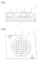
- FIG. 1 is a schematic cross-sectional view of a conductor bodies attached adhesive sheet according to a first embodiment of the present invention
- FIG. 2 is a schematic plane view of a conductor bodies attached adhesive sheet according to the same embodiment
- FIG. 3 is a schematic perspective view of when sticking the conductor bodies attached adhesive sheet according to the same embodiment and a semiconductor wafer
- FIG. 4 is a schematic cross-sectional view of a state where the conductor bodies attached adhesive sheet according to the same embodiment and a semiconductor wafer are stuck
- FIG. 5 is a schematic cross-sectional view of a state where an adhesive agent layer of the conductor bodies attached adhesive sheet according to the same embodiment and a substrate are aligned (furthermore, a state where the semiconductor wafer and the substrate are adhered).
- a conductor bodies attached adhesive sheet 1 comprises a base material 2, an adhesive agent layer 3 formed on the base material 2, and a plurality of conductor bodies 4 buried in the adhesive agent layer 3.
- the adhesive agent layer 3 has a same shape as that of a semiconductor wafer 5 shown in FIG. 3, which is a disk shape being formed a cut off portion (orientation flat). Note that the cut off portion may be a notch other than an orientation flat.
- each of the conductor bodies 4 is positioned on a front surface of the adhesive agent layer 3, and an lower end thereof is positioned on a back surface of the adhesive agent layer 3.
- the conductor bodies 4 buried in the adhesive agent layer 3 in the above way are arranged in a pattern corresponding to an arrangement of electrodes of a plurality of semiconductor integrated circuits formed on the semiconductor wafer 5 (FIG. 2).
- the adhesive agent layer 3 is comprised of an adhesive agent having gradable adhesiveness.
- the adhesive agents which exhibit gradable adhesiveness include those having a stage of tackiness (removable adhesiveness) and a stage of adhesiveness (a so-called tacky adhesive agent) and also include those which do not exhibit any tackiness/adhesiveness in a normal state but exhibit gradable tackiness/adhesiveness by a heat, compression or other triggers.
- the adhesive agent layer 3 preferably has a function as a so-called under filling material, that is, it is preferable to have a coefficient of linear expansion close to those of the semiconductor wafer 5 (or a semiconductor chip), substrate 6 and conductor bodies 4 when it finally hardens.
- An adhesive agent (tacky adhesive agent) of the former type may be, for example, a composition (a) containing a thermosetting resin and a tacky component, while an adhesive agent of the latter type may be, for example, a polyimide type resin (b) and an epoxy type resin (c), etc.
- the resins or the resin compositions may be used alone, or a material wherein the resin or the resin composition is used as a matrix can be also used. Note that a thickness of the adhesive agent layer 3 is normally determined in accordance with a height of the conductor bodies 4.
- thermosetting resin exhibits adhesiveness and the tacky component exhibits tackiness.
- thermosetting resin in such a composition include an epoxy resin, a phenol resin, an urea resin, a melanin resin, an unsaturated polyester resin, a resorcinol resin, a furan resin, a polyurethane resin, a silicone resin etc.
- An epoxy resin is preferable among them.
- examples of the tacky component include an acrylic type adhesive, a rubber type adhesive, a polyester type adhesive, or thermoplastic resins such as polyolefin, polyvinyl chloride, polystyrene, thermoplastic polyamide and polyester.
- a photopolymerizable composition may be included therein.
- a tacky component a (meth)acrylate copolymer is preferable.
- composition A a composition containing a thermoplastic resin and a tacky component
- composition A a composition containing a (meth)acrylate copolymer having a weight-average molecular weight of not less than 30000, an epoxy resin having a weight-average molecular weight of 100 to 10000, a photopolymerizable low molecular compound and thermal activation latent epoxy resin curing agent.
- the (meth)acrylate copolymer having a weight-average molecular weight of not less than 30000 may be a copolymer obtained by copolymerizing monomers, such as, (meth)acrylic acid, for example, alkyl (meth)acrylate derived from (meth)acrylic acid and alcohol having a carbon number of 1 to 14, hydroxyethyl (meth)acrylate, glycidyl (meth)acrylate, etc.
- a copolymer of (meth)acrylic acid and/or glycidyl (meth)acrylic acid and at least one kind of alkyl (meth)acrylate is preferable among them.
- alkyl (meth)acrylate derived from (meth)acrylic acid and alcohol having a carbon number of 1 to 14 examples include methyl (meth)acrylate, ethyl (meth)acrylate, butyl (meth)acrylate, etc.
- a content of a component unit derived from glycidyl (meth)acrylic acid in the copolymer is normally made to be 0 to 80 mol%, preferably 5 to 50 mol%, and a content of a component unit derived from (meth)acrylic acid is normally made to be 0 to 40 mol%, preferably 5 to 20 mol%.
- alkyl (meth)acrylate such as, methyl (meth)acrylate, ethyl (meth)acrylate, butyl (meth)acrylate, etc.
- An epoxy resin having a weight-average molecular weight of 100 to 10000 may be glycidyl ether of a phenol series, such as, bisphenol A, bisphenol F, resorcinol, phenyl novolac, cresol novolac; glycidyl ether of an alcohol series, such as, butanediol, polyethylene glycol, polypropylene glycol; glycidyl ether of carboxylic acid, such as, phthalic acid, isophthalic acid, tetrahydro phthalic acid; a glycidyl type or alkyl glycidyl type epoxy resin obtained by substituting active hydrogen bonded with nitrogen atom, such as aniline isocyanurate, with a glycidyl group; and so-called alicycle epoxide wherein an epoxy group is introduced by, for example, oxidizing carbon-carbon double bond in molecular, such as, vinyl cyclohexene epoxide, 3,4
- An epoxy equivalent weight of the above epoxy resins is preferably 50 to 5000 g/eq.
- the above epoxy resins may be used alone or by combining different kinds.
- bisphenol series glycidyl type epoxy resin, o-cresol novolac type epoxy resin and phenol novolac type epoxy resin are preferably used.
- the above epoxy resins are used in an amount of a range of normally 5 to 2000 parts by weight, preferably 100 to 1000 parts by weight with respect to 100 parts by weight of (meth)acrylate copolymer.
- a photopolymerizable low molecular compound is a compound able to be crosslinked by being irradiated an energy rays, such as, ultraviolet rays, electron rays, etc.
- an energy rays such as, ultraviolet rays, electron rays, etc.
- oligomer wherein there is at least one photopolymerizable double bond in molecular and a weight-average molecular weight (Mw) is in a range of 100 to 30000, preferably 300 to 10000 may be used.
- Example of a photopolymerizable low molecular compound may be urethane modified acrylate, epoxy modified acrylate, polyester acrylate, polyether acrylate; (meth)acrylic acid oligomer, itaconic acid oligomer and other oligomers having a functional group, such as hydroxy group or carboxyl group.
- Epoxy modified acrylate and urethane modified acrylate are preferably used among these.
- an upper limit of a weight-average molecular weight of the photopolymerizable low molecular compound is 30000 while that of the above (meth)acrylate copolymer is not less than 30000, and that the photopolymerizable low molecular compound always has at least one photopolymerizable double bond in its molecular while the above (meth)acrylate copolymer and epoxy resin normally do not have photopolymerizable double bond.
- the above photopolymerizable low molecular compound is used in an amount of a range of normally 10 to 1000 parts by weight, preferably 50 to 600 parts by weight with respect to 100 parts by weight of (meth)acrylate copolymer.
- a photopolymerizing initiator may be benzophenone, acetophenone, benzoin, benzoin alkyl ether, benzil, benzil dimethyl ketal, etc. These photopolymerizing initiators may be used alone or by combining different kinds. It is preferable to use ⁇ -substituted acetophenone among these.
- the above photopolymerizing initiator is used in an amount of a range of normally 0.1 to 10 parts by weight, preferably 1 to 5 parts by weight with respect to 100 parts by weight of a photopolymerizable low molecular compound.
- a thermal activation latent epoxy resin curing agent is a curing agent of a type that does not react with epoxy resins at a room temperature but activates by a heat of a certain temperature or more and reacts with epoxy resins.
- thermal activation latent epoxy resin curing agents there are those which generate active species (anion, cation) by a chemical reaction due to heating, those which are stably dispersed in an epoxy resin around a room temperature but become compatible and dissolved in an epoxy resin at a high temperature to start a curing reaction, those which are a type of curing agent contained in molecular sieves which is released at a high temperature to start a curing reaction, and those encapsulated in a micro-capsule, etc.
- These thermal activation latent epoxy resin curing agents can be used alone or by combining different kinds, and among these, it is preferable to use dicyanamide, imidazole compound, or a mixture of the dicyanamide and imidazole compound.
- thermal activation latent epoxy resin curing agents are used in an amount of a range of normally 0.1 to 40 parts by weight, preferably 1 to 30 parts by weight with respect to 100 parts by weight of an epoxy resin.
- thermo-curing agent such as polyisocyanate compound, other than the above thermal activation latent epoxy resin curing agents may be blended so as to change an adhesion ability of the compound A.
- the thermo-curing agent is used in an amount of a range of normally 0.1 to 30 parts by weight, preferably 5 to 20 parts by weight with respect to 100 parts by weight of (meth)acrylate copolymer.
- Examples of a polyimide type resin include a polyimide resin, a polyisoimide resin, maleimide resin, a bismaleimide resin, a polyamide-imide resin, a polyetherimide resin, a poly-imide-isoindoloquinazolinedioneimide resin, etc. These polyimide type resins may be used alone or by combining different kinds. It is preferable to use a polyimide resin among these. Furthermore, in polyimide resins, there are thermoplastic polyimide resins which do not have a reactive functional group and thermosetting polyimide resins which show an imidation reaction by heating. Any of these may be used or the both may be mixed to be used.
- a weight-average molecular weight of polyimide type resins is preferably about 10,000 to 1,000,000, particularly about 50,000 to 100,000.
- the weight-average molecular weight is preferably about 100 to 100,000.
- the above resins or resin compositions may be blended additives, such as, a leuco dye, an antistatic agent, a coupling agent, an ion scavenger and a copper inhibitor, and other polymers, oligomers and low molecular compounds, etc.
- additives such as, a leuco dye, an antistatic agent, a coupling agent, an ion scavenger and a copper inhibitor, and other polymers, oligomers and low molecular compounds, etc.
- 3-[N-(P-tolylamino)-7-anilinofluoran, 4,4',4"-trisdimethylamino triphenylmethane, etc. may be used, and as an antistatic agent, carbon black, anion type and cation type surface-active agents, etc. may be used.
- polymers, oligomers and low molecular compounds may be, for example, a variety of polymers or oligomers, such as, an epoxy resin, an amide resin, an urethane resin, an amide acid resin, a silicone resin, an acrylic resin and acrylic rubber; and nitrogen-contained organic compounds, such as, triethanolamine, ⁇ , ⁇ -(bis3-aminopropyl) polyethylene glycol ether.
- polymers or oligomers such as, an epoxy resin, an amide resin, an urethane resin, an amide acid resin, a silicone resin, an acrylic resin and acrylic rubber
- nitrogen-contained organic compounds such as, triethanolamine, ⁇ , ⁇ -(bis3-aminopropyl) polyethylene glycol ether.
- those which have the above linear expansion coefficient when finally hardened may be selected as an adhesive agent constituting the adhesive agent layer 3, and it is also possible to make a material have the above linear expansion coefficient when it is finally hardened by adding an inorganic filler, etc. to the adhesive agent as a matrix.
- An inorganic filler may be a fused silica, crystal silica, almina, boron nitride, aluminum nitride, silicon nitride, magnesia, magnesium silicate, etc., and ones being spherical are preferable.
- a blending amount and particle diameter of an inorganic filler with respect to a matrix may be suitably adjusted and selected so that the adhesive agent layer 3 has a desired linear expansion coefficient and is not restrained in terms of fluidity as in an under filling agent of the related art.
- a photopolymerizable low molecular compound in the composition A can be efficiently polymerized by irradiating a light.
- Any material would be basically sufficient as a base material 2 in the present embodiment as far as it supports the adhesive agent layer 3 and is able to be removed from the adhesive agent layer 3, and it may also have stiffness.
- the base material 2 examples include films made by resins, such as, polyethylene, polypropylene, polybutene, polybutadiene, vinyl chloride, ionomer, ethylene-methacrylic acid copolymer, polyethylene terephthalate, polyethylene naphthalate, polybutylene terephthalate, polyimide, polyetherimide, polyaramide, polyetherketone, polyether ether ketone, polyphenylene sulfide, poly (4-methylpentene-1), polytetrafluoroethylene, and those obtained by crosslinking these resins. These films may be used alone or by laminating different kinds. A film thickness thereof is normally about 10 to 300 ⁇ m, preferably 20 to 150 ⁇ m.
- resins such as, polyethylene, polypropylene, polybutene, polybutadiene, vinyl chloride, ionomer, ethylene-methacrylic acid copolymer, polyethylene terephthalate, polyethylene naphthalate, polybutylene
- papers such as, a glassine paper, clay coated paper, resin coated paper, a laminated paper (polyethylene laminated paper, polypropylene laminated paper, etc.) or nonwoven fabrics, metallic foils, etc. may be used.
- a surface tension of a surface of the base material 2 on which the adhesive agent layer 3 is formed is preferably not more than 40 dyn/cm.
- Release treating may be performed on the surface of the base material 2 on which the adhesive agent layer 3 is formed to adjust the surface tension to be a preferable value.
- Alkyd resin type, silicone resin type, fluorine resin type, unsaturated polyester resin type, polyolefin resin type and wax type releasing agents, etc. may be used for the release treating. Note that when the base material 2 itself has the above surface tension, the base material 2 can be used as it is without any release treating.
- composition A for the adhesive agent layer 3
- a material wherein an energy rays to be irradiated on the composition A can permeate it is particularly preferable to use a material having a low adhesiveness to the composition A having improved tackiness due to the energy rays irradiation.
- a fusing point of the heat resistance resin is preferably not less than 230°C, more preferably 250 to 300°C, and particularly preferably 260 to 280°C.
- dicing of a semiconductor wafer can be also performed. In this case, spaces between semiconductor chips may be made wider by expanding the base material 2 after dicing.
- the base material 2 able to be expanded in this way it is preferable to select a resin film having a extensible property in the length and width directions and a Young's modulus of 1.0 x 10 4 kg/cm 2 or less.
- the conductor bodies 4 are not particularly limited as far as it is normally used as bumps (electrodes) in a semiconductor device.
- a material of the conductor bodies 4 metals or alloys of solder, Au, Cu, Ni, Ag, Pt, etc., resins plated by these metals or alloys, resins wherein conductive powder is dispersed, conductive resins, etc. is normally selected.
- a shape of the conductor bodies 4 is sphere, but it is not limited to this and may have a columnar shape, prismatic shape or conical shape, etc.
- the conductor bodies 4 may be such a shape from the beginning or may be made to be the spheric shape or other shape by being printed a conductive paste.
- a height of the conductor bodies 4 is normally 50 to 300 ⁇ m, but it may be less than 50 ⁇ m, or furthermore, 30 ⁇ m or less. In the present embodiment, the height of the conductor bodies 4 is the same as the thickness of the adhesive agent layer 3.
- a pattern of the conductor bodies 4 in the present embodiment is a pattern corresponding to a so-called area type semiconductor chip on which electrodes are formed all over the chip, but the present invention is not limited to this pattern. It may be a pattern corresponding to a so-called peripheral type semiconductor chip wherein electrodes are formed around the chip.
- a process for producing the above a conductor bodies attached adhesive sheet 1 is not particularly limited, but generally, after printing conductor bodies 4 by a predetermined pattern on the base material 2, an adhesive agent is coated to form the adhesive agent layer 3 on the base material 2.
- an adhesive agent is coated to form the adhesive agent layer 3 on the base material 2.
- screen printing or a process for injecting the conductor bodies 4 by an ink-jet method, etc. are applied.
- a method of coating the adhesive agent screen process printing, roll coating, knife coating and micro-die methods, etc. are applied.
- a solvent wherein respective components of the adhesive agent can be uniformly dissolved and dispersed can be also used.
- the solvent is not particularly limited as far as it is capable of uniformly dissolving and dispersing the respective components therein.
- the solvent include dimethylformamide, dimethylacetoamide, N ⁇ methylpyrrolidone, dimethyl sulfoxide, diethylene glycol dimethyl ether, toluene, benzene, xylene, methyl ethyl ketone, tetrahydrofuran, ethyl-cellosolve, dioxane, cyclopentanone, cyclohexanone, monoglyme, etc. These solvents can be used alone or by being mixed with different kinds.
- the above conductor bodies attached adhesive sheet 1 may be produced by forming the adhesive agent layer 3 by coating an adhesive agent on the base material 2, then burying the conductor bodies 4 in the adhesive agent layer 3 in a predetermined pattern.
- a method of burying the conductor bodies 4 a method of pressing one obtained by forming the conductor bodies 4 on a sheet or adsorbing the conductor bodies 4 on a jig in a predetermined pattern and one obtained by forming the adhesive agent layer 3 on a sheet so as to bury the conductor bodies 4 in the adhesive agent layer 3, a method of process injecting the conductor bodies 4 to the adhesive agent layer 3 by an ink-jet method, etc. may be applied.
- the conductor bodies 4 may be buried in the adhesive agent.
- the upper end and the lower end of the conductor bodies 4 may be positioned on the front surface and back surface of the adhesive agent layer 3 by pressing at the time of adhering a protective film.
- a plurality of adhesive agent layers 3 may be formed by being set beside each other on one base material 2.
- a semiconductor wafer 5 is put on the adhesive agent layer 3 of the conductor bodies attached adhesive sheet 1 and the two are stuck to each other.
- the semiconductor wafer 5 is aligned so that an electrodes 51 of a semiconductor integrated circuit formed on the semiconductor wafer 5 and the conductor bodies 4 can be electrically connected, and the semiconductor wafer 5 and the adhesive agent layer 3 of the conductor bodies attached adhesive sheet 1 are stuck to each other.
- the electrodes 51 of the semiconductor wafer 5 and the conductor bodies 4 can be electrically connected by sticking the aligned semiconductor wafer 5 to the adhesive agent layer 3.
- the electrodes 51 of the semiconductor wafer 5 may be those called bonding pads or conductor bodies pads, and may be barrier metal formed thereon, furthermore, pillars.
- the above sticking can be attained by an adhesion force of the tackiness.
- the adhesive agent layer 3 does not have any tackiness, it is preferable to stick the adhesive agent layer 3 and the semiconductor wafer 5 by hot pressing.
- the heating temperature of the hot pressing is preferably about 30 to 300°C, particularly preferably about 50 to 200°C, the heating time is preferably about 1 second to 10 minutes, particularly preferably about 1 to 30 seconds, and the pressure is preferably about 1 to 10 kg/cm 2 , particularly preferably about 1 to 5 kg/cm 2 .
- dicing of the semiconductor wafer 5 may be performed if needed. At this time, dicing may be performed by additionally preparing a wafer dicing sheet, removing the base material 2 from the conductor bodies attached adhesive sheet 1 and sticking the wafer dicing sheet to the adhesive agent layer 3 of the conductor bodies attached adhesive sheet 1, or by without using a wafer dicing sheet as such.
- spaces between semiconductor chips may be made wide by expanding in accordance with need.
- the wafer dicing sheet can be expanded, and even when such a wafer dicing sheet is not used, if a base material 2 able to be expanded is used, the base material 2 may be expanded.
- the adhesive agent layer 3 of the conductor bodies attached adhesive sheet 1 when using the above composition A for the adhesive agent layer 3 of the conductor bodies attached adhesive sheet 1, it is preferable to irradiate an energy rays from the base material 2 side of the conductor bodies attached adhesive sheet 1 to the adhesive agent layer 3.
- the energy rays ultraviolet rays having a center wavelength of about 365 nm and electron rays, etc. may be used.
- the illuminance is set in a range of 20 to 500 mW/cm 2 and the irradiation time is set in a range of 0.1 to 150 seconds.
- the irradiation time is set in a range of 0.1 to 150 seconds.
- conditions can be set conforming to the case of ultraviolet rays.
- heating may be also auxiliary performed at the time of irradiating the above energy rays.
- an adhesion force between the semiconductor wafer 5 (or a semiconductor chip) and the adhesive agent layer 3 is normally improved to 50 to 4000 g/25mm, preferably 100 to 3000 g/25mm.
- an adhesion force between the adhesive agent layer 3 and the base material 2 normally declines to 1 to 500 g/25mm, preferably 100 g/25mm or less.
- the base material 2 is removed from the above adhesive agent layer 3 of the conductor bodies attached adhesive sheet 1.
- the base material 2 can be surely removed while leaving the adhesive agent layer 3 fixed on the semiconductor wafer 5 (or a semiconductor chip) side. Note that the irradiation of the energy rays may be performed before a dicing process.
- alignment (superimposition) of the semiconductor wafer 5 (or a semiconductor chip) with a substrate 6 is performed so that electrodes 61 formed on the substrate 6 and conductor bodies 4 are electrically connected.
- the conductor bodies 4 and the electrodes 61 of the substrate 6 can be electrically connected by the aligning of the semiconductor wafer 5 (or a semiconductor chip).
- the semiconductor wafer 5 (or a semiconductor chip) and the substrate 6 are adhered via the adhesive agent layer 3.
- the adhesion process can be generally performed by heating. The heating is preferably performed during superimposing the substrate 6 and the semiconductor wafer 5 (or a semiconductor chip) or immediately after the superimposition. At this time, when the adhesive agent layer 3 does not have any tackiness, a temporary adhesion is preferably performed before an actual adhesion.
- a heating temperature of the temporary adhesion is normally 100 to 300°C, preferably 150 to 250°C, a heating time is normally 1 second to 10 minutes, preferably 1 to 30 seconds, while a heating temperature of the actual adhesion is normally 100 to 300°C, preferably 150 to 250°C and a heating time is normally 1 to 120 minutes, preferably 1 to 60 minutes.
- the semiconductor wafer 5 (or a semiconductor chip) and the substrate 6 may be pressed to adhere by applying a suitable pressure in the thickness direction of a laminate formed by the semiconductor wafer 5 (or a semiconductor chip), the adhesive agent layer 3, and the substrate 6.
- electrodes 51 of the semiconductor wafer 5 (or a semiconductor chip) and the conductor bodies 4 can be surely connected and the conductor bodies 4 and the electrodes 61 of the substrate 6 can be surely connected.
- the pressing is particularly efficient in the case where an upper end and/or lower end of the conductor bodies 4 is not appeared on the surface of the insulative adhesive agent layer 3 in the conductor bodies attached adhesive sheet 1.
- the conductor bodies 4 when a fusing point of the conductor bodies 4 is lower than the above heating temperature, for example when the conductor bodies 4 are made of solder balls or a resin, the conductor bodies 4 are fused or soften to deform in some cases.
- the result obtained by adhering the semiconductor wafer 5 and the substrate 6 may be cut and chipped to be a semiconductor device 7, or those in a wafer size may be used as semiconductor devices 7 without cutting. Cutting can be performed by a dicing saw and other normal cutting means. Thus cut results become so-called real chip size package type semiconductor devices.
- a conductor bodies attached adhesive sheet 1 was stuck to a semiconductor wafer 5 and then a substrate 6 was adhered thereto, but the present invention is not limited to this.
- the conductor bodies attached adhesive sheet 1 may be adhere to the substrate 6 and then the semiconductor wafer 5 is adhered thereto.
- the conductor bodies 4 are buried in the adhesive agent layer 3 in advance and the adhesive agent layer 3 serves as an under filling material, a process of injecting an under filling material to a space between the semiconductor wafer 5 (or a semiconductor chip) and the substrate 6 becomes unnecessary. Accordingly, any defects caused by fluidity of an under filling material does not exist in thus obtained semiconductor device 7.
- Figure 6 is a schematic perspective view of when sticking the conductor bodies attached adhesive sheet according to the second embodiment of the present invention and a semiconductor chip.
- a conductor bodies attached adhesive sheet 1A according to the second embodiment comprises, as same as the conductor bodies attached adhesive sheet 1 according to the first embodiment, a base material 2A, an adhesive agent layer 3A formed on the base material 2A, and a plurality of conductor bodies 4A buried in the adhesive agent layer 3A, but differs from the conductor bodies attached adhesive sheet 1 according to the first embodiment in the point that the adhesive agent layer 3A is formed to be a same shape as that of a semiconductor chip 52.
- the conductor bodies 4A buried in the adhesive agent layer 3A are arranged in a pattern corresponding to an arrangement of electrodes of a semiconductor integrated circuit formed on the semiconductor chip 52.
- the conductor bodies attached adhesive sheet 1A according to the second embodiment can be produced in a similar process to in the conductor bodies attached adhesive sheet 1 according to the first embodiment, and a plurality of adhesive agent layers 3 may be formed by being set beside each other on one base material 2A.
- a semiconductor device in the case of producing a semiconductor device by using the conductor bodies attached adhesive sheet 1A according to the second embodiment, a semiconductor device can be produced in a similar process to in the conductor bodies attached adhesive sheet 1 according to the first embodiment except that a dicing process and a process of cutting a result obtained by adhering the semiconductor wafer and the substrate are unnecessary.
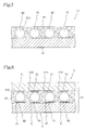
- FIG. 7 is a schematic sectional view of the conductor bodies attached adhesive sheet according to the third embodiment
- FIG. 8 is a schematic sectional view of a state where a semiconductor wafer and a substrate are adhered via an adhesive agent layer of the conductor bodies attached adhesive sheet according to the third embodiment.
- a conductor bodies attached adhesive sheet 1B comprises a base material 2B, an adhesive agent layer 3B formed on the base material 2B and a plurality of conductor bodies 4B buried in the adhesive agent layer 3B.
- An upper end of each of the plurality of conductor bodies 4B in the present embodiment is positioned lower than a surface of the adhesive agent layer 3B (actually buried in the adhesive agent layer 3B) and a lower end of each of the conductor bodies 4B is positioned on a back surface of the adhesive agent layer 3B.
- the present invention is not limited to this and the lower ends of the conductor bodies may positioned upper than the back surface of the adhesive agent layer 3B and the upper ends thereof may be positioned on the surface of the adhesive agent layer 3B. Alternately, the conductor bodies 4B may be completely buried in the adhesive agent layer 3B.
- the adhesive agent layer 3B in the present embodiment has anisotropic conductivity, that is, it exhibits conductivity in the thickness direction when being pressed in the thickness direction, but has an insulation property in the surface direction.
- conductive particles 31B are dispersed in an insulative matrix in the adhesive agent layer 3B.
- conductive particles 31B particles made of a metal having an excellent conductivity, such as Ni, Ag, Au, Cu, solder, etc., polymer particles covered with the metals, or these metal particles or metal covered particles on which an extremely thin organic insulation layer is formed so as to improve the insulation property in the surface direction may be used.
- a metal having an excellent conductivity such as Ni, Ag, Au, Cu, solder, etc.
- polymer particles covered with the metals or these metal particles or metal covered particles on which an extremely thin organic insulation layer is formed so as to improve the insulation property in the surface direction may be used.
- an average particle diameter of the conductive particles 31B is preferably 1 to 100 ⁇ m, and a dispersion amount of the conductive particles 31B is preferably 1 to 30 vol% with respect to the matrix.
- the conductor bodies attached adhesive sheet 1B according to the third embodiment can be produced in a similar process to in the conductor bodies attached adhesive sheet 1 according to the first embodiment. Also, when producing a semiconductor device by using the conductor bodies attached adhesive sheet 1B according to the third embodiment, it can be produced in a similar process to in the conductor bodies attached adhesive sheet 1 according to the first embodiment except for applying a suitable pressure in the thickness direction of the semiconductor wafer 5 (or a semiconductor chip) and the adhesive agent layer 3B and letting conductivity appear in the thickness direction of the adhesive agent layer 3B.
- electrodes 51 of the semiconductor wafer 5 (or a semiconductor chip) and electrodes 61 of the base material 6 are electrically connected via the conductor bodies 4B and conductive particles 31B.
- the base materials 2, 2A and 2B may have the same shape as that of the adhesive agent layers 3, 3A and 3B.
- the present invention is useful in producing a semiconductor device having no defects caused by fluidity of an under filling material.
- a copolymer having an weight average molecular weight of 900,000 was prepared by copolymerizing 55 parts by weight of butyl acrylate, 10 parts by weight of methyl methacrylate, 20 parts by weight of glycidyl methacrylate and 15 parts by weight of 2-hydroxyethyl acrylate.
- a composition A was obtained by mixing 10 parts by weight of the above copolymer, 24 parts by weight of liquid bisphenol A type epoxy resin (Epikote 828 produced by Yuka Shell Epoxy Co., Ltd), 10 parts by weight of o-cresol novolac type epoxy resin (EOCN-104S produced by NIPPON KAYAKU Co., Ltd.), 0.05 part by weight of e-glycidoxypropyltrimethoxysilane as a coupling agent, 1.5 part by weight of dicyandiamide as a thermal activation latent curing agent, 1.5 part by weight of 2-phenyl-4,5-hydroxymethylimidazole, 5 parts by weight of urethane acrylate type oligomer (Seikabeam 14-29B produced by Dainichiseika Color & Chemicals Mfg.Co.,Ltd.) as a photopolymerizable low molecular compound, 0.2 part by weight of 1-hydroxycyclohexyl phenyl ketone as a photopol
- Spheric conductor bodies having a diameter of 200 ⁇ m were formed in the same arrangement of electrodes of a semiconductor integrated circuit by using as a release film a polyethylene terephthalate (PET) film having a thickness of 38 ⁇ m, one surface of which was releasing treated by a silicone resin, and by printing a conductive paste (DW-250H-5 produced by TOYOBO Co.,Ltd.) on the releasing treated surface of the release film by screen printing.
- PET polyethylene terephthalate
- composition A was coated by screen printing and dried at 100°C for 5 minutes to form an adhesive agent layer, a polyethylene film (thickness: 100 ⁇ m, surface tension: 36 dyn/cm) was stuck as a base material on the surface of the adhesive agent layer, and a conductor bodies attached adhesive sheet wherein a thickness of an adhesive agent layer was 200 ⁇ m was obtained.
- the conductor bodies attached adhesive sheet was made to be a wafer form by punching. Also, a conductor bodies attached adhesive sheet of a chip size was prepared separately in a similar way.
- Adhesive agent polyimide type resin
- Spheric conductor bodies having a diameter of 200 ⁇ m were formed in the same arrangement of electrodes of a semiconductor integrated circuit by using as a base material polyethylene naphthalate (PEN) film (thickness: 25 ⁇ m, surface tension: 34 dyn/cm), one surface of which was releasing treated by a silicon resin, and by printing a conductive paste (DW-250H-5 produced by TOYOBO Co.,Ltd.) on the releasing treated surface of the base material by screen printing.
- PEN polyethylene naphthalate
- thermoplastic polyimide Upitite UPA-N221 produced by Ube Industries Ltd.
- a conductor bodies attached adhesive sheet was obtained.
- Adhesive agent epoxy type resin composition
- An epoxy type resin adhesive agent was prepared by mixing 40 parts by weight of a high molecular bisphenol type epoxy resin (Epikote 1010 produced by Yuka Shell Epoxy Co.,Ltd), 20 parts by weight of a multifunctional cresol novolac type epoxy resin (EOCN-4600 produced by Nippon Kayaku Co.,Ltd.), 1.5 parts by weight of 2-phenyl-4,5-hydroxymethylimidazole as a thermal activation latent curing agent, and 0.1 part by weight of ⁇ -glycidepropyltrimethoxysilane.
- a high molecular bisphenol type epoxy resin Epikote 1010 produced by Yuka Shell Epoxy Co.,Ltd
- EOCN-4600 produced by Nippon Kayaku Co.,Ltd.
- suction was performed from a back surface of a jig having holes in the same arrangement as that of electrodes of a semiconductor integrated circuit so as to adsorb solder balls (Pb-63Sn) having a diameter of 200 ⁇ m as conductor bodies into respective holes to be made aligned.
- the conductor bodies were buried in the adhesive agent layer. Then, the adhesion agent layer was dried at 100°C for 5 minutes so that a conductor bodies attached adhesion sheet wherein a thickness of the adhesive agent layer was 200 ⁇ m was obtained.
- Adhesive agent anisotropic conductive adhesive agent
- thermosetting resin which is obtained by mixing a hundred parts by weight of bisphenol A type epoxy resin (RE-310S produced by Nippon Kayaku Co.,Ltd.), 20 parts by weight of a first curing agent (Cureduct P-0505 produced by Shikoku Chemicals Corp.) and 10 parts by weight of second curing agent (Cureduct L-01B produced by Shikoku Chemicals Corp.) as an imidazole series adduct type latent curing agent to prepare an anisotropic conductive adhesive agent.
- bisphenol A type epoxy resin RE-310S produced by Nippon Kayaku Co.,Ltd.
- first curing agent Cureduct P-0505 produced by Shikoku Chemicals Corp.
- second curing agent Cureduct L-01B produced by Shikoku Chemicals Corp.
- a conductor bodies attached adhesive sheet was prepared in a similar way to in the example 3 except that the above anisotropic conductive adhesive agent was used as an adhesive agent.
- a conductor bodies attached adhesive sheet in a wafer shape prepared in the example 1 (wherein an adhesive agent layer was exposed by removing a PET film as a release film. The following will be the same.) and a semiconductor wafer were aligned so that the conductor bodies of the conductor bodies attached adhesive sheet were electrically connected to electrodes of a semiconductor integrated circuit formed on the semiconductor wafer, and the conductor bodies attached adhesive sheet was stuck to the semiconductor wafer. They were fixed to a ring frame.
- a conductor bodies attached adhesive sheet prepared in the example 2 and a semiconductor wafer were aligned so that conductor bodies of the conductor bodies attached adhesive sheet was electrically connected to electrodes of semiconductor integrated circuit formed on the semiconductor wafer.
- the two were hot-pressed at 180°C by 5 kg/cm 2 for 30 seconds, then, the above conductor bodies attached adhesive sheet was cut along a semiconductor wafer shape.
- the PEN film as a base material of the above conductor bodies attached adhesive sheet was removed from the adhesive agent layer, then a separately prepared wafer dicing sheet (ADWILL G-11 produced by Lintec Corporation) was stuck to the adhesive agent layer, and the adhesive agent layer attached semiconductor wafer was fixed on a ring frame.
- ADWILL G-11 produced by Lintec Corporation
- the conductor bodies attached adhesive sheet prepared in the example 3 and a semiconductor wafer were aligned so that the conductor bodies of the conductor bodies attached adhesive sheet were electrically connected to electrodes of a semiconductor integrated circuit formed on the semiconductor wafer.
- the two were hot-pressed at 140°C by 5 kg/cm 2 for 30 seconds, then the above conductor bodies attached adhesive sheet was cut along a semiconductor wafer shape.
- the PET film as a base material of the above conductor bodies attached adhesive sheet was removed from the adhesive agent layer, then a separately prepared wafer dicing sheet (ADWILL G-11 produced by Lintec Corporation) was stuck to the adhesive agent layer, and the adhesive agent layer attached semiconductor wafer was fixed on a ring frame.
- ADWILL G-11 produced by Lintec Corporation
- Full-cut dicing was performed in a similar way to in the example 6 and thus obtained adhesive agent layer attached chip was picked up. After that, the conductor bodies of the adhesive agent layer and the electrodes on the substrate were aligned, the chip and the substrate were temporarily adhered by heating at 180°C by 5 kg/cm 2 for 5 seconds, then furthermore heated at 180°C for 60 minutes to firmly adhere the chip and the substrate via the above adhesive agent layer so as to obtain a semiconductor device.
- the conductor bodies attached adhesive sheet prepared in the example 4 and a semiconductor wafer were aligned so that the conductor bodies of the conductor bodies attached adhesive sheet were electrically connected to electrodes of a semiconductor integrated circuit formed on the semiconductor wafer. After the two were hot-pressed at 150°C by 5 kg/cm 2 for 30 seconds, the above conductor bodies attached adhesive sheet was cut along the semiconductor wafer shape.
- an adhesive agent layer attached chip was obtained in a similar way to in the example 7.
- the conductor bodies of the adhesive agent layer and the electrodes on the substrates were aligned.
- the chip and the substrate were temporarily adhered by heating at 150°C by 5 kg/cm 2 for 5 seconds, then furthermore heated at 180°C for 60 minutes to firmly adhere the chip and the substrate via the above adhesive agent layer so as to obtain a semiconductor device.
- the conductor bodies attached adhesive sheet in a wafer shape prepared in the example 1 and a semiconductor wafer were aligned so that the conductor bodies of the conductor bodies attached adhesive sheet were electrically connected to the electrodes of a semiconductor integrated circuit formed on the semiconductor wafer, and a conductor bodies attached adhesive sheet was stuck to the semiconductor wafer.
- a polyethylene film as a base material was removed from the adhesive agent layer and the conductor bodies of the adhesive agent layer and the electrodes on the substrate were aligned. After temporarily adhering the semiconductor wafer and the substrate by heating at 150°C by 5 kg/cm 2 for 5 seconds, they were furthermore heated at 160°C for 60 minutes to firmly adhere the semiconductor wafer and the substrate via the above adhesive agent layer.
- a separately prepared ultraviolet ray curing type wafer dicing sheet (ADWILL D-510T produced by Lintec Corporation) was stuck to the above substrate, and the substrate attached semiconductor wafer was fixed to the ring frame. Then full-cut dicing was performed in a similar way to in the example 6. After ultraviolet rays were irradiated to the above ultraviolet ray curing type wafer dicing sheet, thus obtained substrate attached chip was picked up so as to obtain a semiconductor device.
- the conductor bodies attached adhesive sheet in a wafer shape prepared in the example 1 and a substrate were aligned so that the conductor bodies of the conductor bodies attached adhesive sheet were electrically connected to electrodes on the substrate, and the conductor bodies attached adhesive sheet was stuck to the substrate.
- a polyethylene film as a base material was removed from the adhesive agent layer, and the conductor bodies of the adhesive agent layer and the electrodes of the semiconductor integrated circuit formed on the semiconductor wafer were aligned. After temporarily adhering the substrate and the semiconductor wafer by heating at 150°C by 5 kg/cm 2 for 5 seconds, they were furthermore heated at 160°C for 60 minutes to firmly adhere the substrate and the semiconductor wafer via the above adhesive agent layer.
- a separately prepared ultraviolet ray curing type wafer dicing sheet (ADWILL D-510T produced by Lintec Co.,Ltd.) was stuck to the above substrate, and the substrate attached semiconductor wafer was fixed on the ring frame. Then full-cut dicing is performed in a similar way to in the example 6. After ultraviolet rays were irradiated to the above ultraviolet ray curing type wafer dicing sheet, thus obtained substrate attached chip is picked up so as to obtain a semiconductor device.
- the conductor bodies attached adhesive sheet in a wafer shape produced in the example 1 and a substrate were aligned so that the conductor bodies of the conductor bodies attached adhesive sheet were electrically connected to the electrodes on the substrate.
- the conductor bodies attached adhesive sheet was stuck to the substrate, and the two were fixed on the ring frame.
- Full-cut dicing was performed on the adhesive agent layer attached substrate in a similar way to in the example 5. After ultraviolet rays were irradiated to the adhesive agent layer, a polyethylene film as a base material of the conductor bodies attached adhesive sheet was expanded, and an obtained adhesive agent attached substrate was picked up. After that, conductor bodies of the adhesive agent layer and electrodes of a separately diced semiconductor chip were aligned. The substrate and the semiconductor chip were temporarily adhered at 150°C by 5 kg/cm 2 for 5 seconds, then furthermore heated at 160°C for 60 minutes to firmly adhere the substrate and the semiconductor chip via the above adhesive agent layer.
- the conductor bodies attached adhesive sheet of a chip size prepared in the example 1 and a separately diced semiconductor chip were aligned so that the conductor bodies of the conductor bodies attached adhesive sheet were electrically connected to electrodes of the semiconductor chip, and the conductor bodies attached adhesive sheet was stuck to the semiconductor chip.
- a polyethylene film as a base material was removed from the adhesive agent layer, and the conductor bodies in the adhesive agent layer and the electrodes on the substrates were aligned.
- the semiconductor chip and the substrate were temporarily adhered at 150°C by 5 kg/cm 2 for 5 seconds, then, furthermore heated at 160°C for 60 minutes to firmly adhere the semiconductor chip and the substrate via the above adhesive agent layer.
- the conductor bodies attached adhesive sheet of a chip size prepared in the example 1 and a substrate were aligned so that the conductor bodies of the conductor bodies attached adhesive sheet were electrically connected to electrodes on the substrate, and the conductor bodies attached adhesive sheet was stuck to the substrate.
- a polyethylene film as a base material was removed from the adhesive agent layer, and the conductor bodies of the adhesive agent layer and electrodes of a separately diced semiconductor chip were aligned.
- the substrate and the semiconductor chip were temporarily adhered by heating at 150°C by 5 kg/cm 2 for 5 seconds, then, furthermore heated at 160°C for 60 minutes to firmly adhere the substrate and the semiconductor chip via the above adhesive agent layer.
- a Pressure Cooker Test was conducted on the semiconductor devices obtained in the examples 5 to 13 under conditions of 121°C, 100 %RH, 2 atmospheres and 168 hours. AS a result, no cracks and the like occurred in any of the semiconductor devices.
Landscapes
- Chemical & Material Sciences (AREA)
- Organic Chemistry (AREA)
- Adhesives Or Adhesive Processes (AREA)
- Adhesive Tapes (AREA)
- Wire Bonding (AREA)
Abstract
Description

Claims (11)
- A conductor bodies attached adhesive sheet, comprising a base material, an adhesive agent layer formed on said base material and conductor bodies buried in said adhesive agent layer in an arrangement corresponding to electrodes of a semiconductor integrated circuit and electrodes of a substrate, wherein an adhesive agent constituting said adhesive agent layer has gradable adhesiveness.
- The conductor bodies attached adhesive sheet as set forth in claim 1, wherein upper ends and/or lower ends of said conductor bodies are substantially positioned on a front surface and/or a back surface of said adhesive agent layer.
- The conductor bodies attached adhesive sheet as set forth in claim 1 or 2, wherein said conductor bodies attached adhesive sheet is made to be a size corresponding to a semiconductor wafer, and said conductor bodies are arranged so as to correspond to electrodes of a plurality of semiconductor integrated circuit formed on said semiconductor wafer.
- A process for producing a semiconductor device, comprising the steps of;sticking a semiconductor chip or a semiconductor wafer and said conductor bodies attached adhesive sheet as set forth in any of claims 1 to 3 so that electrodes of a semiconductor integrated circuit formed on said semiconductor chip or semiconductor wafer and the conductor bodies of said adhesive sheet can be electrically connected;removing the base material from the adhesive agent layer of said conductor bodies attached adhesive sheet; andaligning said adhesive agent layer with a substrate so that the conductor bodies buried in said adhesive agent layer and electrodes of said substrate can be electrically connected, and adhering said semiconductor chip or semiconductor wafer and said substrate.
- A process for producing a semiconductor device, comprising the steps of;sticking a substrate and said conductor bodies attached adhesive sheet as set forth in any one of claims 1 to 3 so that electrodes of said substrate and the conductor bodies of said adhesive sheet can be electrically connected;removing the base material from the adhesive agent layer of said conductor bodies attached adhesive sheet; andaligning a semiconductor chip or a semiconductor wafer with said adhesive agent layer so that electrodes of a semiconductor integrated circuit formed on said semiconductor chip or semiconductor wafer and the conductor bodies buried in said adhesive agent layer can be electrically connected, and adhering said substrate and said semiconductor chip or semiconductor wafer.
- A process for producing a semiconductor device, comprising the steps of;sticking a semiconductor wafer and said conductor bodies attached adhesive sheet as set forth in claim 3 so that electrodes of a semiconductor integrated circuit formed on said semiconductor wafer and the conductor bodies of said adhesive sheet can be electrically connected;removing the base material from the adhesive agent layer of said conductor bodies attached adhesive sheet;aligning said adhesive agent layer with a substrate so that the conductor bodies buried in said adhesive agent layer and electrodes of said substrate can be electrically connected, and adhering said semiconductor wafer and said substrate; andcutting a laminate obtained by adhering said semiconductor wafer and said substrate to obtain a semiconductor device.
- A process for producing a semiconductor device, comprising the steps of;sticking a substrate and said conductor bodies attached adhesive sheet as set forth in claim 3 so that electrodes of said substrate and the conductor bodies of said adhesive sheet can be electrically connected;removing the base material from the adhesive agent layer of said conductor bodies attached adhesive sheet;aligning a semiconductor wafer with the adhesive agent layer so that electrodes of semiconductor integrated circuit formed on said semiconductor wafer and the conductor bodies buried in said adhesive agent layer can be electrically connected, and adhering said substrate and said semiconductor wafer; andcutting a laminate obtained by adhering said substrate and said semiconductor wafer to obtain a semiconductor device.
- A process for producing a semiconductor device, comprising the steps of;sticking a semiconductor wafer and said conductor bodies attached adhesive sheet as set forth in claim 3 so that electrodes of a semiconductor integrated circuit formed on said semiconductor wafer and the conductor bodies of said adhesive sheet can be electrically connected;cutting said semiconductor wafer together with the adhesive agent layer of said conductor bodies attached adhesive sheet to obtain semiconductor chips;expanding spaces between said semiconductor chips if needed;removing the adhesive agent layer attached semiconductor chip from the base material of said conductor bodies attached adhesive sheet; andaligning said adhesive agent layer with a substrate so that the conductor bodies buried in said adhesive agent layer and electrodes of said substrate can be electrically connected, and adhering said semiconductor chip and said substrate.
- The process for producing a semiconductor device as set forth in any one of claims 4 to 8, further comprising a step of relatively improving an adhesion force of said adhesive agent layer to said semiconductor chip, semiconductor wafer or substrate than an adhesion force of said adhesive agent layer to said base material before the step of removing the base material from the adhesive agent layer of said conductor bodies attached adhesive sheet.
- A semiconductor device produced by said process as set forth in any one of claims 4 to 9.
- A semiconductor device, comprising a semiconductor chip, a substrate adhered to said semiconductor chip via an adhesive agent layer, and conductor bodies for electrically connecting electrodes of a semiconductor integrated circuit formed on said semiconductor chip and electrodes of said substrate in said adhesive agent layer,
wherein said adhesive agent layer is obtained by hardening a layer of an adhesive agent wherein said conductor bodies are buried.
Applications Claiming Priority (2)
| Application Number | Priority Date | Filing Date | Title |
|---|---|---|---|
| JP2001099019A JP2002299378A (en) | 2001-03-30 | 2001-03-30 | Adhesive sheet with conductor, semiconductor device manufacturing method and semiconductor device |
| JP2001099019 | 2001-03-30 |
Publications (3)
| Publication Number | Publication Date |
|---|---|
| EP1248291A2 true EP1248291A2 (en) | 2002-10-09 |
| EP1248291A3 EP1248291A3 (en) | 2006-05-31 |
| EP1248291B1 EP1248291B1 (en) | 2009-05-06 |
Family
ID=18952616
Family Applications (1)
| Application Number | Title | Priority Date | Filing Date |
|---|---|---|---|
| EP02252237A Expired - Lifetime EP1248291B1 (en) | 2001-03-30 | 2002-03-27 | Adhesive sheet with conductor bodies for flip-chip mounting |
Country Status (6)
| Country | Link |
|---|---|
| US (3) | US6911720B2 (en) |
| EP (1) | EP1248291B1 (en) |
| JP (1) | JP2002299378A (en) |
| CN (1) | CN1261990C (en) |
| DE (1) | DE60232205D1 (en) |
| TW (1) | TW548758B (en) |
Families Citing this family (54)
| Publication number | Priority date | Publication date | Assignee | Title |
|---|---|---|---|---|
| JP4150877B2 (en) * | 2001-09-06 | 2008-09-17 | 信越化学工業株式会社 | Conductive resin composition and electronic component using the same |
| JP2003092311A (en) * | 2001-09-17 | 2003-03-28 | Nagase & Co Ltd | Mounting method of IC chip with protruding electrodes |
| JP2003092310A (en) * | 2001-09-17 | 2003-03-28 | Nagase & Co Ltd | IC chip with projection electrode with sealing resin and method of manufacturing the same |
| JP2004051755A (en) | 2002-07-18 | 2004-02-19 | Ricoh Co Ltd | Elastic conductive resin and elastic conductive bonding structure |
| US20040050911A1 (en) * | 2002-09-18 | 2004-03-18 | Ho-Young Lee | Solder-fill and its manufacturing method for using semiconductor package and its application for mounting semiconductor chip on PCB |
| JP4107417B2 (en) | 2002-10-15 | 2008-06-25 | 日東電工株式会社 | Tip workpiece fixing method |
| US7521115B2 (en) * | 2002-12-17 | 2009-04-21 | Intel Corporation | Low temperature bumping process |
| JP4545379B2 (en) * | 2003-01-06 | 2010-09-15 | グンゼ株式会社 | Dicing adhesive sheet |
| JP2004221232A (en) * | 2003-01-14 | 2004-08-05 | Nitto Denko Corp | Semiconductor device and method of manufacturing semiconductor device |
| JP2004311464A (en) * | 2003-04-01 | 2004-11-04 | Renesas Technology Corp | Semiconductor device |
| JP4283596B2 (en) | 2003-05-29 | 2009-06-24 | 日東電工株式会社 | Tip workpiece fixing method |
| JP4275522B2 (en) * | 2003-12-26 | 2009-06-10 | 日東電工株式会社 | Dicing die bond film |
| US7960209B2 (en) * | 2004-01-29 | 2011-06-14 | Diodes, Inc. | Semiconductor device assembly process |
| JP4443962B2 (en) * | 2004-03-17 | 2010-03-31 | 日東電工株式会社 | Dicing die bond film |
| JP4027332B2 (en) * | 2004-03-19 | 2007-12-26 | リンテック株式会社 | Adhesive sheet for semiconductor and method for manufacturing semiconductor device |
| JP2006028400A (en) * | 2004-07-20 | 2006-02-02 | Hitachi Chem Co Ltd | Adhesive sheet equipped with cushioning cover film, semiconductor device, and method for producing the device |
| USD549189S1 (en) * | 2004-09-21 | 2007-08-21 | Nitto Denko Corporation | Dicing die-bonding film |
| CN101084442B (en) * | 2004-12-15 | 2012-02-08 | 富士通半导体股份有限公司 | Contact member, contactor and contact method |
| JP2006321941A (en) * | 2005-05-20 | 2006-11-30 | Hitachi Chem Co Ltd | Adhesive film for electronic material |
| US20060286721A1 (en) * | 2005-06-16 | 2006-12-21 | Daoqiang Lu | Breakable interconnects and structures formed thereby |
| US7972683B2 (en) * | 2006-03-28 | 2011-07-05 | Innovative Micro Technology | Wafer bonding material with embedded conductive particles |
| WO2008032367A1 (en) * | 2006-09-12 | 2008-03-20 | Nitto Denko Corporation | Dicing/die bonding film |
| WO2008038345A1 (en) * | 2006-09-27 | 2008-04-03 | Fujitsu Microelectronics Limited | Method for manufacturing semiconductor device |
| US7923488B2 (en) * | 2006-10-16 | 2011-04-12 | Trillion Science, Inc. | Epoxy compositions |
| CN102051143A (en) * | 2007-01-10 | 2011-05-11 | 日立化成工业株式会社 | Adhesive for connection of circuit member and semiconductor device using the same |
| US8212369B2 (en) * | 2007-01-31 | 2012-07-03 | Henkel Ag & Co. Kgaa | Semiconductor wafer coated with a filled, spin-coatable material |
| JP2008192984A (en) * | 2007-02-07 | 2008-08-21 | Elpida Memory Inc | Semiconductor device and manufacturing method thereof |
| USD589473S1 (en) * | 2007-05-30 | 2009-03-31 | Nitto Denko Corporation | Adhesive film material for use in manufacturing semiconductors |
| KR100886712B1 (en) * | 2007-07-27 | 2009-03-04 | 주식회사 하이닉스반도체 | Semiconductor package and manufacturing method thereof |
| WO2009041526A1 (en) * | 2007-09-26 | 2009-04-02 | Hitachi Chemical Company, Ltd. | Conductor-connecting member, method for producing the same, connection structure, and solar cell module |
| JP5436827B2 (en) * | 2008-03-21 | 2014-03-05 | 日立化成株式会社 | Manufacturing method of semiconductor device |
| KR101006526B1 (en) * | 2008-10-22 | 2011-01-07 | 주식회사 하이닉스반도체 | Wafer mount tape, wafer processing apparatus and method using same |
| FR2943849B1 (en) * | 2009-03-31 | 2011-08-26 | St Microelectronics Grenoble 2 | METHOD FOR PRODUCING SEMICONDUCTOR HOUSINGS AND SEMICONDUCTOR HOUSING |
| US20100267237A1 (en) * | 2009-04-20 | 2010-10-21 | Advanced Micro Devices, Inc. | Methods for fabricating finfet semiconductor devices using ashable sacrificial mandrels |
| JP5319501B2 (en) * | 2009-11-18 | 2013-10-16 | 旭化成イーマテリアルズ株式会社 | Pellicle |
| JP5319500B2 (en) * | 2009-11-18 | 2013-10-16 | 旭化成イーマテリアルズ株式会社 | Pellicle |
| US20130146816A1 (en) * | 2010-04-19 | 2013-06-13 | Trillion Science Inc. | One part epoxy resin including acrylic block copolymer |
| JP5404513B2 (en) * | 2010-04-19 | 2014-02-05 | ソニー株式会社 | Manufacturing method of semiconductor device |
| US8816807B2 (en) * | 2010-05-21 | 2014-08-26 | Purdue Research Foundation | Controlled self assembly of anisotropic conductive adhesives based on ferromagnetic particles |
| US8642461B2 (en) * | 2010-08-09 | 2014-02-04 | Maxim Integrated Products, Inc. | Side wettable plating for semiconductor chip package |
| JP2012124244A (en) * | 2010-12-07 | 2012-06-28 | Sony Chemical & Information Device Corp | Mounting method of semiconductor element and mounting body |
| CN102173250B (en) * | 2011-01-30 | 2013-03-13 | 焦作市卓立烫印材料有限公司 | Thermal transfer printing conductive foil and preparation method thereof |
| KR20120093589A (en) * | 2011-02-15 | 2012-08-23 | 에스케이하이닉스 주식회사 | Semiconductor package and method for fabricating the same |
| TWI430376B (en) * | 2011-02-25 | 2014-03-11 | 聯測科技股份有限公司 | The Method of Fabrication of Semiconductor Packaging Structure |
| JP5629670B2 (en) | 2011-04-20 | 2014-11-26 | 株式会社アドバンテスト | Test carrier |
| JP5702701B2 (en) | 2011-04-20 | 2015-04-15 | 株式会社アドバンテスト | Test carrier |
| JP2014065766A (en) * | 2012-09-24 | 2014-04-17 | Dexerials Corp | Anisotropic conductive adhesive |
| JP2014175323A (en) * | 2013-03-05 | 2014-09-22 | Sumitomo Electric Ind Ltd | Adhesive sheet and method for producing the same |
| JP6088292B2 (en) * | 2013-03-05 | 2017-03-01 | 住友電気工業株式会社 | Adhesive sheet and manufacturing method thereof |
| JP6291322B2 (en) | 2014-04-02 | 2018-03-14 | リンテック株式会社 | Adhesive sheet and method for producing adhesive sheet |
| CN104198079A (en) * | 2014-07-30 | 2014-12-10 | 肇庆爱晟电子科技有限公司 | Quick response thermosensitive chip with high precision and reliability and manufacturing method thereof |
| US9827705B2 (en) | 2015-04-16 | 2017-11-28 | The Procter & Gamble Company | High gloss high density polyethylene containers |
| JP6791626B2 (en) * | 2015-12-14 | 2020-11-25 | デクセリアルズ株式会社 | Manufacturing method of thermosetting adhesive sheet and semiconductor device |
| KR102636170B1 (en) * | 2023-06-12 | 2024-02-15 | 오컴퍼니 주식회사 | Adhesive Composition For Bonding Mini/Micro LED |
Family Cites Families (29)
| Publication number | Priority date | Publication date | Assignee | Title |
|---|---|---|---|---|
| US4961804A (en) * | 1983-08-03 | 1990-10-09 | Investment Holding Corporation | Carrier film with conductive adhesive for dicing of semiconductor wafers and dicing method employing same |
| US4548862A (en) * | 1984-09-04 | 1985-10-22 | Minnesota Mining And Manufacturing Company | Flexible tape having bridges of electrically conductive particles extending across its pressure-sensitive adhesive layer |
| US5030308A (en) * | 1986-07-14 | 1991-07-09 | National Starch And Chemical Investment Holding Corporation | Method of bonding a semiconductor chip to a substrate |
| JPS6386536A (en) * | 1986-09-30 | 1988-04-16 | Sony Chem Corp | Electronic component device |
| US5216807A (en) * | 1988-05-31 | 1993-06-08 | Canon Kabushiki Kaisha | Method of producing electrical connection members |
| JPH0715087B2 (en) * | 1988-07-21 | 1995-02-22 | リンテック株式会社 | Adhesive tape and method of using the same |
| JP2833111B2 (en) * | 1989-03-09 | 1998-12-09 | 日立化成工業株式会社 | Circuit connection method and adhesive film used therefor |
| US5275856A (en) * | 1991-11-12 | 1994-01-04 | Minnesota Mining And Manufacturing Company | Electrically conductive adhesive web |
| US5762744A (en) * | 1991-12-27 | 1998-06-09 | Rohm Co., Ltd. | Method of producing a semiconductor device using an expand tape |
| US5221417A (en) * | 1992-02-20 | 1993-06-22 | At&T Bell Laboratories | Conductive adhesive film techniques |
| US5667884A (en) * | 1993-04-12 | 1997-09-16 | Bolger; Justin C. | Area bonding conductive adhesive preforms |
| US5443876A (en) * | 1993-12-30 | 1995-08-22 | Minnesota Mining And Manufacturing Company | Electrically conductive structured sheets |
| US5637176A (en) * | 1994-06-16 | 1997-06-10 | Fry's Metals, Inc. | Methods for producing ordered Z-axis adhesive materials, materials so produced, and devices, incorporating such materials |
| US5497938A (en) * | 1994-09-01 | 1996-03-12 | Intel Corporation | Tape with solder forms and methods for transferring solder to chip assemblies |
| US5685939A (en) * | 1995-03-10 | 1997-11-11 | Minnesota Mining And Manufacturing Company | Process for making a Z-axis adhesive and establishing electrical interconnection therewith |
| EP1271640A3 (en) * | 1996-07-12 | 2003-07-16 | Fujitsu Limited | Mold for manufacturing semiconductor device |
| US5813870A (en) * | 1996-07-12 | 1998-09-29 | International Business Machines Corporation | Selectively filled adhesives for semiconductor chip interconnection and encapsulation |
| JPH1084014A (en) * | 1996-07-19 | 1998-03-31 | Shinko Electric Ind Co Ltd | Method for manufacturing semiconductor device |
| US5798050A (en) * | 1997-01-10 | 1998-08-25 | International Business Machines Corporation | Process for fabrication of a selectively filled flexible adhesive device for solderless connection of electronic modules to a substrate |
| US6190509B1 (en) * | 1997-03-04 | 2001-02-20 | Tessera, Inc. | Methods of making anisotropic conductive elements for use in microelectronic packaging |
| US6011307A (en) * | 1997-08-12 | 2000-01-04 | Micron Technology, Inc. | Anisotropic conductive interconnect material for electronic devices, method of use and resulting product |
| US5975922A (en) * | 1998-03-09 | 1999-11-02 | Lucent Technologies Inc. | Device containing directionally conductive composite medium |
| US6589376B1 (en) * | 1998-04-28 | 2003-07-08 | International Business Machines Corporation | Method and composition for mounting an electronic component and device formed therewith |
| JP2000067949A (en) * | 1998-08-17 | 2000-03-03 | Fujitsu Ltd | Anisotropic conductive sheet and joining structure of joining object using the same |
| EP1586615B1 (en) * | 1999-06-18 | 2007-08-15 | Hitachi Chemical Company, Ltd. | Adhesive, adhesive member, interconnecting substrate for semiconductor mounting having adhesive member, and semiconductor device containing the same |
| US6426552B1 (en) * | 2000-05-19 | 2002-07-30 | Micron Technology, Inc. | Methods employing hybrid adhesive materials to secure components of semiconductor device assemblies and packages to one another and assemblies and packages including components secured to one another with such hybrid adhesive materials |
| US6518097B1 (en) * | 2000-08-29 | 2003-02-11 | Korea Advanced Institute Of Science And Technology | Method for fabricating wafer-level flip chip package using pre-coated anisotropic conductive adhesive |
| US20020098620A1 (en) * | 2001-01-24 | 2002-07-25 | Yi-Chuan Ding | Chip scale package and manufacturing method thereof |
| US6924171B2 (en) * | 2001-02-13 | 2005-08-02 | International Business Machines Corporation | Bilayer wafer-level underfill |
-
2001
- 2001-03-30 JP JP2001099019A patent/JP2002299378A/en active Pending
-
2002
- 2002-03-27 EP EP02252237A patent/EP1248291B1/en not_active Expired - Lifetime
- 2002-03-27 DE DE60232205T patent/DE60232205D1/en not_active Expired - Fee Related
- 2002-03-27 TW TW091105977A patent/TW548758B/en not_active IP Right Cessation
- 2002-03-28 US US10/107,176 patent/US6911720B2/en not_active Expired - Lifetime
- 2002-03-29 CN CNB021246777A patent/CN1261990C/en not_active Expired - Fee Related
-
2003
- 2003-06-18 US US10/463,411 patent/US6977024B2/en not_active Expired - Lifetime
- 2003-06-18 US US10/463,409 patent/US6900550B2/en not_active Expired - Lifetime
Also Published As
| Publication number | Publication date |
|---|---|
| TW548758B (en) | 2003-08-21 |
| US6911720B2 (en) | 2005-06-28 |
| US20030226640A1 (en) | 2003-12-11 |
| US20020140093A1 (en) | 2002-10-03 |
| CN1261990C (en) | 2006-06-28 |
| JP2002299378A (en) | 2002-10-11 |
| EP1248291A3 (en) | 2006-05-31 |
| US20040012098A1 (en) | 2004-01-22 |
| US6900550B2 (en) | 2005-05-31 |
| EP1248291B1 (en) | 2009-05-06 |
| US6977024B2 (en) | 2005-12-20 |
| DE60232205D1 (en) | 2009-06-18 |
| CN1387244A (en) | 2002-12-25 |
Similar Documents
| Publication | Publication Date | Title |
|---|---|---|
| EP1248291B1 (en) | Adhesive sheet with conductor bodies for flip-chip mounting | |
| US6753614B2 (en) | Semiconductor chip carrying adhesive tape/sheet, semiconductor chip carrier, and semiconductor chip packaging body | |
| KR101044584B1 (en) | Laminated sheet | |
| KR101749762B1 (en) | Tape for chip support, method for supporting chip shape work, method for manufacturing semiconductor device using tape for chip support, and method for manufacturing tape for chip support | |
| CN100423201C (en) | Adhesive sheet for dicing and/or die bonding and method for manufacturing semiconductor device | |
| JP4762959B2 (en) | Semiconductor chip and semiconductor device | |
| JP2005327789A (en) | Dicing / die-bonding adhesive sheet and method for manufacturing semiconductor device using the same | |
| JP4067308B2 (en) | Wafer dicing / bonding sheet and method of manufacturing semiconductor device | |
| JP4271597B2 (en) | Chip protection film forming sheet | |
| JP2004095844A (en) | Wafer dicing / bonding sheet and semiconductor device manufacturing method | |
| JP3958297B2 (en) | Adhesive film for semiconductor with dicing sheet function, method for manufacturing semiconductor device using the same, and semiconductor device | |
| JP2008251883A (en) | Adhesive used in semiconductor device manufacturing method | |
| JP4004047B2 (en) | Die attach film with dicing sheet function, semiconductor device manufacturing method using the same, and semiconductor device | |
| JP2006261529A (en) | Flip chip mounting underfill tape and method for manufacturing semiconductor device | |
| JP4025223B2 (en) | Film adhesive for die bonding, semiconductor device manufacturing method using the same, and semiconductor device | |
| JP4372463B2 (en) | Manufacturing method of semiconductor device | |
| JP2002343816A (en) | Resin tie bar forming tape, resin tie bar, lead frame with resin tie bar, resin-sealed semiconductor device, and method of manufacturing the same | |
| JP3710457B2 (en) | Die attach film with dicing sheet function, semiconductor device manufacturing method using the same, and semiconductor device | |
| JP3961672B2 (en) | Manufacturing method of resin-encapsulated chip body | |
| JP5406995B2 (en) | Adhesive used in semiconductor device manufacturing method | |
| JP4356730B2 (en) | Film adhesive for die bonding, semiconductor device manufacturing method using the same, and semiconductor device | |
| JP2007043198A (en) | Film adhesive for die bonding, semiconductor device manufacturing method using the same, and semiconductor device | |
| JP2010087538A (en) | Die bonding film type adhesive, method using adhesive for manufacturing semiconductor device, and semiconductor device |
Legal Events
| Date | Code | Title | Description |
|---|---|---|---|
| PUAI | Public reference made under article 153(3) epc to a published international application that has entered the european phase |
Free format text: ORIGINAL CODE: 0009012 |
|
| AK | Designated contracting states |
Kind code of ref document: A2 Designated state(s): AT BE CH CY DE DK ES FI FR GB GR IE IT LI LU MC NL PT SE TR |
|
| AX | Request for extension of the european patent |
Free format text: AL;LT;LV;MK;RO;SI |
|
| PUAL | Search report despatched |
Free format text: ORIGINAL CODE: 0009013 |
|
| AK | Designated contracting states |
Kind code of ref document: A3 Designated state(s): AT BE CH CY DE DK ES FI FR GB GR IE IT LI LU MC NL PT SE TR |
|
| AX | Request for extension of the european patent |
Extension state: AL LT LV MK RO SI |
|
| 17P | Request for examination filed |
Effective date: 20061121 |
|
| AKX | Designation fees paid |
Designated state(s): DE FR GB IT |
|
| 17Q | First examination report despatched |
Effective date: 20070222 |
|
| RIC1 | Information provided on ipc code assigned before grant |
Ipc: H01L 21/56 20060101ALI20080819BHEP Ipc: H01L 21/60 20060101AFI20080819BHEP |
|
| GRAP | Despatch of communication of intention to grant a patent |
Free format text: ORIGINAL CODE: EPIDOSNIGR1 |
|
| GRAS | Grant fee paid |
Free format text: ORIGINAL CODE: EPIDOSNIGR3 |
|
| GRAA | (expected) grant |
Free format text: ORIGINAL CODE: 0009210 |
|
| AK | Designated contracting states |
Kind code of ref document: B1 Designated state(s): DE FR GB IT |
|
| REG | Reference to a national code |
Ref country code: GB Ref legal event code: FG4D |
|
| REF | Corresponds to: |
Ref document number: 60232205 Country of ref document: DE Date of ref document: 20090618 Kind code of ref document: P |
|
| PLBE | No opposition filed within time limit |
Free format text: ORIGINAL CODE: 0009261 |
|
| STAA | Information on the status of an ep patent application or granted ep patent |
Free format text: STATUS: NO OPPOSITION FILED WITHIN TIME LIMIT |
|
| 26N | No opposition filed |
Effective date: 20100209 |
|
| GBPC | Gb: european patent ceased through non-payment of renewal fee |
Effective date: 20100327 |
|
| REG | Reference to a national code |
Ref country code: FR Ref legal event code: ST Effective date: 20101130 |
|
| PG25 | Lapsed in a contracting state [announced via postgrant information from national office to epo] |
Ref country code: FR Free format text: LAPSE BECAUSE OF NON-PAYMENT OF DUE FEES Effective date: 20100331 |
|
| PG25 | Lapsed in a contracting state [announced via postgrant information from national office to epo] |
Ref country code: DE Free format text: LAPSE BECAUSE OF NON-PAYMENT OF DUE FEES Effective date: 20101001 |
|
| PG25 | Lapsed in a contracting state [announced via postgrant information from national office to epo] |
Ref country code: IT Free format text: LAPSE BECAUSE OF NON-PAYMENT OF DUE FEES Effective date: 20100327 Ref country code: GB Free format text: LAPSE BECAUSE OF NON-PAYMENT OF DUE FEES Effective date: 20100327 |