EP1248282A1 - Teilchenoptische Vorrichtung, Beleuchtungsvorrichtung und Projektionssystem sowie Verfahren unter Verwendung derselben - Google Patents
Teilchenoptische Vorrichtung, Beleuchtungsvorrichtung und Projektionssystem sowie Verfahren unter Verwendung derselben Download PDFInfo
- Publication number
- EP1248282A1 EP1248282A1 EP02007523A EP02007523A EP1248282A1 EP 1248282 A1 EP1248282 A1 EP 1248282A1 EP 02007523 A EP02007523 A EP 02007523A EP 02007523 A EP02007523 A EP 02007523A EP 1248282 A1 EP1248282 A1 EP 1248282A1
- Authority
- EP
- European Patent Office
- Prior art keywords
- source
- particle
- longitudinal axis
- plane
- particles
- Prior art date
- Legal status (The legal status is an assumption and is not a legal conclusion. Google has not performed a legal analysis and makes no representation as to the accuracy of the status listed.)
- Granted
Links
- 238000005286 illumination Methods 0.000 title claims description 9
- 238000000034 method Methods 0.000 title description 10
- 239000002245 particle Substances 0.000 claims abstract description 81
- 238000004519 manufacturing process Methods 0.000 claims abstract description 8
- 239000000758 substrate Substances 0.000 claims description 10
- 238000003384 imaging method Methods 0.000 claims description 8
- 238000012634 optical imaging Methods 0.000 claims 1
- 230000002441 reversible effect Effects 0.000 claims 1
- 230000005855 radiation Effects 0.000 description 22
- 230000003287 optical effect Effects 0.000 description 16
- 239000010410 layer Substances 0.000 description 14
- 239000004065 semiconductor Substances 0.000 description 7
- 238000010894 electron beam technology Methods 0.000 description 4
- 230000000149 penetrating effect Effects 0.000 description 4
- 230000000712 assembly Effects 0.000 description 3
- 238000000429 assembly Methods 0.000 description 3
- 230000005684 electric field Effects 0.000 description 3
- 238000001352 electron-beam projection lithography Methods 0.000 description 2
- 238000005516 engineering process Methods 0.000 description 2
- 238000005530 etching Methods 0.000 description 2
- 238000001459 lithography Methods 0.000 description 2
- 239000000463 material Substances 0.000 description 2
- 239000000047 product Substances 0.000 description 2
- XUIMIQQOPSSXEZ-UHFFFAOYSA-N Silicon Chemical compound [Si] XUIMIQQOPSSXEZ-UHFFFAOYSA-N 0.000 description 1
- 230000004075 alteration Effects 0.000 description 1
- 238000013459 approach Methods 0.000 description 1
- 238000005352 clarification Methods 0.000 description 1
- 239000004020 conductor Substances 0.000 description 1
- 230000001419 dependent effect Effects 0.000 description 1
- 230000008021 deposition Effects 0.000 description 1
- 238000009826 distribution Methods 0.000 description 1
- 230000000694 effects Effects 0.000 description 1
- 238000000609 electron-beam lithography Methods 0.000 description 1
- 238000005468 ion implantation Methods 0.000 description 1
- 150000002500 ions Chemical class 0.000 description 1
- 238000000206 photolithography Methods 0.000 description 1
- 238000012552 review Methods 0.000 description 1
- 229910052710 silicon Inorganic materials 0.000 description 1
- 239000010703 silicon Substances 0.000 description 1
- 239000002356 single layer Substances 0.000 description 1
- 239000011343 solid material Substances 0.000 description 1
- 239000013589 supplement Substances 0.000 description 1
- 238000012549 training Methods 0.000 description 1
- 238000012546 transfer Methods 0.000 description 1
Images


Classifications
-
- H—ELECTRICITY
- H01—ELECTRIC ELEMENTS
- H01J—ELECTRIC DISCHARGE TUBES OR DISCHARGE LAMPS
- H01J37/00—Discharge tubes with provision for introducing objects or material to be exposed to the discharge, e.g. for the purpose of examination or processing thereof
- H01J37/02—Details
- H01J37/04—Arrangements of electrodes and associated parts for generating or controlling the discharge, e.g. electron-optical arrangement or ion-optical arrangement
- H01J37/147—Arrangements for directing or deflecting the discharge along a desired path
-
- B—PERFORMING OPERATIONS; TRANSPORTING
- B82—NANOTECHNOLOGY
- B82Y—SPECIFIC USES OR APPLICATIONS OF NANOSTRUCTURES; MEASUREMENT OR ANALYSIS OF NANOSTRUCTURES; MANUFACTURE OR TREATMENT OF NANOSTRUCTURES
- B82Y10/00—Nanotechnology for information processing, storage or transmission, e.g. quantum computing or single electron logic
-
- B—PERFORMING OPERATIONS; TRANSPORTING
- B82—NANOTECHNOLOGY
- B82Y—SPECIFIC USES OR APPLICATIONS OF NANOSTRUCTURES; MEASUREMENT OR ANALYSIS OF NANOSTRUCTURES; MANUFACTURE OR TREATMENT OF NANOSTRUCTURES
- B82Y40/00—Manufacture or treatment of nanostructures
-
- H—ELECTRICITY
- H01—ELECTRIC ELEMENTS
- H01J—ELECTRIC DISCHARGE TUBES OR DISCHARGE LAMPS
- H01J37/00—Discharge tubes with provision for introducing objects or material to be exposed to the discharge, e.g. for the purpose of examination or processing thereof
- H01J37/30—Electron-beam or ion-beam tubes for localised treatment of objects
- H01J37/3002—Details
- H01J37/3007—Electron or ion-optical systems
-
- H—ELECTRICITY
- H01—ELECTRIC ELEMENTS
- H01J—ELECTRIC DISCHARGE TUBES OR DISCHARGE LAMPS
- H01J37/00—Discharge tubes with provision for introducing objects or material to be exposed to the discharge, e.g. for the purpose of examination or processing thereof
- H01J37/30—Electron-beam or ion-beam tubes for localised treatment of objects
- H01J37/317—Electron-beam or ion-beam tubes for localised treatment of objects for changing properties of the objects or for applying thin layers thereon, e.g. for ion implantation
- H01J37/3174—Particle-beam lithography, e.g. electron beam lithography
-
- H—ELECTRICITY
- H01—ELECTRIC ELEMENTS
- H01J—ELECTRIC DISCHARGE TUBES OR DISCHARGE LAMPS
- H01J2237/00—Discharge tubes exposing object to beam, e.g. for analysis treatment, etching, imaging
- H01J2237/30—Electron or ion beam tubes for processing objects
- H01J2237/317—Processing objects on a microscale
- H01J2237/3175—Lithography
- H01J2237/31777—Lithography by projection
- H01J2237/31788—Lithography by projection through mask
Definitions
- the invention relates to a particle-optical device for Changing trajectories of charged particles in a particle beam.
- the invention further relates to a lighting device and a projection system which has such a particle-optical Include device, and a method for Production of a component, the method being a photolithographic step, in which the particle optical Device is used.
- the Particle optical device for use in an electron beam projection lithography system as well as for use in a method for producing a component by means of Electron beam projection lithography provided.
- patent documents relate to US 5 079 112, US 5 130 213, US 5 260 151, US 5 376 505, US 5 258 246, US 5 316 879 and EP 0 953 876 A2 and EP 0 969 326 A2 the SCALPEL process.
- the aforementioned documents are also fully referenced here in added this description.
- a conventional projection lithography system for example for the production of a semiconductor component used.
- the mask is illuminated with an electron beam, and the one on the Mask defined structures are on the semiconductor wafer displayed.
- the semiconductor wafer is sensitive to radiation Layer and after exposure with the Electron beam become the radiation sensitive layer and the semiconductor wafer further steps to training subjected to the structures in the wafer material.
- Figure 1 is a lighting device for lighting a mask 3 with charged particles is shown schematically.
- the charged particles are electrons from an electron source 5 are emitted in a beam direction 7.
- the Particle beam emitted by source 5 has a low one Divergence, which, however, in Figure 1 for clarification is shown enlarged.
- a maximum angle ⁇ of Electrons to the beam direction 7 is about 5mrad.
- the source becomes a front focal plane 11 of a second electron-optical focusing lens 13 shown.
- the focusing lens 13 forms from those that divergently penetrate the focal plane 11 Electrons a substantially parallel particle beam 15 with an extended beam cross section to be on the Mask 3 a field 17 with an extent of about 1mm across to illuminate to beam direction 7.
- the maximum illumination aperture that can be achieved with this type of illumination is given by the spatial extent h transverse to the beam direction 7 of the source 5 and the focal length f 1 of the lens 13.
- the illumination aperture is therefore small.
- a high illumination aperture is desirable in order to be able to precisely transfer even small structures defined on the mask onto the wafer.
- a propose particle-optical device which the trajectories of the charged particles selectively changes, that is which only on trajectories of certain charged particles and not uniform on the trajectories of all particles of a particle beam.
- Another object of the present invention is to provide a Propose lighting device which lighting one to be illuminated spatially across the beam direction extensive field with a comparatively high lighting aperture or / and to illuminate comparatively uniformly.
- the invention is based on the following consideration:
- the Light conductance or emittance is a conservation factor. This Size is defined as the product of the square root of the illuminated area and the lighting divergence (numerical Aperture). An increase in lighting divergence is thus without reducing the illuminated area with an imaging Lighting system not to be reached. Therefore the Invention based on the idea of a particle-optical device to develop which is not an imaging system works, but the trajectories of the particle-optical Device penetrating charged particles onto others Way changes. Here the change of the trajectories of the charged particles for different groups of particles each be different and such that there is a total of Increasing the light conductance or the emittance of the device penetrating beam results.
- the invention particularly proposes a particle-optical Device in front which two cylindrical ones arranged one inside the other Has electrode arrangements that are relative to one in the particle beam entering the device is arranged in this way are that the beam direction is approximately parallel to the direction of extension at least one of the cylindrical electrode arrangements is aligned. Furthermore, an inner such a length or one of the two electrode arrangements such a diameter that at least the trajectories Particles that enter the device at an angle to the Enter the beam axis, which is larger than a minimum angle, the inner electrode arrangement with respect to the beam direction push through radially. This is the inner electrode arrangement at least partially transparent to the charged particles. Between the inner electrode assembly and the outer There is an electrical potential difference in the electrode arrangement such that one oriented transversely to the beam direction Movement component of the inner electrode assembly penetrating particles is reversed.
- the inner and outer electrode arrangement work together like a cylindrical and inside mirrored tube, which particles that make up the cylinder interior want to leave, reflected back into this.
- this Group of particles traverses the device in a straight line, so that one arranged on the outlet side of the device Look at these particles coming from the particle source sees.
- the device preferably acts such that the particles be reflected from the reflecting tube once.
- This Group of particles seems to be of one to the viewer spatially distributed source, which besides the actual source appears to be arranged.
- the device acts such that these particles reflected twice or more by the reflecting tube so that for the viewer these groups of particles seem to come from other spatially distributed sources, which are even more distant from the actual Source are arranged.
- the device according to the invention acts in such a way that even a small radiation source for a viewer like a radiation source with a significantly increased radiation emitting Surface appears.
- Such a particle-optical device in a lighting system used it contributes to an apparent Increase in the spatial extent of the radiation source across the beam direction, which leads to an increase in the light conductance or the emittance of the lighting system, which is why the device according to the invention also increases the lighting aperture with a cross to the beam direction extensive illuminated field.
- the single ones Partial electrodes are preferably on a common one same electrical potential, and between the part electrodes a material-free space is provided so that the Particles pass between two adjacent sub-electrodes and into those that spread the reflecting electric field Space between the inner and outer electrode arrangement can penetrate. However, it is possible that particles directly hit the partial electrodes and thus not in the space between the inner and outer electrodes can penetrate.
- the sub-electrodes preferably extend substantially parallel to the longitudinal axis of the device or / and substantially parallel to the main direction of the in the device entering particle beam.
- Is the particle optical device described above in a lighting device for illuminating an object used acts there as an emissivity changing device, which is preferably between a particle source and the object plane is arranged.
- an emissivity changing device which is preferably between a particle source and the object plane is arranged.
- Preferably comprises one such a lighting device also includes an imaging condenser system, which is between the emittance changing device and the object is arranged and that from the emittance changing device emerging particles on the object directed.
- the particles emitted by the particle source preferably occur directly into the emission change device on. Furthermore, it is also preferred, between the Particle source and the emittance changing device an optical Provide a system that creates an image of the source, which is between the actual source and an entry cross section the emittance changing device is arranged.
- the condenser system preferably comprises a focusing lens, which the source itself or the image of the source into one Maps intermediate level, which is between the emittance changing device and the object plane is arranged. in this connection then preferably arise in the intermediate level Images of the source itself when the first focusing lens Mapped source in the intermediate image plane, and there arise multiple images of the image of the source when the first focusing lens maps an image of the source into the intermediate image plane. These several images of the source or images of the Source images are distributed in the intermediate image level, in particular adjacent to each other, arranged.
- the first focusing lens in the intermediate level not an exact picture of the source or the source image. It is then essential that the first focusing lens the particles that the emitter changing device have gone through, so through the Intermediate plane directs that there is a distance in the intermediate plane from the longitudinal axis of the device or the center of the beam the larger the trajectory of a particle changed by the emittance changing device has been. In the intermediate level there is thus a comparison to a situation in which the emission change device is not arranged in the beam path, an enlarged illuminated or area penetrated by particles.
- Enlarged area penetrating particles are preferred by means of a second focusing lens Object level directed that a field is illuminated there, which has an extension transverse to the beam direction, the is less than the extent of the illuminated area in the intermediate level. However, this is illuminated Area in the object plane compared to the Situation in which the emission change device is not in the Beam path is arranged with an increased numerical Aperture.
- the invention also provides a method of manufacture of a component, which is preferably strong miniaturized components, such as micromechanical Structures or integrated circuits.
- a mask contains a circuit pattern, that of a single layer on an appropriate one Substrate, for example a silicon wafer Circuit corresponds.
- the target area (English "Die") of the substrate becomes the latter first with a radiation sensitive layer ("resist") covered.
- the radiation sensitive layer is then exposed or exposed by using the pattern of the mask charged particles, such as electrons or ions the radiation-sensitive layer is imaged.
- the radiation sensitive layer is then developed, and either the exposed or exposed or the unexposed or unexposed areas of the exposed Removed layer.
- the remaining structure of the radiation-sensitive layer then serves as a mask in, for example an etching step, an ion implantation step, a material deposition step or the like.
- a photolithographic Step of the procedure is the mask and the one on the Mask defined structure to be imaged on the substrate by means of the lighting device explained above illuminate.
- An emittance changing device 21 shown in FIG. 2 serves one on an inlet side 23 of the device 21 to change the incoming beam 25 of charged particles in such a way that the emittance of the beam after it emerges an outlet side opposite the inlet side 23 27 of the emission change device 21 is increased.
- a cylindrical outer electrode 29 Between the entry level 23 and the exit level 27 extends a cylindrical outer electrode 29, the Cylinder direction and axis of symmetry 35 with a direction 31 of the beam 25 coincides.
- the outer electrode 29 is through four plate electrodes arranged orthogonally to each other in pairs 33 formed, which are each at the same distance from the longitudinal axis 35 are arranged.
- Each of the plate electrodes 33 is made of a full-surface electrically conductive Material formed.
- the emittance changing device 21 further includes an inner electrode assembly 37 from a plurality of wires 39, the each extend parallel to the longitudinal axis 35.
- the Wires 39 are between one on the entry side 23 arranged frame bracket 43 and one on the outlet side 27 arranged frame bracket 45 tensioned and with this electrically connected.
- the emittance changing device 21 further includes a voltage source 47, which on the one hand with a line 49 to the External electrode arrangement 29 and on the other hand via a line 51 via one of the frame brackets 43, 45 to the inner electrode arrangement 37 is connected, the inner electrode arrangement 37 is at ground potential.
- the voltage source 47 generates between inner electrode arrangement 37 and outer electrode arrangement 29 have a potential difference of 10V, so that the outer electrode arrangement 29 at a potential of + 10V to ground.
- Figure 4 shows two trajectories 54 and 55 of electrons of the Beam 25 that pass through the emittance changing device 21.
- the trajectory 54 has when entering the device 21 a small divergence or a small angle to Central axis 35 and thus runs entirely in the interior 57, which is why it passes straight through the device 21.
- the trajectory 55 runs when it enters into the device 21 at a larger angle to Longitudinal axis 35 so that they are at a location 59 the inner electrode assembly 37 interspersed by the corresponding electron flies between two adjacent wires 39 and in the space between the inner electrode 37 and the outer electrode 29 occurs. This is shown enlarged in FIG. 5.
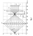
- Figure 6 shows a concentric to the central axis 35 of the change in emittance 21 and at a distance from the entrance plane 23 of the Device 21 arranged particle source 67 which is transverse to the Longitudinal axis 35 has an extent h.
- Figure 6 are further examples of a plurality of trajectories for electron orbits shown, namely two trajectories 69 and 69 ', which have such an angle with the longitudinal axis 35, that once a reflection through the electrode assemblies he follows.
- the emission change device 21 acts from the point of view of the viewer 75 such that this total radiation perceives what appears to come from a radiation source, which has an extent A transverse to the longitudinal axis 35 which in the example described in Figure 6, in which due to the limited beam divergence a maximum of two reflections at the Emittance changing device 21 occur five times Value of the extent h corresponds to the true source 67.
- the Divergence that is the angle to the longitudinal axis 35 or one Angular distribution of the at the outlet end 27 of the device 21 emerging rays is here through the device 21 compared to the entry of the rays at the entry end 23 not changed.
- the device since the apparent area of the Source is increased due to device 21, the device has 21 the light conductance or the emittance of the beam, which as the product of the square root of the illuminated Area and the lighting divergence is defined, increased.
- Figure 7 shows an embodiment of a lighting system 83, in which the emission change device 21 is integrated is.
- the longitudinal axis 35 of the emission change device 21 is aligned so that it with the optical Axis of the lighting system 83 coincides.
- Illumination system 83 is part of a lithography system, which further includes a projection system 84, which follows is explained in connection with Figure 8.
- An illuminated one Object 85 is a mask on which patterns are defined are, which with the projection system 84 on a radiation-sensitive layer 105 of a semiconductor wafer 107 can be projected.
- the radiation source 67 is one thermal electron source where the from the to about 2,000K heated cathode emitted through an electrode Voltage of 100 kV accelerated in the direction of the optical axis 35 become.
- the kinetic energy of the electrons in The direction of the axis 35 is therefore 100keV, while the kinetic Energy perpendicular to axis 35 maximum about 0.2 eV is.
- a maximum angle ⁇ that the trajectory of a maximum of electrons emitted from source 67 to optical ones Axis 35 occupies is thus about 1.4mrad.
- a focusing lens 87 produces 10 times in a plane 89 reduced image of source 67.
- Another focusing lens 91 is arranged on the optical axis so that it Image of source 67 in level 89 in an intermediate image level 93 depicts.
- the emittance changing device 21 is arranged, wherein this in the direction of the optical axis 35 has a length of 200 mm and has an edge length of about 10mm * 10mm across it.
- the intermediate image plane 93 is a third focusing lens 95 depicted on the mask 85 after infinity.
- Figure 7 are just a few examples of trajectories of electrons shown on their way from the source 67 to the mask 85.
- a group 97 of the trajectories shown in FIG. 7 is one of the electrons from source 67 under one are emitted so small angle ⁇ to the axis 35 that they pass through the emittance changing device 21 without reflection.
- the focusing lens produces 91 in for these electrons the intermediate level 93 an intermediate image 100 of the source 67, the is arranged on the longitudinal axis 35.
- These trajectories are parallelized by the focusing lens 95 so that they a very small one when it hits mask 85 Include angle ⁇ to axis 35.
- Another group 98 of trajectories belongs to such Electrons emitted by source 67 in such an area of the angle ⁇ to the axis 35 that they are in the Emission change device 21 can be reflected once.
- the focusing lens 91 generates Intermediate image plane 93 an intermediate image 101, which is at a distance is arranged by the optical axis 35.
- the focusing lens 95 also directs these electrons onto the mask 85, where they overlap with the electrons of bundle 97, there, however, at a much larger angle Hit ⁇ to axis 35.
- Another group 99 of trajectories belongs to the Electrons, which have an almost maximum emittance angle ⁇ of the source 67 are emitted. These electrons are in of the emittance changing device 21 reflected twice, and the focusing lens 91 forms an image for these electrons 102 of the image of source 67 in level 89. This after double reflection in the emittance changing device 21 resulting images 102 of the source 67 are from the optical Axis 35 arranged at an even greater distance than that Images 101 of the electrons that appear only once in the emittance changing device 21 were reflected.
- Images 102 are also transferred from the focusing lens 95 to the Mask 85 directed as a substantially parallel beam, with the electrons of bundles 97 and 98 overlap and with an even larger angle ⁇ to the axis 35 meet mask 85.
- the angle ⁇ to the longitudinal axis 35 for the latter group 99 of trajectories represent the maximum lighting aperture and is much larger than the maximum Divergence angle ⁇ of the source 67, although on the mask 85 square field with an edge length 1 of about 1mm is illuminated. In spite of its im Compared to the extent of the source 67 relatively large extent illuminated essentially homogeneously. From Figure 7 it can also be seen that the edge length 1 of the illuminated Field is less than the distance between the intermediate images 101 and 102 from the longitudinal axis 35.
- the projection system 84 shown in FIG. 8 forms the mask 85 on a radiation-sensitive layer 105, which on the side of a semiconductor wafer facing the mask 85 107 is applied.
- the projection system 84 includes a doublet of magnetic lenses 109 and 111, which on the Mask defines structures and patterns by a factor of 4 images reduced on the radiation-sensitive layer 105.
- three groups of trajectories are exemplary with a different distance M from the optical axis 35, with FIG. 8 also showing that the mask 85 through the lighting system shown in FIG 83 is illuminated with an illumination aperture ⁇ .
- the doublet of focusing lenses 109 and 111 guides the trajectories through a plane of symmetry 113, on which for the A crossover is formed, that is, the trajectories intersect the optical axis 35 there.
- a plane of symmetry 113 In this plane of symmetry 113 an aperture diaphragm 115 is also provided, which is penetrated by the rays that mask 85 have passed through without being scattered, while the electrons emitted by the mask 85 slightly scattered out of its original path are absorbed by the aperture 115 and so that it does not get onto the radiation-sensitive layer.
- Reference numerals 121, 123 and 125 denote in FIG. 8
- Auxiliary coils, which supplement the focusing lenses 109 and Provide 111 magnetic fields and which are controlled in this way can be that aberrations in the projection of the Mask 85 reduced to radiation-sensitive layer 105 become.
- the emission change device in a lighting system and a projection system used for the illustration serves a mask structure on a substrate.
- the emission change device 21 is the emission change device 21, however not limited. It can be used wherever for charged particles, an intervention on their trajectories should be made, the effect or change the trajectory from an angle of the trajectory an optical axis before entering the emittance changing device is dependent.
- the emittance changing device has been previously described such that they have an internal electrode arrangement and has an outer electrode arrangement, each of which have a square cross-section.
- the interior and External electrode arrangements circular cylindrical or any have other shapes.
- the arrangement of the cylindrical electrode arrangement was previously the emittance changing device as symmetrical represented to the incident beam. However, it is also possible between the incident beam and the cylinder's longitudinal axis to provide an angle or the cylinder longitudinal axis parallel to move to the incident beam.
- the sub-electrodes are of the emittance change device as tensioned Wires described.
Landscapes
- Chemical & Material Sciences (AREA)
- Engineering & Computer Science (AREA)
- Nanotechnology (AREA)
- Analytical Chemistry (AREA)
- Physics & Mathematics (AREA)
- Crystallography & Structural Chemistry (AREA)
- Manufacturing & Machinery (AREA)
- General Physics & Mathematics (AREA)
- Condensed Matter Physics & Semiconductors (AREA)
- Mathematical Physics (AREA)
- Theoretical Computer Science (AREA)
- Exposure And Positioning Against Photoresist Photosensitive Materials (AREA)
- Electron Beam Exposure (AREA)
Abstract
Description
- Figur 1
- eine Beleuchtungsvorrichtung, in deren Strahlengang eine erfindungsgemäße teilchenoptische Vorrichtung nicht angeordnet ist,
- Figur 2
- eine Ausführungsform einer erfindungsgemäßen teilchenoptischen Vorrichtung in schematisch perspektivischer Darstellung,
- Figur 3
- die teilchenoptische Vorrichtung gemäß Figur 1 in einer Schnittdarstellung,
- Figur 4
- eine Darstellung zur Funktion der in den Figuren 2 und 3 gezeigten Vorrichtung,
- Figur 5
- eine vergrößerte Darstellung eines in Figur 4 mit V gekennzeichneten Bereichs desselben,
- Figur 6
- eine weitere erläuternde Darstellung zur Funktion der in den Figuren 2 und 3 gezeigten Vorrichtung,
- Figur 7
- eine Ausführungsform eines erfindungsgemäßen Beleuchtungssystems und
- Figur 8
- eine Teilansicht einer Ausführungsform eines erfindungsgemäßen Projektionssystems.
Claims (13)
- Teilchenoptische Vorrichtung zum Ändern von Trajektorien (55, 98, 99) geladener Teilchen eines entlang einer Längsachse (35) orientierten divergenten Teilchenstrahls (25), umfassend:wobei die Spannungsquelle (47) eine solche Potentialdifferenz bereitstellt, daß eine quer zur Längsachse (35) orientierte Bewegungskomponenete eines die Innenelektrodenanordnung (37) durchsetzenden Teilchens umkehrbar ist.eine für die Teilchen wenigstens teilweise transparente Innenelektrodenanordnung (37), welche die Längsachse (35) mit radialem Abstand (D) wenigstens teilweise umgreift und sich entlang der Längsachse (35) erstreckt,eine Außenelektrodenanordnung (29), welche die Innenelektrodenanordnung (37) bezüglich der Längsachse (35) mit radialem Abstand (d) wenigstens teilweise umgreift und sich entlang der Längsachse (35) erstreckt, undeine Spannungsquelle (47) zum Bereitstellen einer Potentialdifferenz zwischen der Innenelektrodenanordnung (37) und der Außenelektrodenanordnung (29),
- Vorrichtung nach Anspruch 1, wobei die Innenelektrodenanordnung (37) eine Mehrzahl von mit Abstand in Umfangsrichtung um die Längsachse (35) voneinander angeordneten Teilelektroden (39) umfaßt.
- Vorrichtung nach Anspruch 2, wobei die Teilelektroden (39) sich im wesentlichen parallel zur Längsachse (35) erstrecken.
- Vorrichtung nach Anspruch 2 oder 3, wobei die Teilelektroden durch eine Mehrzahl Drähte (39) gebildet sind, die zwischen einem eintrittseitigen Halterahmen (43) und einem austrittseitigen Halterahmen (45) für die Drähte (39) eingespannt sind.
- Teilchenoptische Beleuchtungsvorrichtung zum Beleuchten eines in einer Objektebene angeordneten Objekts (85), umfassend:eine Teilchenquelle (67) zur Emission eines Strahls geladener Teilchen,eine zwischen der Teilchenquelle (67) und der Objektebene (85) angeordnete Emittanzänderungsvorrichtung (21), welche durch eine teilchenoptische Vorrichtung nach einem der Ansprüche 1 bis 4 gebildet ist und in welche von der Teilchenquelle (67) emittierte geladene Teilchen eintreten, undein Kondensorsystem, um von der Emittanzänderungsvorrichtung (21) austretende Teilchen auf die Objektebene (85) zu richten.
- Beleuchtungsvorrichtung nach Anspruch 5, wobei das Kondensorsystem eine erste Fokussierlinse (91) aufweist, welche die Quelle (67) oder ein in einer Quellbildebene (89) angeordnetes Bild der Quelle (67) in eine Zwischenebene (93) abbildet,
wobei die Emittanzänderungsvorrichtung (21) zwischen der Quelle (67) bzw. der Quellbildebene (89) und der ersten Fokussierlinse (91) angeordnet ist,
und wobei in der Zwischenebene (93) mehrere Bilder (101, 102) der Quelle (67) bzw. des Bildes der Quelle (67) erzeugt werden. - Beleuchtungsvorrichtung nach Anspruch 6, wobei das Kondensorsystem eine zweite Fokussierlinse (95) aufweist, um die mehreren Bilder (101, 102) der Quelle, bzw. des Bildes der Quelle, in der Objektebene (85) zu überlagern.
- Beleuchtungsvorrichtung nach Anspruch 7, wobei die Zwischenebene (93) eine Brennebene der zweiten Fokussierlinse (95) ist.
- Beleuchtungsvorrichtung nach einem der Ansprüche 5 bis 8, wobei zwischen der Quelle (67) und der Emittanzänderungsvorrichtung (21) wenigstens eine dritte Fokussierlinse (87) vorgesehen ist, um das von der ersten Fokussierlinse (91) in die Zwischenebene (93) abgebildete Bild der Quelle (67) zu erzeugen.
- Beleuchtungsvorrichtung nach Anspruch 5, wobei das Kondensorsystem eine erste Fokussierlinse (91) aufweist, welche die Teilchen, nach Durchlaufen der Emittanzänderungsvorrichtung, durch eine zwischen der Objektebene (85) und der ersten Fokussierlinse (91) angeordnete Zwischenebene (93) lenkt, und zwar derart, daß ein jedes Teilchen die Zwischenebene (93) mit einem Abstand von der Längsachse (35) durchsetzt, der um so größer ist, je öfter die orthogonal zur Längsachse (35) orientierte Bewegungskomponenete des Teilchens durch die Emittanzänderungsvorrichtung (21) geändert wurde.
- Beleuchtungsvorrichtung nach Anspruch 10, wobei das Kondensorsystem eine zweite Fokussierlinse (95) aufweist, um die Teilchen nach Durchlaufen der Zwischenebene (93) auf die Objektebene (85) zu richten, wobei ein maximaler Abstand von der Längsachse, mit dem die Teilchen auf die Objektebene (85) treffen, geringer ist als ein maximaler Abstand, mit dem die entsprechenden Teilchen die Zwischenebene (93) durchsetzen.
- Abbildungssystem zur Übertragung eines auf einer Maske (85) definierten Musters mittels eines Strahls geladener Teilchen auf ein in einer Substratebene anordenbares teilchenempfindliches Substrat (105), umfassend:wobei das Beleuchtungssystem (83) eine Beleuchtungsvorrichtung gemäß einem der Ansprüche 5 bis 11 umfaßt, in deren Objektebene die Maske (85) angeordnet ist.ein Beleuchtungssystem (83) zum Beleuchten der Maske (85) mit dem Strahl geladener Teilchen und eine teilchenoptische Abbildungsvorrichtung (84) zum Abbilden der Maske (85) auf das Substrat (105),
- Verfahren zur Herstellung eines Bauelements, umfassend wenigstens einen photolithographischen Schritt, wobei der photolithographische Schritt umfaßt:Bereitstellen des Abbildungsystems nach Anspruch 12,Anordnen eines mit einer teilchenempfindlichen Schicht versehenen Substrats in der Substratebene, undBelichten des teilchenempfindlichen Substrats mittels des Projektionssystems, wobei ein durch die Maske bereitgestelltes Muster auf die teilchenempfindliche Schicht übertragen wird.
Applications Claiming Priority (2)
| Application Number | Priority Date | Filing Date | Title |
|---|---|---|---|
| DE10117025A DE10117025A1 (de) | 2001-04-05 | 2001-04-05 | Teilchenoptische Vorrichtung,Beleuchtungsvorrichtung und Projektionssystem sowie Verfahren unter Verwendung derselben |
| DE10117025 | 2001-04-05 |
Publications (2)
| Publication Number | Publication Date |
|---|---|
| EP1248282A1 true EP1248282A1 (de) | 2002-10-09 |
| EP1248282B1 EP1248282B1 (de) | 2007-11-28 |
Family
ID=7680525
Family Applications (1)
| Application Number | Title | Priority Date | Filing Date |
|---|---|---|---|
| EP02007523A Expired - Lifetime EP1248282B1 (de) | 2001-04-05 | 2002-04-02 | Teilchenoptische Vorrichtung, Beleuchtungsvorrichtung und Projektionssystem sowie Verfahren unter Verwendung derselben |
Country Status (6)
| Country | Link |
|---|---|
| US (1) | US6756599B2 (de) |
| EP (1) | EP1248282B1 (de) |
| JP (1) | JP4053333B2 (de) |
| CZ (1) | CZ300612B6 (de) |
| DE (2) | DE10117025A1 (de) |
| TW (1) | TW578189B (de) |
Families Citing this family (4)
| Publication number | Priority date | Publication date | Assignee | Title |
|---|---|---|---|---|
| US7405402B1 (en) * | 2006-02-21 | 2008-07-29 | Kla-Tencor Technologies Corporation | Method and apparatus for aberration-insensitive electron beam imaging |
| US9184040B2 (en) * | 2011-06-03 | 2015-11-10 | Bruker Daltonics, Inc. | Abridged multipole structure for the transport and selection of ions in a vacuum system |
| US8927940B2 (en) * | 2011-06-03 | 2015-01-06 | Bruker Daltonics, Inc. | Abridged multipole structure for the transport, selection and trapping of ions in a vacuum system |
| US8969798B2 (en) * | 2011-07-07 | 2015-03-03 | Bruker Daltonics, Inc. | Abridged ion trap-time of flight mass spectrometer |
Citations (2)
| Publication number | Priority date | Publication date | Assignee | Title |
|---|---|---|---|---|
| US5633507A (en) * | 1995-09-19 | 1997-05-27 | International Business Machines Corporation | Electron beam lithography system with low brightness |
| US6069684A (en) * | 1998-02-04 | 2000-05-30 | International Business Machines Corporation | Electron beam projection lithography system (EBPS) |
Family Cites Families (26)
| Publication number | Priority date | Publication date | Assignee | Title |
|---|---|---|---|---|
| US3735128A (en) * | 1971-08-27 | 1973-05-22 | Physical Electronics Ind Inc | Field termination plate |
| US4376249A (en) * | 1980-11-06 | 1983-03-08 | International Business Machines Corporation | Variable axis electron beam projection system |
| DE3138898A1 (de) * | 1981-09-30 | 1983-04-14 | Siemens AG, 1000 Berlin und 8000 München | Elektrostatisches ablenksystem |
| US4556823A (en) * | 1983-07-28 | 1985-12-03 | International Business Machines Corporation | Multi-function charged particle apparatus |
| US5079112A (en) | 1989-08-07 | 1992-01-07 | At&T Bell Laboratories | Device manufacture involving lithographic processing |
| US5258246A (en) | 1989-08-07 | 1993-11-02 | At&T Bell Laboratories | Device manufacture involving lithographic processing |
| US5130213A (en) | 1989-08-07 | 1992-07-14 | At&T Bell Laboratories | Device manufacture involving lithographic processing |
| US5260151A (en) | 1991-12-30 | 1993-11-09 | At&T Bell Laboratories | Device manufacture involving step-and-scan delineation |
| US5376505A (en) | 1992-03-16 | 1994-12-27 | At&T Corp. | Device fabrication entailing submicron imaging |
| RU2002981C1 (ru) * | 1992-03-27 | 1993-11-15 | Индивидуальное частное предпри тие Анисимовой "АЛС" | Способ формировани закрученных потоков |
| US5316879A (en) | 1992-07-14 | 1994-05-31 | At&T Bell Laboratories | Sub-micron device fabrication using multiple aperture filter |
| US6285443B1 (en) | 1993-12-13 | 2001-09-04 | Carl-Zeiss-Stiftung | Illuminating arrangement for a projection microlithographic apparatus |
| EP0658810B1 (de) | 1993-12-13 | 1998-11-25 | Carl Zeiss | Beleuchtungseinrichtung für ein optisches System mit einem Reticle-Maskierungssystem |
| DE19520563A1 (de) | 1995-06-06 | 1996-12-12 | Zeiss Carl Fa | Beleuchtungseinrichtung für ein Projektions-Mikrolithographie-Gerät |
| US5805620A (en) | 1994-04-08 | 1998-09-08 | Southeastern Universities Research Association | Beam conditioner for free electron lasers and synchrotrons |
| US5912469A (en) * | 1996-07-11 | 1999-06-15 | Nikon Corporation | Charged-particle-beam microlithography apparatus |
| JPH10112274A (ja) | 1996-08-12 | 1998-04-28 | Nikon Corp | 電子銃 |
| JP3323412B2 (ja) | 1996-12-05 | 2002-09-09 | 理化学研究所 | 荷電粒子ビームの輸送システム |
| DE19738070A1 (de) | 1997-09-01 | 1999-03-04 | Leo Elektronenmikroskopie Gmbh | Energiefilter, insbesondere für ein Elektronenmikroskop |
| DE19855629A1 (de) | 1998-12-02 | 2000-06-08 | Leo Elektronenmikroskopie Gmbh | Teilchenoptische Anordnung und Verfahren zur teilchenoptischen Erzeugung von Mikrostrukturen |
| US6014200A (en) | 1998-02-24 | 2000-01-11 | Nikon Corporation | High throughput electron beam lithography system |
| US6091187A (en) | 1998-04-08 | 2000-07-18 | International Business Machines Corporation | High emittance electron source having high illumination uniformity |
| US6051346A (en) * | 1998-04-29 | 2000-04-18 | Lucent Technologies Inc. | Process for fabricating a lithographic mask |
| EP0969326B1 (de) | 1998-07-01 | 2012-10-17 | ASML Netherlands B.V. | Lithographischer Apparat |
| DE19946447B4 (de) * | 1998-10-13 | 2012-01-19 | Ims Nanofabrication Ag | Teilchenoptisches Abbildungssystem für Lithographiezwecke |
| DE19855106A1 (de) | 1998-11-30 | 2000-05-31 | Zeiss Carl Fa | Beleuchtungssystem für die VUV-Mikrolithographie |
-
2001
- 2001-04-05 DE DE10117025A patent/DE10117025A1/de not_active Withdrawn
-
2002
- 2002-03-27 TW TW091106070A patent/TW578189B/zh not_active IP Right Cessation
- 2002-04-02 DE DE50211269T patent/DE50211269D1/de not_active Expired - Lifetime
- 2002-04-02 EP EP02007523A patent/EP1248282B1/de not_active Expired - Lifetime
- 2002-04-03 JP JP2002100798A patent/JP4053333B2/ja not_active Expired - Lifetime
- 2002-04-04 US US10/115,886 patent/US6756599B2/en not_active Expired - Lifetime
- 2002-04-04 CZ CZ20021178A patent/CZ300612B6/cs not_active IP Right Cessation
Patent Citations (2)
| Publication number | Priority date | Publication date | Assignee | Title |
|---|---|---|---|---|
| US5633507A (en) * | 1995-09-19 | 1997-05-27 | International Business Machines Corporation | Electron beam lithography system with low brightness |
| US6069684A (en) * | 1998-02-04 | 2000-05-30 | International Business Machines Corporation | Electron beam projection lithography system (EBPS) |
Non-Patent Citations (1)
| Title |
|---|
| D.MOONEN ET AL: "Grid lens approach for high effective emittance in SCALPEL", J.VAC. SCI. TECHNOL. B, vol. 18, no. 6, - 2000, pages 3111 - 3114, XP002203648 * |
Also Published As
| Publication number | Publication date |
|---|---|
| DE10117025A1 (de) | 2002-10-10 |
| DE50211269D1 (de) | 2008-01-10 |
| US6756599B2 (en) | 2004-06-29 |
| JP4053333B2 (ja) | 2008-02-27 |
| EP1248282B1 (de) | 2007-11-28 |
| CZ300612B6 (cs) | 2009-07-01 |
| US20020179845A1 (en) | 2002-12-05 |
| JP2005038606A (ja) | 2005-02-10 |
| TW578189B (en) | 2004-03-01 |
| CZ20021178A3 (cs) | 2002-11-13 |
Similar Documents
| Publication | Publication Date | Title |
|---|---|---|
| DE69817787T2 (de) | Rasterelektronenmikroskop mit elektrostatischem objektiv und elektrische abtastvorrichtung | |
| DE19848070B4 (de) | Niedrigenergie-Elektronenstrahllithographie | |
| EP1280184B1 (de) | Untersuchungssystem zum teilchenoptischen Abbilden eines Objekts, Ablenkvorrichtung für geladene Teilchen sowie Verfahren zum Betrieb derselben | |
| DE102008035297B4 (de) | Aberrationskorrektureinrichtung für Ladungsteilchenstrahlen in einem optischen System einer Ladungsteilchenstrahlvorrichtung und Ladungsteilchenstrahlvorrichtung mit der Aberrationskorrektureinrichtung | |
| DE69233067T2 (de) | Integrierte Schaltungen | |
| DE69027602T2 (de) | Energiefilter für Ladungsträgervorrichtung | |
| EP0180723B1 (de) | Korpuskularstrahlgerät | |
| EP0075712B1 (de) | Elektronenoptisches System zur Erzeugung eines Elektronen-Formstrahl mit variablem Strahlquerschnitt, insbesondere zur Erzeugung von Mikrostrukturen | |
| EP1389794B1 (de) | Strahlführungssystem, Abbildungsverfahren und Elektronenmikroskopiesystem | |
| DE3933317A1 (de) | Saeule zur erzeugung eines fokussierten ionenstrahls | |
| EP0106154B1 (de) | Varioformstrahl-Ablenkobjektiv für Neutralteilchen und Verfahren zu seinem Betrieb | |
| DE19946447B4 (de) | Teilchenoptisches Abbildungssystem für Lithographiezwecke | |
| EP1239510B1 (de) | Teilchenoptische Linsenanordnung und Verfahren unter Einsatz einer solchen Linsenanordnung | |
| EP0739531B1 (de) | Teilchenoptisches abbildungssystem | |
| DE10232689A1 (de) | Mit Strahlen geladener Teilchen arbeitende Anwendungen | |
| EP0564438A1 (de) | Teilchen-, insbes. ionenoptisches Abbildungssystem | |
| DE69605053T2 (de) | Kanonenlinse zur Partikelstrahlerzeugung | |
| DE3919829C2 (de) | Elektronenkanonen-System mit Feldemission | |
| EP0523033A1 (de) | Ionenoptisches Abbildungssystem | |
| DE19734059B4 (de) | Anordnung für Schattenwurflithographie | |
| DE29915847U1 (de) | Steuerung der Beleuchtungsverteilung in der Austrittspupille eines EUV-Beleuchtungssystems | |
| EP1248282B1 (de) | Teilchenoptische Vorrichtung, Beleuchtungsvorrichtung und Projektionssystem sowie Verfahren unter Verwendung derselben | |
| DE102016120902B4 (de) | Vielstrahl-Teilchenmikroskop | |
| DE10237135A1 (de) | Teilchenoptische Vorrichtung und Verfahren zum Betrieb derselben | |
| DE69913313T2 (de) | Quadrupol-Vorrichtung für Projektionslithographie mittels geladener Teilchen |
Legal Events
| Date | Code | Title | Description |
|---|---|---|---|
| PUAI | Public reference made under article 153(3) epc to a published international application that has entered the european phase |
Free format text: ORIGINAL CODE: 0009012 |
|
| AK | Designated contracting states |
Kind code of ref document: A1 Designated state(s): AT BE CH CY DE DK ES FI FR GB GR IE IT LI LU MC NL PT SE TR |
|
| AX | Request for extension of the european patent |
Free format text: AL;LT;LV;MK;RO;SI |
|
| 17P | Request for examination filed |
Effective date: 20021125 |
|
| RAP1 | Party data changed (applicant data changed or rights of an application transferred) |
Owner name: CARL ZEISS SMT AG |
|
| AKX | Designation fees paid |
Designated state(s): DE FR GB IT NL |
|
| 17Q | First examination report despatched |
Effective date: 20050322 |
|
| GRAP | Despatch of communication of intention to grant a patent |
Free format text: ORIGINAL CODE: EPIDOSNIGR1 |
|
| GRAC | Information related to communication of intention to grant a patent modified |
Free format text: ORIGINAL CODE: EPIDOSCIGR1 |
|
| RAP1 | Party data changed (applicant data changed or rights of an application transferred) |
Owner name: CARL ZEISS SMT AG |
|
| GRAS | Grant fee paid |
Free format text: ORIGINAL CODE: EPIDOSNIGR3 |
|
| GRAA | (expected) grant |
Free format text: ORIGINAL CODE: 0009210 |
|
| AK | Designated contracting states |
Kind code of ref document: B1 Designated state(s): DE FR GB IT NL |
|
| REF | Corresponds to: |
Ref document number: 50211269 Country of ref document: DE Date of ref document: 20080110 Kind code of ref document: P |
|
| GBT | Gb: translation of ep patent filed (gb section 77(6)(a)/1977) |
Effective date: 20080116 |
|
| EN | Fr: translation not filed | ||
| PLBE | No opposition filed within time limit |
Free format text: ORIGINAL CODE: 0009261 |
|
| STAA | Information on the status of an ep patent application or granted ep patent |
Free format text: STATUS: NO OPPOSITION FILED WITHIN TIME LIMIT |
|
| PG25 | Lapsed in a contracting state [announced via postgrant information from national office to epo] |
Ref country code: FR Free format text: LAPSE BECAUSE OF FAILURE TO SUBMIT A TRANSLATION OF THE DESCRIPTION OR TO PAY THE FEE WITHIN THE PRESCRIBED TIME-LIMIT Effective date: 20080912 |
|
| 26N | No opposition filed |
Effective date: 20080829 |
|
| PGFP | Annual fee paid to national office [announced via postgrant information from national office to epo] |
Ref country code: FR Payment date: 20080412 Year of fee payment: 7 |
|
| PGFP | Annual fee paid to national office [announced via postgrant information from national office to epo] |
Ref country code: NL Payment date: 20100413 Year of fee payment: 9 |
|
| PGFP | Annual fee paid to national office [announced via postgrant information from national office to epo] |
Ref country code: GB Payment date: 20100420 Year of fee payment: 9 |
|
| PG25 | Lapsed in a contracting state [announced via postgrant information from national office to epo] |
Ref country code: IT Free format text: LAPSE BECAUSE OF NON-PAYMENT OF DUE FEES Effective date: 20080430 |
|
| REG | Reference to a national code |
Ref country code: NL Ref legal event code: V1 Effective date: 20111101 |
|
| GBPC | Gb: european patent ceased through non-payment of renewal fee |
Effective date: 20110402 |
|
| PG25 | Lapsed in a contracting state [announced via postgrant information from national office to epo] |
Ref country code: NL Free format text: LAPSE BECAUSE OF NON-PAYMENT OF DUE FEES Effective date: 20111101 |
|
| PG25 | Lapsed in a contracting state [announced via postgrant information from national office to epo] |
Ref country code: GB Free format text: LAPSE BECAUSE OF NON-PAYMENT OF DUE FEES Effective date: 20110402 |
|
| PGFP | Annual fee paid to national office [announced via postgrant information from national office to epo] |
Ref country code: DE Payment date: 20210420 Year of fee payment: 20 |
|
| REG | Reference to a national code |
Ref country code: DE Ref legal event code: R071 Ref document number: 50211269 Country of ref document: DE |