EP1246325A2 - Laser working dielectric substrate and method for working same and semiconductor package and method for manufacturing same - Google Patents
Laser working dielectric substrate and method for working same and semiconductor package and method for manufacturing same Download PDFInfo
- Publication number
- EP1246325A2 EP1246325A2 EP02006503A EP02006503A EP1246325A2 EP 1246325 A2 EP1246325 A2 EP 1246325A2 EP 02006503 A EP02006503 A EP 02006503A EP 02006503 A EP02006503 A EP 02006503A EP 1246325 A2 EP1246325 A2 EP 1246325A2
- Authority
- EP
- European Patent Office
- Prior art keywords
- substrate
- laser
- dielectric substrate
- semiconductor package
- working
- Prior art date
- Legal status (The legal status is an assumption and is not a legal conclusion. Google has not performed a legal analysis and makes no representation as to the accuracy of the status listed.)
- Withdrawn
Links
Images







Classifications
-
- H—ELECTRICITY
- H01—ELECTRIC ELEMENTS
- H01S—DEVICES USING THE PROCESS OF LIGHT AMPLIFICATION BY STIMULATED EMISSION OF RADIATION [LASER] TO AMPLIFY OR GENERATE LIGHT; DEVICES USING STIMULATED EMISSION OF ELECTROMAGNETIC RADIATION IN WAVE RANGES OTHER THAN OPTICAL
- H01S5/00—Semiconductor lasers
- H01S5/02—Structural details or components not essential to laser action
-
- H—ELECTRICITY
- H05—ELECTRIC TECHNIQUES NOT OTHERWISE PROVIDED FOR
- H05K—PRINTED CIRCUITS; CASINGS OR CONSTRUCTIONAL DETAILS OF ELECTRIC APPARATUS; MANUFACTURE OF ASSEMBLAGES OF ELECTRICAL COMPONENTS
- H05K3/00—Apparatus or processes for manufacturing printed circuits
- H05K3/0011—Working of insulating substrates or insulating layers
- H05K3/0017—Etching of the substrate by chemical or physical means
- H05K3/0026—Etching of the substrate by chemical or physical means by laser ablation
- H05K3/0032—Etching of the substrate by chemical or physical means by laser ablation of organic insulating material
-
- H—ELECTRICITY
- H05—ELECTRIC TECHNIQUES NOT OTHERWISE PROVIDED FOR
- H05K—PRINTED CIRCUITS; CASINGS OR CONSTRUCTIONAL DETAILS OF ELECTRIC APPARATUS; MANUFACTURE OF ASSEMBLAGES OF ELECTRICAL COMPONENTS
- H05K1/00—Printed circuits
- H05K1/02—Details
- H05K1/03—Use of materials for the substrate
- H05K1/0313—Organic insulating material
- H05K1/0353—Organic insulating material consisting of two or more materials, e.g. two or more polymers, polymer + filler, + reinforcement
- H05K1/0366—Organic insulating material consisting of two or more materials, e.g. two or more polymers, polymer + filler, + reinforcement reinforced, e.g. by fibres, fabrics
-
- H—ELECTRICITY
- H05—ELECTRIC TECHNIQUES NOT OTHERWISE PROVIDED FOR
- H05K—PRINTED CIRCUITS; CASINGS OR CONSTRUCTIONAL DETAILS OF ELECTRIC APPARATUS; MANUFACTURE OF ASSEMBLAGES OF ELECTRICAL COMPONENTS
- H05K1/00—Printed circuits
- H05K1/02—Details
- H05K1/03—Use of materials for the substrate
- H05K1/0313—Organic insulating material
- H05K1/0353—Organic insulating material consisting of two or more materials, e.g. two or more polymers, polymer + filler, + reinforcement
- H05K1/0373—Organic insulating material consisting of two or more materials, e.g. two or more polymers, polymer + filler, + reinforcement containing additives, e.g. fillers
-
- H—ELECTRICITY
- H05—ELECTRIC TECHNIQUES NOT OTHERWISE PROVIDED FOR
- H05K—PRINTED CIRCUITS; CASINGS OR CONSTRUCTIONAL DETAILS OF ELECTRIC APPARATUS; MANUFACTURE OF ASSEMBLAGES OF ELECTRICAL COMPONENTS
- H05K2201/00—Indexing scheme relating to printed circuits covered by H05K1/00
- H05K2201/01—Dielectrics
- H05K2201/0104—Properties and characteristics in general
- H05K2201/0112—Absorbing light, e.g. dielectric layer with carbon filler for laser processing
-
- H—ELECTRICITY
- H05—ELECTRIC TECHNIQUES NOT OTHERWISE PROVIDED FOR
- H05K—PRINTED CIRCUITS; CASINGS OR CONSTRUCTIONAL DETAILS OF ELECTRIC APPARATUS; MANUFACTURE OF ASSEMBLAGES OF ELECTRICAL COMPONENTS
- H05K2201/00—Indexing scheme relating to printed circuits covered by H05K1/00
- H05K2201/02—Fillers; Particles; Fibers; Reinforcement materials
- H05K2201/0203—Fillers and particles
- H05K2201/0206—Materials
- H05K2201/0209—Inorganic, non-metallic particles
-
- H—ELECTRICITY
- H10—SEMICONDUCTOR DEVICES; ELECTRIC SOLID-STATE DEVICES NOT OTHERWISE PROVIDED FOR
- H10W—GENERIC PACKAGES, INTERCONNECTIONS, CONNECTORS OR OTHER CONSTRUCTIONAL DETAILS OF DEVICES COVERED BY CLASS H10
- H10W72/00—Interconnections or connectors in packages
- H10W72/851—Dispositions of multiple connectors or interconnections
- H10W72/874—On different surfaces
- H10W72/884—Die-attach connectors and bond wires
-
- H—ELECTRICITY
- H10—SEMICONDUCTOR DEVICES; ELECTRIC SOLID-STATE DEVICES NOT OTHERWISE PROVIDED FOR
- H10W—GENERIC PACKAGES, INTERCONNECTIONS, CONNECTORS OR OTHER CONSTRUCTIONAL DETAILS OF DEVICES COVERED BY CLASS H10
- H10W90/00—Package configurations
- H10W90/701—Package configurations characterised by the relative positions of pads or connectors relative to package parts
- H10W90/731—Package configurations characterised by the relative positions of pads or connectors relative to package parts of die-attach connectors
- H10W90/734—Package configurations characterised by the relative positions of pads or connectors relative to package parts of die-attach connectors between a chip and a stacked insulating package substrate, interposer or RDL
-
- H—ELECTRICITY
- H10—SEMICONDUCTOR DEVICES; ELECTRIC SOLID-STATE DEVICES NOT OTHERWISE PROVIDED FOR
- H10W—GENERIC PACKAGES, INTERCONNECTIONS, CONNECTORS OR OTHER CONSTRUCTIONAL DETAILS OF DEVICES COVERED BY CLASS H10
- H10W90/00—Package configurations
- H10W90/701—Package configurations characterised by the relative positions of pads or connectors relative to package parts
- H10W90/751—Package configurations characterised by the relative positions of pads or connectors relative to package parts of bond wires
- H10W90/754—Package configurations characterised by the relative positions of pads or connectors relative to package parts of bond wires between a chip and a stacked insulating package substrate, interposer or RDL
Definitions
- the present invention relates to a dielectric substrate suited as a high-frequency circuit substrate requiring low dielectric loss and method for working same and to a semiconductor package utilizing it and method for manufacturing same and, more particularly, to a dielectric substrate for use in a circuit on a high-frequency band including a micro-or-millimeter wave and method for working same and to a semiconductor package and method for manufacturing same.
- the substrate for use in a high-frequency circuit on a micro-or-millimeter wave, is desirably formed of a material having, as a material characteristic of a substrate, a low dielectric loss in order to suppress the dielectric loss due to the substrate per se in the circuit.
- Fig. 1 is an explanatory view showing an effect of dielectric loss a high-frequency circuit substrate itself possesses in its nature upon a signal flowing through a transmission line.
- the electric line of force 104 passes an interior of a substrate 101 to reach a ground electrode 103.
- the electric line of force 104 undergoes an affection of the dielectric loss the substrate 101 inherently possesses (given in a value of dielectric tangent).
- the loss in this case turns into heat energy, causing a phenomenon to generate heat upon the substrate 101. Consequently, the substrate for use in the high-frequency circuit is selected to have a characteristic low in dielectric coefficient and dielectric loss.
- the general organic material e.g. glass-epoxy
- the dielectric constant conspicuously worsens at a micro or millimeter wave band of 1 GH 2 or longer, due to the relationship between potential polarization in the material and frequency response. For this reason, there are less cases of the use as a substrate for high-frequency (approx. 1 GHz or higher) applications.
- an inorganic material such as alumina (dielectric constant: approx. 9, dielectric tangent: approx. 0.001), zirconia (dielectric constant: approx. 8, dielectric tangent: approx. 0.001) and aluminum nitride (dielectric constant: approx. 8, dielectric tangent: approx. 0.001).
- glass such as quartz is low in dielectric constant (dielectric constant: approx. 4) and dielectric loss (dielectric tangent: 0.001 or less), and hopeful as a material of a high-frequency circuit substrate.
- dielectric constant dielectric constant: approx. 4
- dielectric loss dielectric tangent: 0.001 or less
- glass conventionally there have been less cases to use glass for a high-frequency circuit substrate because of difficulty in partly working a through-holes or the like required in a circuit substrate.
- the high-frequency circuit on a micro and millimeter wave band in a communication system to radiocommunicate a great deal of information including moving pictures, has an extremely high frequency band.
- thermal loss is not negligible.
- glass such as quartz having a further low dielectric constant and loss.
- the means for forming a penetration hole through the glass substrate includes ultrasonic working, etch working, sandblast working and laser working.
- ultrasonic working however, the tool is to be worn during working and limited in its size despite the capability of realizing the formation of a multiplicity of holes at one time.
- glass In etch working, glass is materially stable and to be etched with a solution of hydrogen fluoride, phosphoric acid or alkali. However, the etch rate is extremely low, i.e. approximately 1 ⁇ m/h.
- Sandblast working generally allows for working of maximally about two times a mask thickness in a depth direction. Accordingly, ultrasonic working, etching working and sandblast working, in any, are not suited as a method to form penetration holes through a glass substrate.
- laser working is used in a massproducing process to form penetration holes or the like in an alumina substrate, and is free from substrate-size restriction. Accordingly, it is a working method suited for general substrate working.
- laser working when applied on glass substrates includes the following problems.
- the glass substrate can be worked as demonstrated, e.g. in the magazine "Materials Integration Vol.13 No.3 (2000)" pp.67-73.
- a ultra-short pulse laser system is expensive and high in running cost, hence being difficult in application to a mass-production process.
- YAG laser (wavelength: 1.06 ⁇ m) can work a finer shape than CO 2 laser working, in working a glass-epoxy substrate or the like due to the recent requirement for microfabrication. In place of CO 2 laser working, this has being placed into practical use. Because of lower in price and running cost than the other laser working systems, the working means is suited for mass production. However, because YAG laser has a wavelength (1.06 ⁇ m) to transmit through glass, it is not absorbed in glass and difficult in application to glass working. If energy density is raised in order to cause multiphoton absorption, cracks take place in the glass thus making impossible to obtain favorable worked form.
- the present invention has been made in view of the foregoing points, which provides a dielectric substrate and method for working same capable of coping with mass-production processing, in working a dielectric substrate such as a glass substrate and a resin substrate by the use of a laser. More particularly, it is an object to provide a dielectric substrate which is to be worked by using a YAG laser low in price and running cost, and a method for working same.
- the invention has a dielectric substrate for laser working containing a substance having to of a laser light wavelength and different in refractive index from a material of the dielectric substrate, thereby improving the efficiency and form in laser working a dielectric substrate.
- the invention has a quartz substrate containing therein bubbles, thereby further improving a high-frequency material characteristic of the substrate itself and improving the workability in forming a throughhole owing to bubble containment.
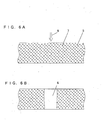
- Fig. 2 shows a sectional view of a glass substrate in a laser-working wherein a glass substrate 1 of quartz or the like contains bubbles 2.
- Fig. 2A represents a state prior to the laser working while Fig. 2B a state after laser working.
- the bubbles 2 are usually contained in such a manner that the bubbles 2 are scattered at random in the glass substrate 1.
- a penetration hole 3 is formed in the glass substrate 1 by laser working.
- the penetration hole 3 is nearly linearly formed extending along an irradiation direction of the laser beam 8, having a conspicuously improved form.
- the reason why laser workability on the glass substrate 1 containing bubbles 2 is improved is due to the following.
- quartz is superior in high frequency characteristic to alumina generally used as .a dielectric substrate material for high-frequency applications.
- the high frequency characteristic can be further improved by the containment of bubbles. This is because air in the bubble is an ideal dielectric which has a dielectric constant of 1 and a dielectric loss of 0.
- the apparent dielectric constant and loss of the material is made to a lower value than that of quartz in a singular form.
- Table 1 shows an example of the working conditions under which various laser have been used to form a penetration hole through a 1-mm-thick quartz glass spotted with bubbles of 1- 90 ⁇ m.
- Working Conditions of Bubble-contained Quartz Glass by Various Lasers Laser scheme Wavelength output form of Laser Power Shots RF excited CO 2 laser 10.6 ⁇ m Pulse (pulse width: 10msec) 200W 1 shot YAG laser 1.06 ⁇ m Pulse (pulse width: 500 ⁇ sec.) 1.1J 5 shots Semiconductor diode laser 0.81 ⁇ m Continuous 470W 3 seconds
- a penetration hole can be formed in the bubble-containing quartz glass by an RF excited CO 2 laser, a YAG laser or a semiconductor diode laser.
- the reason why the bubble-containing quartz glass can be worked at a low energy as shown in Table 1 is due to the following. Namely, a laser beam at low energy first causes fine cracks in the bubble-containing quartz glass and then the cracks successively propagate through fine bubbles, thereby accelerating the working. Incidentally, the working surface is extremely smooth because of laser irradiation and, at the same time, almost free of deterioration due to heat at or around the penetration hole to be caused in usually working quartz glass by a CO 2 laser. This can be considered because the bubbles in quartz glass provide an adiabatic effect to prevent the generated heat from spreading.
- the usual quartz glass cannot be worked by a YAG laser whereas the bubble-containing quartz glass can be worked by a YAG laser.
- the usual quartz glass has an optical characteristic that, at a YAG laser wavelength of 1.06 ⁇ m, energy absorption does not occur but the major part of energy transmits.
- the absorption-wavelength characteristic of the usual quartz glass can be changed to enable working.
- Embodiment 1 Although effective in working with a CO 2 laser, has a somewhat problem when worked by a YAG laser more inexpensive than a CO 2 laser. This is because the YAG laser is lower in output energy than the CO 2 laser. For this reason, this embodiment is set with the following conditions for the bubbles to be mixed in quartz glass.
- Table 2 shows the working conditions on bubblecontaining glass substrate by a YAG laser.
- Working Conditions on Bubble-containing Glass by a YAG Laser Bubble size Volume content ratio of bubbles YAG laser workability Corresponding figure Sample A 0.1 ⁇ 0.5 ⁇ m Approx. 10% Only crater formed Fig. 4 Sample B 2.0 ⁇ 5.0 ⁇ m Approx. 5% Penetration hole formed Fig. 3 Sample C 100 ⁇ 200 ⁇ m Approx. 12% Not formed ----
- Example A has a bubble size of 0.1 ⁇ m - 0.5 ⁇ m and a volume content ratio of bubbles of approximately 10%
- Sample B has a bubble size of 2.0 ⁇ m - 5.0 ⁇ m and a volume content ratio of bubbles of approximately 5%
- Sample C has a bubble size of 100 ⁇ m - 200 ⁇ m and a volume content ratio of bubbles of approximately 12%.
- a penetration hole having a diameter of 100 ⁇ m could be opened by one pulse of a laser having a pulse width of 0.5 msec and a power of 0.8J. Meanwhile, with a longer pulse width or higher power than that condition, a penetration hole could be opened.
- the quartz glass in this case has a section as shown in Figs. 2A and 2B.
- Fig. 2A is a state prior to laser working while Fig. 2B a state after laser working.
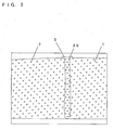
- Fig. 3 is a detailed view of a penetration hole worked by a YAG laser on the Sample B, which is an illustrative view of a section of a scanning electronic microscope picture of a penetration hole formed by one pulse of a YAG laser having a pulse width of 0.8 msec. and a power of 1.0J.
- a penetration hole 3 is formed nearly in a straight line form extending along a direction of laser light irradiation. Bubbles 20 in a semi-fused state are formed in an inner wall of the penetration hole 3.
- Fig. 4 is an example of laser working on Sample A, which is a scanning electronic microscopic picture as observed a laser working state from above. This shows a state that a crater 4 is formed in an upper surface of the glass substrate 1.
- Sample A and Sample B contain bubbles in a size of from one-tenth to ten times a laser light wavelength. It is to be presumed that the working by the YAG laser on these samples be made by the occurrence of laser beam 8 absorption owing to the size of bubbles. On the other hand, it can be considered that, on Sample C, the bubbles 2 be too large to cause absorption of the laser beam 8 when worked by a YAG laser.
- the bubbles 20 in a semi-fused state are observed in an innerwall surface of the penetration hole 3 as can be seen in Fig. 3. It can be presumed that all the bubbles 2 will not vanish in the YAG laser working with a result that hole working is favorably made. Accordingly, it can be seen that, in YAG laser working, the size of the bubbles 2 existing in the glass substrate 1 dominates workability.
- the bubble size in Sample B is 2.0 - 5.0 ⁇ m.
- the volume content ratio of bubbles 2 in the glass substrate 1 is desirably 5% or higher from the fact that, in the working of Sample B, YAG laser working on the glass substrate 1 was confirmed at a content ratio of bubbles 2 of approximately 5%. It can be presumed that laser working is easier as the content ratio of bubble 2 increases. However, in the case the content ratio of bubbles 2 is excessively high, the glass substrate 1 itself is ready to be broken. Consequently, the bubble content is practically limited generally to approximately 50%.
- the volume content ratio of bubbles 2 is practically in a range of 5 - 50%.
- the present embodiment can work a quartz glass substrate generally having difficulty in working by the use of an inexpensive YAG laser, enabling quartz substrate working excellent in mass producibility. Consequently, it is possible to inexpensively obtain a dielectric substrate extremely low in dielectric constant and loss preferable for a high-frequency circuit substrate for micro-or-millimeter wave applications. Thus, the use of the dielectric substrate provides a high-frequency circuit extremely low in heat loss.
- the quartz glass substrate containing bubbles in the embodiment can be favorably worked at low cost similarly to that with a YAG laser, by the use of an excimer laser, such as an ArF laser, a KrF laser or an F 2 laser, instead of a YAG laser.
- an excimer laser such as an ArF laser, a KrF laser or an F 2 laser
- the dielectric substrate working using a laser of the invention can realize the working to cause the similar effect on a dielectric substrate mixed with fine particles in a resin substrate, besides the working on the quartz glass substrate as described in Embodiments 1 and 2.
- the resins such as polyimide, liquid-crystal polymer, benzocyclobutene and PPE (polyphenyle ether), are known as dielectric materials having low dielectric constant and loss.
- the penetration hole 6 formed in a resin substrate 5 will be uneven in shape as shown in Fig. 5.
- the workability with a YAG laser can be improved by containing fine particles in the resin substrate 5.
- Fig. 6 shows a typical view that fine particles are contained in a resin substrate to improve YAG laser workability.
- Fig. 6A is a sectional view in a state prior to laser working while
- Fig. 6B is a sectional view in a state of after laser working.
- a fine glass bead 7 is contained as fine particles in a resin substrate 5.
- a penetration hole 6 is formed nearly in a straight-line form extending along a direction of incidence of a laser beam 8.
- the glass bead 7 mixed in the resin substrate 5 is desirably in a spherical form having a size of a half to 10 times of a laser wavelength, particularly having a diameter nearly the same as the laser light wavelength.
- the containment of glass bead 7 in the resin substrate 5 also serves to lower (or worsen) the apparent thermal conductivity of the resin substrate 5.
- the reason why the YAG laser workability is improved by containing glass bead 7 in the resin substrate 5 is as follows. Namely, when irradiating a laser beam 8, absorption of laser beam 8 takes place in the glass bead 7 itself and at an interface between the glass bead 7 and the resin of resin substrate 5 rather than in the other region. As a result, the heat of fusion occurs much more than in the other region.
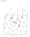
- Fig. 7 is a view for explaining the principle of working.
- a laser beam 8 is irradiated to the resin substrate 5 and the laser beam 8 is incident on the glass bead 7, the laser beam 8 refracts in plurality of times within the glass bead 7 depending upon an angle of incidence on the glass bead 7.
- the laser beam 8 loses its energy at an interface 9 between the glass bead 7 and the resin.
- the energy loss turns into heat to cause heat generation.
- the heat generating action causes fusion in the glass bead 7 and its periphery.
- thermal conductivity is worsened by the existence of glass bead 7 to reduce the diffusion of heat.
- removal is only in the region irradiated by the laser beam 8. Because the phenomenon takes place continuously in the region being irradiated by the laser beam 8, a desired linear form of hole working is realized avoiding the uneven form of penetration hole.
- the glass bead 7 is excessively large in size for a wavelength of the laser beam 8 the diffusion of heat takes place only within the glass bead 7, thus making impossible to achieve favorable hole working. Meanwhile, where the glass bead 7 is excessively small for a wavelength of the laser beam 8, no energy absorption occurs in the glass bead 7, making impossible to achieve favorable hole working. On the other hand, where the diameter of glass bead 7 is in a size of a half to 10 times of a wavelength of the laser beam 8, sufficient light absorption and heat generation take place for hole working thus making possible to favorable hole working.
- this embodiment can work a resin substrate generally difficult in favorable hole working by the use of an inexpensive YAG laser, thereby enabling resin substrate working excellent in mass producibility. Consequently, it is possible to obtain, at low cost, a resin substrate extremely low in dielectric constant and loss preferable as a high-frequency circuit substrate for micro-or-millimeter wave applications. Therefore, the use of the resin substrate provides a high-frequency circuit extremely low in heat loss.
- the resin substrate in this embodiment can be favorably worked at low cost similarly to a YAG laser,. by the use of an excimer laser, such as an ArF laser a KrF laser and an F 2 laser, besides a YAG laser.
- an excimer laser such as an ArF laser a KrF laser and an F 2 laser
- Fig. 8 shows a typical view that a glass fiber is contained in a resin substrate to improve YAG laser workability.
- Fig. 8A is a sectional view in a state of prior to laser working while Fig. 8B is a sectional view in a state of after laser working.
- a penetration hole 6 is formed nearly in a straight-line form extending along a direction of incidence of the laser beam 8.
- the sectional diameter of the glass fiber 10 is desirably a half to 10 times of a wavelength of laser light, particularly nearly the same as a wavelength of laser light.
- YAG laser workability is improved by containing a glass fiber 10 in the resin substrate 5 is as follows. Namely, when irradiating a laser light 8, absorption of laser light 8 takes place in the glass fiber 10 itself and at an interface between the glass fiber 10 and the resin of resin substrate 5 rather than in the other region. As a result, the heat of fusion occurs much more than in the other region.
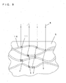
- Fig. 9 is a view for explaining the principle of working.
- a laser beam 8 is irradiated to the resin substrate 5 and the laser beam 8 is incident on the glass fiber 10, the laser beam 8 refracts in plurality of times within the glass fiber 10.
- the laser beam 8 loses its energy at the interface 11 between the glass fiber 10 and the resin.
- the energy loss turns into heat to cause heat generation.
- the heat generating action causes fusion in the glass fiber 10 and its periphery.
- removal is only in the region irradiated by the laser beam 8. Because the phenomenon takes place continuously in the region being irradiated by the laser beam 8, a desired form of worked hole is realized avoiding an uneven form of penetration hole.
- the glass fiber 10 herein is excessively large in sectional diameter size for a wavelength of the laser beam 8, the diffusion of heat occurs only within the glass fiber 10, thus making impossible to achieve favorable worked hole. Meanwhile, where the glass fiber 10 in its sectional diameter is excessively small for a wavelength of the laser beam 8, no energy absorption occurs in the glass fiber 10, making impossible to achieve favorable worked hole. On the other hand, in the case that the sectional diameter of glass fiber 10 is in a size of a half to 10 times of a wavelength of the laser beam 8, sufficient light absorption and heat generation take place for cutting. This makes it possible to work a hole such that fibers of the glass fiber 10 do not leave.
- this embodiment can work a resin substrate generally difficult in favorable hole working by the use of an inexpensive YAG laser, thereby enabling resin substrate working excellent in mass producibility. Consequently, it is possible to obtain, at low cost, a resin substrate extremely low in dielectric constant and loss preferable as a high-frequency circuit substrate for micro-or- millimeter wave applications. Therefore, the use of the resin substrate provides a high-frequency circuit extremely low in heat loss.
- the resin substrate in this embodiment also can be favorably worked at low cost similarly to a YAG laser, by the use of an excimer laser, such as an ArF laser, a KrF laser and an F 2 laser, besides a YAG laser.
- an excimer laser such as an ArF laser, a KrF laser and an F 2 laser
- Fig. 10 shows one form of a semiconductor package structure using a dielectric substrate laser-worked in the invention.
- This embodiment is an example using, as a dielectric substrate, a quartz substrate containing bubbles.
- a thin insulator 27 is formed over a surface of a quartz substrate 21 mixed with bubbles, on which is formed a pattern of electrical interconnection 24a.
- the thin insulator 27 will be detailed later.
- a pattern of electrical interconnection 24b is formed on the other surface of the quartz substrate 21.
- the electrical interconnections 24a, 24b are connected together by an electrical interconnection 24c buried in a penetration hole opened in the quartz substrate 21 by the method of Embodiment 1 or 2.
- a semiconductor device 23 is arranged on the electric interconnection 24a and connected to the electrical interconnection 24a by a wire 25.
- a metal-make lid 22 is provided covering the semiconductor device 23 on the quartz substrate 21, in order for electromagnetic shield and hermetic seal.
- the lid 22 is bonded by a conductive adhesive 26 in order to be electrically connected to the quartz substrate 21.
- a space 28, formed between the quartz substrate 21 and the lid 22, is filled and hermetically sealed with a gas less reactive with other materials, e.g. vacuum or an inert gas of helium (He), argon (Ar) or the like or nitrogen (N 2 ).
- a semiconductor package can be realized which is well in high frequency characteristic, cheap in price and high in reliability.
- the reason why a semiconductor package having such a high frequency characteristic and low price lies in that the present embodiment employs a quartz substrate 21 mixed with bubbles in contrast to the general semiconductor package using an alumina substrate structure. This is because, as noted before, the quartz substrate 21 mixed with bubbles is superior in highfrequency characteristic to the alumina substrate and, moreover, is low in working cost in laser working.
- the amount of mixing bubbles is preferably adjusted within a range of volume content ratio of 5% to 50% because of the reason noted in Embodiment 1.
- the obtainable electric characteristic can be suppressed in variation rather than the case of containing bubbles uneven in diameter. Furthermore, it is possible to considerably decrease the concavo-convex in a quartz surface of the quartz substrate 21 after being worked by using a laser.
- the laser for laser working is preferably a YAG or excimer laser in consideration of working cost, it may use a CO 2 laser or semiconductor diode laser as was explained in Embodiment 1.
- the metal-make lid 22 is electrically grounded with the electric interconnection 24a on the quartz substrate 21 by a conductive adhesive 26. Accordingly, because the unwanted electromagnetic wave given off from the semiconductor device 23 is prevented from radiating and, conversely, the unwanted electromagnetic wave from the external is prevented from intruding, the high-frequency characteristic is further improved. In this case, the lid 22 even if structured of an insulator coated with a metal film other than the metal-make one can obtain the similar effect.
- the reliability as semiconductor package is secured by hermetically sealing the interior of the package in a vacuum state or with an inert gas of helium(He), argon (Ar) or the like or nitrogen (N 2 ).
- This embodiment has a thin insulator 27 arranged on the quartz substrate 21 in order to realize hermetic seal. This is to prevent against the lower in air-tightness due to containment of bubbles in the quartz substrate 21.
- the thin insulator 27 is an organic substance, e.g. polimide, benzocyclobuthene and liquid-crystal polymer.
- the thin insulator 27 can be formed by applying an insulator in a solution state to over the quartz crystal 21 by spin coating, by laminating a pre-formed insulator 27 in a sheet form by a laminator or by pressing it while applying heat.
- the thin insulator 27 is formed extremely thin, i.e. 5 - 30 ⁇ m, as compared to the quartz substrate 21. This will not interfere with the penetration working in the quartz substrate 21 by laser working or the like. Meanwhile, the thin insulator 27 if formed thin of glass as an inorganic substance formable by spin coating (spin-on-glass called SOG or the like), besides of an organic substance, can obtain the similar effect.
- a small metal projection called bump may be formed on an electrode of the semiconductor device 23 or on the electrical interconnection 24a on the substrate end thereby connecting between the semiconductor device 23 and the electrical interconnection 24a.
- the mounting method of such a semiconductor device 23 generally uses a technique called flip-chip mounting.
- flip-chip mounting Because bump height is smaller than the wire length of wire connection, it is possible to shorten the connection distance between the semiconductor device 23 and the quartz substrate 21 and hence suppress a parasitic inductance component from occurring. This, accordingly, makes it possible to fabricate a semiconductor package higher in performance.
- the quart substrate 21 can similarly use a quartz substrate mixed with bubbles in a size of a half to 10 times of a laser light wavelength as explained in Embodiment 2, besides a quartz substrate randomly mixed with bubbles in a size of 1 - 90 ⁇ m as explained in Embodiment 1. Meanwhile, in the case of using a resin substrate mixed with a fine particular matter,'such as a glass bead, or a glass fiber as explained in Embodiments 3 and 4, a semiconductor package can be obtained having the similar operation effect.
- Fig. 11 shows another embodiment of a semiconductor package structure employing a dielectric substrate laser-worked in the invention.
- Fig. 11A is a plan view of a semiconductor package as viewed from above while Fig. 11B is a sectional view taken on line A-A' in Fig. 11A.
- the difference from Fig. 10 lies in that the electrical interconnection 24 of the semiconductor package itself is arranged only on the upper surface of the quartz substrate 21 while, although not shown, the penetration hole in the dielectric substrate 21 is utilized for connection to another semiconductor package or component.
- a high-frequency circuit for micro-or-millimeter wave applications was fabricated as a semiconductor package of Embodiments 5 and 6.
- This high-frequency circuit because low in substrate dielectric constant and loss, can reduce the heat loss on a transmission line and the heat generation on the substrate. Furthermore, because the substrate can be inexpensively laser-worked into favorable worked shape, it is possible to manufacture a circuit high in function and excellent in mass producibility.
- the high-frequency circuit applicable to wireless terminals, wireless base stations or radar devices, can provide a mass-producible device having high function.
Landscapes
- Physics & Mathematics (AREA)
- Engineering & Computer Science (AREA)
- Optics & Photonics (AREA)
- Manufacturing & Machinery (AREA)
- Microelectronics & Electronic Packaging (AREA)
- Condensed Matter Physics & Semiconductors (AREA)
- General Physics & Mathematics (AREA)
- Electromagnetism (AREA)
- Laser Beam Processing (AREA)
- Shielding Devices Or Components To Electric Or Magnetic Fields (AREA)
Abstract
Description
loss = coefficient × frequency of a circuit under handled × (dielectric coefficient of the substrate 101)1/2 × dielectric loss of the substrate 101 (dielectric tangent).
The loss in this case turns into heat energy, causing a phenomenon to generate heat upon the
| Working Conditions of Bubble-contained Quartz Glass by Various Lasers | |||||
| Laser scheme | Wavelength | output form of Laser | Power | Shots | |
| RF excited CO2 laser | 10.6µm | Pulse (pulse width: 10msec) | | 1 shot | |
| YAG laser | 1.06µm | Pulse (pulse width: 500 µsec.) | 1.1 | 5 shots | |
| Semiconductor diode laser | 0.81µm | | 470W | 3 seconds |
| Working Conditions on Bubble-containing Glass by a YAG Laser | ||||
| Bubble size | Volume content ratio of bubbles | YAG laser workability | Corresponding figure | |
| Sample A | 0.1∼0.5µm | Approx. 10% | Only crater formed | Fig. 4 |
| Sample B | 2.0∼5.0µm | Approx. 5% | Penetration hole formed | Fig. 3 |
| | 100∼200µm | Approx. 12% | Not formed | ---- |
Claims (44)
- A dielectric substrate for laser working characterized in that a dielectric substrate contains a substance having a size of a half to 10 times of a wavelength of laser light and different in refractive index from a material of said dielectric substrate.
- A dielectric substrate according to claim 1, wherein the substance different in refractive index from a material of said dielectric substrate is in a volume content ratio of 5% - 50%.
- A dielectric substrate according to claim 1, wherein the dielectric substrate material is glass or resin.
- A dielectric substrate according to claim 1, wherein the substance different in refractive index from a material of said dielectric substrate is bubble.
- A dielectric substrate according to claim 3, wherein the resin is any one selected from polyimide, liquid-crystal polymer, benzocyclobutene and polyphenylene ether.
- A dielectric substrate according to claim 1, wherein said dielectric substrate is of resin and the substance different in refractive index from a material of said dielectric substrate is a fine particle or a fiber.
- A dielectric substrate according to claim 6, wherein a diameter of the fine particle or a sectional diameter of the fiber has a size substantially the same as a laser light wavelength.
- A dielectric substrate according to claim 6, wherein the fine particle is a glass bead.
- A dielectric substrate according to claim 6, wherein the fiber is a glass fiber.
- A method for working a dielectric substrate characterized in that by a laser is formed a dielectric substrate containing a substance having a size of a half to 10 times of a wavelength of laser light and different in refractive index from a material of said dielectric substrate.
- A method according to claim 10, wherein the laser is a YAG laser or an excimer laser.
- A method according to claim 10, wherein the laser is a YAG laser using, as laser light, any of a basic wave, a second harmonic and a third harmonic.
- A method according to claim 10, wherein the excimer laser is any one selected from an ArF laser, a KrF laser and an F2 laser.
- A semiconductor package having a semiconductor device provided on a substrate and sealed within a container, the semiconductor package characterized in that said substrate provided with said semiconductor device is a quartz substrate and said quartz substrate contains bubbles.
- A semiconductor package according to claim 14, wherein the bubbles contained in said quartz substrate are arbitrarily controlled in amount.
- A semiconductor package according to claim 14, wherein the bubbles contained in said quartz substrate are in a size of 10 µm or smaller.
- A semiconductor package according to claim 14, wherein said substrate provided with said semiconductor device is a quartz substrate containing bubbles and formed thereon with a thin insulator.
- A semiconductor package according to claim 17, wherein said thin insulator is an organic matter.
- A semiconductor package having a semiconductor device provided on a substrate and sealed within a container, the semiconductor package characterized in that said substrate provided with said semiconductor device is a dielectric substrate and said dielectric substrate contains a substance having a size of a half to 10 times of a wavelength of laser light and different in refractive index from a material of said dielectric substrate.
- A semiconductor package according to claim 19, wherein said dielectric substrate is a quartz substrate and the material different in refractive index from a material of said dielectric substrate is bubbles.
- A semiconductor package according to claim 20, wherein the bubbles contained in said quartz substrate are in a volume content ratio of 5% - 50%.
- A semiconductor package according to claim 20, wherein the bubbles contained in said quartz substrate are in a size of a half to 10 times of a laser wavelength.
- A semiconductor package according to claim 14, wherein said semiconductor device is flip-chip-mounted on said quartz substrate.
- A semiconductor package according to claim 23, wherein an electromagnetic shielding cap is arranged covering said semiconductor device on said quartz substrate.
- A semiconductor package according to claim 24, wherein said electromagnetic shielding cap is a metal or insulator coated with a metal film.
- A semiconductor package according to claim 19, wherein the dielectric substrate material is a resin of any one selected from polyimide, liquid-crystal polymer, benzocyclobutene and polyphenylene ether.
- A semiconductor package according to claim 19, wherein said dielectric substrate is of resin and the substance different in refractive index from said dielectric substrate is a fine particle or a fiber.
- A semiconductor package according to claim 27, wherein a diameter of the fine particle or a sectional diameter of the fiber has a size substantially the same as a laser light wavelength.
- A semiconductor package according to claim 28, wherein the fine particle is a glass bead.
- A semiconductor package according to claim 28, wherein the fiber is a glass fiber.
- A semiconductor package according to claim 19, wherein said dielectric substrate is of resin to have said semiconductor device flip-chip-mounted on said resin substrate.
- A semiconductor package according to claim 31, wherein an electromagnetic shielding cap is arranged covering said semiconductor device on the resin substrate.
- A semiconductor package according to claim 24, wherein said electromagnetic shielding cap is a metal or insulator coated with a metal film.
- A method for manufacturing a semiconductor package characterized in that a thin insulator layer is formed on a quartz substrate mixed with bubbles to provide thereon a semiconductor device and sealed within a container.
- A method according to claim 34, the thin insulator layer is formed by applying an insulator liquid material on a quartz substrate.
- A method according to claim 34, the thin insulator layer is formed by laminating an insulator sheet material on a quartz substrate.
- A method according to claim 34, the thin insulator layer is formed by pressing an insulator sheet material on a quartz substrate.
- A method according to claim 34, further comprising a step of forming a first electrical interconnect pattern on said thin insulator layer, a step of providing a semiconductor device on a part of the first electrical interconnection pattern, a step of forming a second electrical interconnection pattern on the other surface of said quartz substrate, a step of forming a penetration hole in said quartz substrate by a laser, a step of passing a third electrical interconnection through said penetration hole, and a step of connecting said first electrical interconnection pattern and said second electrical interconnection pattern through a third electrical interconnection.
- A method according to claim 38, wherein the laser is any one selected from a CO2 laser, a YAG laser, an excimer laser and a semiconductor diode laser.
- A method for manufacturing a semiconductor package comprising: a step of forming a penetration hole by a laser in a dielectric substrate containing a substance having a size of a half to 10 times of a laser light wavelength and different in refractive index from a material of said dielectric substrate, a step of forming a first electrical interconnection pattern on a first surface of said dielectric substrate, a step of providing a semiconductor device on a part of the first electrical interconnection pattern, a step of forming a second electrical interconnection pattern on the other surface of said dielectric substrate, a step of forming a penetration hole by a laser in said dielectric substrate, a step of passing a third electrical interconnection through said penetration hole, a step of connecting between said first electrical interconnection pattern and said second electrical interconnection pattern through said third electrical interconnection, and a step of sealing said semiconductor device in a container.
- A method according to claim 40, wherein the laser is a YAG laser or an excimer laser.
- A high-frequency circuit having a semiconductor device provided on a substrate and sealed in a container, the high-frequency circuit characterized in that said substrate provided with said semiconductor device is a quartz substrate and said quartz substrate contains bubbles in a size of a half to 10 times of a laser light wavelength.
- A high-frequency circuit having a semiconductor device provided on a substrate and sealed within a container, the high-frequency circuit characterized in that said substrate provided with said semiconductor device is a resin substrate and said resin substrate contains a glass bead or a glass fiber.
- A high-frequency circuit according to claim 43, wherein a diameter of the glass bead or a sectional diameter of the glass fiber has a size substantially the same as a laser light wavelength.
Applications Claiming Priority (4)
| Application Number | Priority Date | Filing Date | Title |
|---|---|---|---|
| JP2001082155 | 2001-03-22 | ||
| JP2001082155 | 2001-03-22 | ||
| JP2002036514 | 2002-02-14 | ||
| JP2002036514A JP2002359445A (en) | 2001-03-22 | 2002-02-14 | Dielectric substrate for laser processing, method of processing the same, and semiconductor package and method of manufacturing the same |
Publications (2)
| Publication Number | Publication Date |
|---|---|
| EP1246325A2 true EP1246325A2 (en) | 2002-10-02 |
| EP1246325A3 EP1246325A3 (en) | 2004-08-25 |
Family
ID=26611772
Family Applications (1)
| Application Number | Title | Priority Date | Filing Date |
|---|---|---|---|
| EP02006503A Withdrawn EP1246325A3 (en) | 2001-03-22 | 2002-03-18 | Laser working dielectric substrate and method for working same and semiconductor package and method for manufacturing same |
Country Status (6)
| Country | Link |
|---|---|
| US (2) | US20020175396A1 (en) |
| EP (1) | EP1246325A3 (en) |
| JP (1) | JP2002359445A (en) |
| KR (1) | KR20020075272A (en) |
| CN (1) | CN1376554A (en) |
| TW (1) | TW536773B (en) |
Cited By (1)
| Publication number | Priority date | Publication date | Assignee | Title |
|---|---|---|---|---|
| WO2004075336A1 (en) * | 2003-02-21 | 2004-09-02 | Matsushita Electric Industrial Co., Ltd. | High frequency circuit |
Families Citing this family (23)
| Publication number | Priority date | Publication date | Assignee | Title |
|---|---|---|---|---|
| US7170148B2 (en) * | 2003-07-02 | 2007-01-30 | Analog Devices, Inc. | Semi-fusible link system for a multi-layer integrated circuit and method of making same |
| GB2405249B (en) * | 2003-08-22 | 2007-03-07 | Ipwireless Inc | Holder for module and method therefor |
| JP4642634B2 (en) * | 2005-10-31 | 2011-03-02 | パナソニック株式会社 | Manufacturing method of acoustic sensor |
| CN100397669C (en) * | 2006-08-07 | 2008-06-25 | 陈盈君 | A preparation method of LED light source using low temperature co-fired ceramics designed by thermoelectric separation |
| CN103465525B (en) | 2006-12-27 | 2015-10-21 | 日立化成株式会社 | The base material with conductor layer pattern of intaglio plate and this intaglio plate of use |
| US7874846B2 (en) * | 2007-06-22 | 2011-01-25 | Seagate Technology Llc | Hermetically sealed liquid crystal polymer interconnect |
| US20090108436A1 (en) * | 2007-10-31 | 2009-04-30 | Toshio Fujii | Semiconductor package |
| JP2009158841A (en) * | 2007-12-27 | 2009-07-16 | Hitachi Chem Co Ltd | Conductive substrate for plating, manufacturing method thereof and method of manufacturing substrate with conductive layer pattern, substrate with conductive layer pattern, and light transparent electromagnetic wave shielding member |
| JP5380724B2 (en) * | 2008-03-27 | 2014-01-08 | 新光電気工業株式会社 | Optical semiconductor device package and manufacturing method thereof |
| JP4666028B2 (en) * | 2008-03-31 | 2011-04-06 | カシオ計算機株式会社 | Semiconductor device |
| US20110017257A1 (en) * | 2008-08-27 | 2011-01-27 | Stion Corporation | Multi-junction solar module and method for current matching between a plurality of first photovoltaic devices and second photovoltaic devices |
| KR101580925B1 (en) * | 2009-04-28 | 2015-12-30 | 삼성전자주식회사 | Chip-on-board type package |
| JP5306076B2 (en) * | 2009-06-29 | 2013-10-02 | 京セラ株式会社 | Junction structure, method for manufacturing junction structure, photoelectric conversion device, and method for manufacturing photoelectric conversion device |
| DE102010055627A1 (en) * | 2010-12-22 | 2012-06-28 | Epcos Ag | Electrical module for insertion by automatic insertion machines by generating a vacuum |
| CN103681593A (en) * | 2013-12-02 | 2014-03-26 | 江苏省宜兴电子器件总厂 | Leadless ceramic chip carrier packaging structure and process for manufacturing same |
| US10276368B2 (en) * | 2014-10-03 | 2019-04-30 | Nippon Sheet Glass Company, Limited | Method for producing glass substrate with through glass vias and glass substrate |
| CN106163101A (en) * | 2015-04-17 | 2016-11-23 | 欣兴电子股份有限公司 | Dielectric layer for circuit substrate |
| DE102015110422A1 (en) * | 2015-06-29 | 2016-12-29 | Schott Ag | Laser processing of a multiphase transparent material, as well as multiphase composite material |
| CN107926111A (en) * | 2015-08-21 | 2018-04-17 | 康宁股份有限公司 | Method for the continuous manufacture of features in flexible substrates and products related thereto |
| CN107809055A (en) * | 2017-12-14 | 2018-03-16 | 长春理工大学 | A kind of high-power semiconductor laser chip welding and assembling method |
| WO2019156051A1 (en) * | 2018-02-08 | 2019-08-15 | 株式会社村田製作所 | High-frequency module |
| IT201900006736A1 (en) * | 2019-05-10 | 2020-11-10 | Applied Materials Inc | PACKAGE MANUFACTURING PROCEDURES |
| US11676832B2 (en) | 2020-07-24 | 2023-06-13 | Applied Materials, Inc. | Laser ablation system for package fabrication |
Family Cites Families (4)
| Publication number | Priority date | Publication date | Assignee | Title |
|---|---|---|---|---|
| JPH07335994A (en) * | 1994-06-08 | 1995-12-22 | Hitachi Chem Co Ltd | Interconnection board |
| US5642262A (en) * | 1995-02-23 | 1997-06-24 | Altera Corporation | High-density programmable logic device in a multi-chip module package with improved interconnect scheme |
| JP3883233B2 (en) * | 1996-07-15 | 2007-02-21 | 信越石英株式会社 | Method for producing quartz glass foam |
| WO1998020528A1 (en) * | 1996-11-08 | 1998-05-14 | W.L. Gore & Associates, Inc. | METHOD FOR IMPROVING RELIABILITY OF THIN CIRCUIT SUBSTRATES BY INCREASING THE Tg OF THE SUBSTRATE |
-
2002
- 2002-02-14 JP JP2002036514A patent/JP2002359445A/en active Pending
- 2002-03-13 US US10/099,193 patent/US20020175396A1/en not_active Abandoned
- 2002-03-18 EP EP02006503A patent/EP1246325A3/en not_active Withdrawn
- 2002-03-21 TW TW091105426A patent/TW536773B/en not_active IP Right Cessation
- 2002-03-21 KR KR1020020015258A patent/KR20020075272A/en not_active Withdrawn
- 2002-03-22 CN CN02107946A patent/CN1376554A/en active Pending
- 2002-09-17 US US10/245,465 patent/US20030020149A1/en not_active Abandoned
Cited By (1)
| Publication number | Priority date | Publication date | Assignee | Title |
|---|---|---|---|---|
| WO2004075336A1 (en) * | 2003-02-21 | 2004-09-02 | Matsushita Electric Industrial Co., Ltd. | High frequency circuit |
Also Published As
| Publication number | Publication date |
|---|---|
| TW536773B (en) | 2003-06-11 |
| EP1246325A3 (en) | 2004-08-25 |
| CN1376554A (en) | 2002-10-30 |
| JP2002359445A (en) | 2002-12-13 |
| US20020175396A1 (en) | 2002-11-28 |
| KR20020075272A (en) | 2002-10-04 |
| US20030020149A1 (en) | 2003-01-30 |
Similar Documents
| Publication | Publication Date | Title |
|---|---|---|
| EP1246325A2 (en) | Laser working dielectric substrate and method for working same and semiconductor package and method for manufacturing same | |
| US10756003B2 (en) | Inorganic wafer having through-holes attached to semiconductor wafer | |
| JP2001354439A (en) | Glass substrate processing method and high frequency circuit manufacturing method | |
| US7306689B2 (en) | Optical waveguide and method for producing same | |
| CA2177276C (en) | Method for fabricating self-assembling microstructures | |
| KR20010042981A (en) | Method For Machining Work By Laser Beam | |
| CA2177219A1 (en) | Method and apparatus for fabricating self-assembling microstructures | |
| US12100890B2 (en) | Liquid crystal antenna and manufacturing method therefor | |
| JP2022512609A (en) | Systems and methods for forming displays with embedded side electrodes | |
| US12394690B2 (en) | Systems and methods of nano-particle bonding for electronics cooling | |
| US20250259901A1 (en) | Semiconductor devices and methods of manufacturing semiconductor devices | |
| US20180218997A1 (en) | Method for direct bonding with self-alignment using ultrasound | |
| US20250087500A1 (en) | Method for preparing fcbga package substrate | |
| KR100691708B1 (en) | Method for manufacturing circuit element, method for manufacturing electronic element, circuit board, electronic device, and electro-optical device | |
| JP2010034260A (en) | Wiring substrate, method of manufacturing the same, and mounting structure | |
| CN1180461C (en) | Composite high-density packaging substrate and forming method thereof | |
| Zhang et al. | Cornerstone of Next-Generation 3D Integration: Structures, Processes, and Applications of TGV | |
| US20250070528A1 (en) | Structured wafer and optoelectronic component produced therewith | |
| CN121367117A (en) | Step type substrate suitable for high-speed laser encapsulation | |
| KR20010030491A (en) | Target for providing film on semiconductor substrate using laser emission and method of making the same | |
| WO2025186425A1 (en) | Component carrier with resin-embedded component, and manufacturing method | |
| Sun et al. | Microvia formation with lasers | |
| Guo et al. | Fabrication of Full Glass Antenna-in-Package by Laser Transmission Welding | |
| CN121908460A (en) | Component carrier and method for producing the same | |
| JP2003332811A (en) | Microwave integrated circuit, method of manufacturing the same, and wireless device |
Legal Events
| Date | Code | Title | Description |
|---|---|---|---|
| PUAI | Public reference made under article 153(3) epc to a published international application that has entered the european phase |
Free format text: ORIGINAL CODE: 0009012 |
|
| AK | Designated contracting states |
Kind code of ref document: A2 Designated state(s): AT BE CH CY DE DK ES FI FR GB GR IE IT LI LU MC NL PT SE TR |
|
| AX | Request for extension of the european patent |
Free format text: AL;LT;LV;MK;RO;SI |
|
| PUAL | Search report despatched |
Free format text: ORIGINAL CODE: 0009013 |
|
| AK | Designated contracting states |
Kind code of ref document: A3 Designated state(s): AT BE CH CY DE DK ES FI FR GB GR IE IT LI LU MC NL PT SE TR |
|
| AX | Request for extension of the european patent |
Extension state: AL LT LV MK RO SI |
|
| AKX | Designation fees paid |
Designated state(s): DE FR GB |
|
| RBV | Designated contracting states (corrected) |
Designated state(s): DE FR GB |
|
| STAA | Information on the status of an ep patent application or granted ep patent |
Free format text: STATUS: THE APPLICATION IS DEEMED TO BE WITHDRAWN |
|
| 18D | Application deemed to be withdrawn |
Effective date: 20050226 |