EP1246010A2 - Photomask manufacturing method, photomask manufactured by said manufacturing method, and semiconductor device method using said photomask - Google Patents
Photomask manufacturing method, photomask manufactured by said manufacturing method, and semiconductor device method using said photomask Download PDFInfo
- Publication number
- EP1246010A2 EP1246010A2 EP02007238A EP02007238A EP1246010A2 EP 1246010 A2 EP1246010 A2 EP 1246010A2 EP 02007238 A EP02007238 A EP 02007238A EP 02007238 A EP02007238 A EP 02007238A EP 1246010 A2 EP1246010 A2 EP 1246010A2
- Authority
- EP
- European Patent Office
- Prior art keywords
- pattern
- photomask
- layout
- area
- manufacturing
- Prior art date
- Legal status (The legal status is an assumption and is not a legal conclusion. Google has not performed a legal analysis and makes no representation as to the accuracy of the status listed.)
- Granted
Links
Images




Classifications
-
- G—PHYSICS
- G03—PHOTOGRAPHY; CINEMATOGRAPHY; ANALOGOUS TECHNIQUES USING WAVES OTHER THAN OPTICAL WAVES; ELECTROGRAPHY; HOLOGRAPHY
- G03F—PHOTOMECHANICAL PRODUCTION OF TEXTURED OR PATTERNED SURFACES, e.g. FOR PRINTING, FOR PROCESSING OF SEMICONDUCTOR DEVICES; MATERIALS THEREFOR; ORIGINALS THEREFOR; APPARATUS SPECIALLY ADAPTED THEREFOR
- G03F1/00—Originals for photomechanical production of textured or patterned surfaces, e.g., masks, photo-masks, reticles; Mask blanks or pellicles therefor; Containers specially adapted therefor; Preparation thereof
- G03F1/36—Masks having proximity correction features; Preparation thereof, e.g. optical proximity correction [OPC] design processes
-
- H—ELECTRICITY
- H10—SEMICONDUCTOR DEVICES; ELECTRIC SOLID-STATE DEVICES NOT OTHERWISE PROVIDED FOR
- H10P—GENERIC PROCESSES OR APPARATUS FOR THE MANUFACTURE OR TREATMENT OF DEVICES COVERED BY CLASS H10
- H10P76/00—Manufacture or treatment of masks on semiconductor bodies, e.g. by lithography or photolithography
-
- Y—GENERAL TAGGING OF NEW TECHNOLOGICAL DEVELOPMENTS; GENERAL TAGGING OF CROSS-SECTIONAL TECHNOLOGIES SPANNING OVER SEVERAL SECTIONS OF THE IPC; TECHNICAL SUBJECTS COVERED BY FORMER USPC CROSS-REFERENCE ART COLLECTIONS [XRACs] AND DIGESTS
- Y10—TECHNICAL SUBJECTS COVERED BY FORMER USPC
- Y10S—TECHNICAL SUBJECTS COVERED BY FORMER USPC CROSS-REFERENCE ART COLLECTIONS [XRACs] AND DIGESTS
- Y10S438/00—Semiconductor device manufacturing: process
- Y10S438/942—Masking
Definitions
- the present invention relates to a method of manufacturing a photomask for correcting the design data of the layout pattern of a photomask for transferring a predetermined optical image pattern onto a substrate, a photomask manufactured by using the layout pattern corrected by the correcting method, and a method for manufacturing a semiconductor device using the photomask thus manufactured.
- the miniaturization also proceeds in the pattern size of the photomask providing the original plate of the circuit pattern.
- the demands for accuracy are becoming strict and strict.
- various corrections such as the OPC (Optical Proximity Correction) have come to be applied to the design pattern in the device process in order to achieve an accuracy of several nanometers.
- the accuracy of the photomask is a very important factor in the device process.
- the process size is changed depending on the pattern aperture rate or the pattern density by the micro loading effect in the step of the developing process or the dry etching process.
- the size of the pattern on the photomask is several times as large as the size of the image transferred onto the wafer, with the result that the pattern aperture rate of the photomask greatly differs depending on the layer, which to increases the variations in size generated by the difference in the aperture rate.
- the difference in density of the patterns among the different regions on the photomask is increased by the diversification of the devices.
- the change in size caused by the micro loading effect has obstructed the improvements in the dimensional accuracy and positional accuracy corresponding to the demands for the miniaturization.
- the layout data for photomask writing system is basically equal to the initial design data, and the pattern size drawn by photomask writing system is equal to the desired pattern size. It should be noted, however, that, where the finish size is shifted from the design data because of, for example, the decrease in the shot connection in EB (electron beam) exposure system using VSB (variable shaped beam) method and the improvements in the pattern image quality and the dimensional accuracy, a predetermined photomask data bias(resize) is given to the layout data for photomask writing system relative to the design data. In any case, photomask data bias is uniform relative to a certain process regardless of the pattern aperture rate.
- the etching rates for these patterns differ from each other, which gives rise to a difference in the pattern shape and to a difference of scores of nanometers in the final size.
- the photomask is discarded as a defective photomask, and a new photomask is remade again by controlling and changing the process conditions. In this fashion, similar steps are repeated until a photomask satisfying the desired standards is obtained.
- the aperture rate differs if the patterns differ from each other in the line width and the chip area.
- a change in the process size also takes place similarly.
- the difference in size between the patterns is increased to reach scores of nanometers.
- the change in the process size also affects the positional accuracy and the accuracy in the XY difference. It is difficult to control such a large difference in size by adjusting the process conditions alone, and it is necessary to repeat the preparation many times by adjusting the process conditions. Depending on the process conditions, the process margin was lowered, which brought about drawbacks such as an increase in defects.
- a method of manufacturing a photomask for correcting a layout pattern of a photomask in which are arranged a light transmitting pattern portion and a light shielding pattern portion for forming an optical image pattern on the surface of a substrate comprising calculating a pattern area ratio, which is a ratio of the light transmitting pattern portion or the light shielding pattern portion to an area of the photomask from the design data of a given layout pattern of the photomask, and a pattern density, which is a ratio of the light transmitting pattern portion or light shielding pattern portion within the region to the area of the region extracted from the given layout pattern; estimating from the calculated pattern area ratio and the pattern density the size of a pattern, positional accuracy or the XY difference, covering the case where the pattern is formed on the photomask by using the design data of the given layout pattern; and imparting the amount of correction to the design data of the given layout pattern based on the estimated pattern size, positional accuracy or the XY difference.
- a method of manufacturing a photomask for correcting the layout pattern of a photomask in which a light transmitting pattern portion and a light shielding pattern portion are formed for forming a predetermined optical image pattern on the surface of a substrate comprising, calculating a pattern area ratio, which is a ratio of the area of the light transmitting pattern portion or the light shielding pattern portion to the area of a photomask, and a pattern density, which is a ratio of the area of the light transmitting pattern portion or the light shielding pattern portion within the region to the area of the region extracted from the given layout pattern based on given design data of the layout pattern of the photomask; estimating the positional accuracy of the formed pattern from the calculated pattern area ratio and the pattern density, covering the case where a pattern is formed in the photomask by using given design data of the layout pattern; and imparting a correction amount to the given layout pattern based on the estimated positional accuracy.
- a method of manufacturing a photomask for correcting the layout pattern of the photomask in which a light transmitting pattern portion and a light shielding pattern portion are arranged for forming a predetermined optical image pattern on the surface of a substrate comprising calculating a pattern area ratio, which is a ratio of the area of the light transmitting pattern portion or the light shielding pattern portion to the area of the photomask, from the design data of a given layout pattern of the photomask, and a pattern density, which is a ratio of the area of the light transmitting pattern portion or the light shielding pattern portion within the region to the area of the region extracted from the given layout pattern; estimating the XY difference of the formed pattern from the calculated pattern area ratio and the pattern density, covering the case where a pattern is formed on the photomask by using the design data of the imparted layout pattern; and imparting a correction amount to the imparted layout pattern based on the estimated XY difference.
- the first embodiment is directed to a method of manufacturing a photomask pattern for a memory device represented by DRAM, in which the pattern density is almost uniform.
- FIG. 1 is a block diagram schematically showing the construction of an apparatus for converting the photomask layout pattern.
- a reference numeral 101 denotes photomask layout data that is to be corrected
- a reference numeral 102 denotes a data bias conversion parameter calculating section for calculating the parameter required for the conversion from the photomask layout data 101 into new data
- a reference numeral 102a denotes a pattern area ratio calculating section
- a reference numeral 102b denotes a pattern density calculating section
- a reference numeral 103 denotes a layout data conversion section for correcting the photomask layout data 101 by using the parameter calculated in the data bias conversion parameter calculating section 102 and a correlation 104 referred to herein later and outputting converted photomask layout data 105.
- FIG. 2 is a flow chart showing how to derive the function relating to the first embodiment of the present invention.
- the finish size(CD value) W represents the difference between the pattern size on the photomask formed and processed on the basis of the layout data and the design size on the layout data.
- the photomask pattern area ratio C represents the ratio of the area of the light transmitting pattern portion (light shielding pattern portion) in the photomask to the area Am of the photomask.
- the pattern density D represents the ratio of the area of the light transmitting pattern portion (light shielding pattern portion) to the area of the region extracted from the photomask.
- FIGS. 3A, 3B, 3C and 3D schematically show the construction of the photomask for evaluation.
- FIG. 3A is a plan view schematically showing the entire construction of the photomask for evaluation.
- FIG. 3B is a plan view schematically showing the chip region formed in the photomask shown in FIG. 3A.
- FIGS. 3C and 3D are plan views each schematically showing the pattern for measuring the size, said pattern being formed in the chip region shown in FIG. 3B.
- a plurality of chip regions 202 are arranged in a photomask 201 for evaluation.
- a size measuring pattern region 204 having a size measuring pattern formed therein is arranged in the central portion of each chip region 202, and an aperture rate change region 203 having a different aperture rate for each photomask is formed around the size measuring pattern region 204.
- the size measuring pattern formed in the size measuring pattern region 204 is common with each chip forming region and each photomask 201 for evaluation.
- size measuring patterns 205 are formed of patterns differing from each other in the pattern density depending on the regions.
- a pattern density D of the wiring patterns is changed as shown in FIG. 3C.
- the pattern density of the holes is changed, as shown in FIG. 3D.
- the pattern density relative to regions P n (n representing the number of the extracted region) in which the pattern density is changed is represented by D n .
- the area of the light shielding film is changed for every photomask for evaluation.
- the planar pattern area ratio of each photomask can be changed by changing the aperture ratio of the aperture ratio change region.
- the size measuring pattern formed in each photomask 201 for evaluation is measured, and the finish size (CD value) W, which is the shift amount relative to the design size value, is obtained from the measured value.
- CD value the finish size
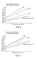
- FIGS. 4 and 5 show the correlation obtained where the processing was performed under different conditions. Where a plurality of process conditions are employed as in this case, a photomask for evaluation is manufactured for each process condition so as to obtain each correlation function f.
- the finish size W which represents the shift amount from the design size value, is used as the photomask data bias.
- the photomask data bias r which is equal to f(C, D)/2, is defined as the shift amount for the edge portion on one side.
- the photomask data bias r which is due to the definition in synthesizing the pattern data, need not be 1/2.
- Patterns of various densities are arranged in the region 204 in the layout pattern shown in FIG. 3. Therefore, in the case where the process conditions are made common by using the particular photomask, it is possible to obtain the function f common with the layout pattern having a difference in density such as the logic device and the memory-mixed device in addition to the memory device.
- the pattern area ratio Cm in the photomask plane in respect of the layout data 101 of the product photomask and the pattern density Dn within a specified region Pn, which has been extracted, are calculated in the data bias conversion parameter calculating section 102.
- the ratio of the open portion to the layout is calculated from the layout data 101, and ratio thus obtained is used as the layout pattern area ratio Cw.
- the layout pattern area ratio Cw is converted into a pattern area ratio Ca on the photomask substrate on the basis of the chip area Aw and the photomask substrate area Am.
- the pattern area ratio Cm on the photomask is obtained by adding the area ratio Cb of the various peripheral marks arranged on the photomask to the pattern area ratio Ca.
- the pattern area ratio calculating section 102a By the steps described above, it is possible for the pattern area ratio calculating section 102a to obtain the pattern area ratio Cm.
- a region including a pattern requiring the highest dimensional accuracy among the layout is extracted as a specified region P n .
- the size of the specified region P n is optional. However, it is necessary for the specified region P n to be sufficiently smaller than the chip area A w , (P n ⁇ A w ).
- the size of the extracted region is set at a level not larger than one memory cell unit.
- the pattern density calculating section 102b By the steps described above, it is possible for the pattern density calculating section 102b to obtain the pattern density D 1 .
- the pattern area ratio calculating section 102a to carry out the calculation of the pattern area ratio and for the pattern density calculating section 102b to carry out the calculation of the pattern density simultaneously or successively. Also, it is possible for any of the calculation of the pattern area ratio and the calculation of the pattern density to be carried out first.
- the photomask data bias r is obtained by substituting the pattern area ratio C m and the pattern density D 1 of the photomask obtained previously in the correlation 104 giving the photomask data bias r.
- a new photomask layout data is formed by the steps described above.
- a photomask is prepared on the basis of the converted photomask layout data 105. It is possible for the photomask thus prepared to obtain a desired finish size.
- the size of the data is corrected in advance in the photomask prepared by the method described above, it is unnecessary to adjust the dosage in the exposure step and the process conditions for every pattern so as to make it possible to ensure a process margin, to perform the treatment with a stable process, and to be low in fluctuation of the yield.
- the second embodiment of the present invention is directed to a method of manufacturing a photomask pattern for kinds of memory-mixed logic device which have a plurality of unit devices differing from each other in pattern density .
- FIG. 9 is a flow chart showing the conversion method of a photomask layout data according to the second embodiment of the present invention.
- the correlation function f in the second embodiment is derived as in the first embodiment described previously with reference to FIG. 2 and, thus, the description is omitted with respect to the steps of deriving the correlation function f in the second embodiment. Also, the steps S201 to S203 for calculating the pattern area ratio Cm shown in FIG. 9 are equal to those for the first embodiment and, thus, the description of these steps S201 to S203 is omitted.
- the photomask layout data 101 is divided into blocks for unit devices so as to obtain specified regions P 1 to P n .
- the pattern densities D 1 to D n for the specified regions P 1 to P n are calculated.
- the pattern densities D 1 to D n and the pattern area ratio Cm are substituted in the correlation 104 in the pattern data change section so as to obtain photomask data bias r 1 to r n in the specified regions P 1 to P n .
- the method according to the second embodiment of the present invention to not only a mixed logic device but also to a photomask pattern, which has a similar layout pattern and which can be divided into blocks depending on the pattern density.
- the third embodiment of the present invention is directed to a method of preparing a photomask pattern for a logic device in which the pattern density in a plane is not uniform and the layout pattern cannot be divided easily.
- FIG. 10 is a flow chart showing the change method of a photomask layout data according to the third embodiment of the present invention.
- the correlation function f in the third embodiment is derived as in the first embodiment described previously with reference to FIG. 2 and, thus, the description is omitted with respect to the steps of deriving the correlation function f in the third embodiment. Also, the steps S201 to S203 for calculating the pattern area ratio Cm shown in FIG. 10 are equal to those for the first embodiment and, thus, the description of these steps S201 to S203 is omitted.
- a pattern requiring the highest dimensional accuracy within the photomask is extracted in respect of the layout pattern, and the region within 100 ⁇ m from the extracted pattern constitutes a region P 1 . Then, the pattern density D1 in the region P 1 is calculated.
- the photomask data bias r 1 thus obtained is inputted so as to synthesize again pattern data, and a photomask is prepared by using the data after the synthesis. In this fashion, it is possible to obtain a desired finish size in respect of the logic device pattern in which the pattern density in a photomask plane is not uniform.
- the third embodiment described above a single pattern requiring the highest dimensional accuracy within the mask was extracted so as to provide the region P 1 .
- the average value of the pattern densities of the peripheral regions is used as the pattern density D1.
- the size of the peripheral region is set at 100 ⁇ m in the third embodiment described above. However, the size noted above need not be limited to 100 ⁇ m.
- the application of the method according to the third embodiment of the present invention is not limited to a logic device, and the method according to the third embodiment of the present invention can be applied to various layout patterns. Further, the third embodiment of the present invention is advantageous in that, since the data bias is unique for each layout pattern, the pattern data can be synthesized again easily.
- the method according to the third embodiment of the present invention makes it possible to obtain a desired positional accuracy or a desired XY difference accuracy with a high yield by the application of the particular method to the correction of the positional accuracy or the XY difference accuracy, like the methods according to the first and second embodiments described above.
- the present invention is not limited to the embodiments described above. In other words, the present invention can be worked in variously modified fashions within the technical scope of the present invention.
Landscapes
- Physics & Mathematics (AREA)
- General Physics & Mathematics (AREA)
- Preparing Plates And Mask In Photomechanical Process (AREA)
- Exposure And Positioning Against Photoresist Photosensitive Materials (AREA)
Abstract
Description
Claims (12)
- A method for manufacturing a photomask in which are arranged a light transmitting pattern portion and a light shielding pattern portion for forming an optical image pattern on the surface of a substrate, characterized by comprising:calculating a pattern area ratio, which is a ratio of the light transmitting pattern portion or the light shielding pattern portion to an area of the photomask from the design data of a given layout pattern of the photomask, and a pattern density, which is a ratio of said light transmitting pattern portion or light shielding pattern portion within said region to the area of the region extracted from the given layout pattern;estimating from the calculated pattern area ratio and the pattern density the size of a pattern formed in the case where the pattern is formed on the photomask by using the design data of the given layout pattern; andimparting the amount of correction to the design data of the given layout pattern based on the estimated pattern size.
- The method for manufacturing a photomask according to claim 1, characterized in that the region extracted from said layout pattern is a region including a pattern requiring the highest dimensional accuracy among the layout pattern.
- The method for manufacturing a photomask according to claim 1, characterized in that the estimation of said pattern size is performed by using any of:a first function representing the relationship between said pattern area ratio and the pattern size obtained by actually processing the photomask;a second function representing the relationship between said pattern density and the pattern size obtained by actually processing the photomask; anda third function representing the relationship between said pattern area ratio, said pattern density, and the pattern size obtained by actually processing the photomask.
- The method for manufacturing a photomask according to claim 3, characterized in that said second function and said third function are obtained by measuring the pattern sizes of photomasks for evaluation processed by using a plurality of pattern data having patterns for the size measurement having a plurality of pattern densities arranged therein and differing from each other in the pattern area ratio.
- A method for manufacturing a photomask in which a light transmitting pattern portion and a light shielding pattern portion are formed for forming a predetermined optical image pattern on the surface of a substrate, characterized by comprising:calculating a pattern area ratio, which is a ratio of the area of the light transmitting pattern portion or the light shielding pattern portion to the area of a photomask, and a pattern density, which is a ratio of the area of said light transmitting pattern portion or the light shielding pattern portion within said region to the area of the region extracted from the given layout pattern based on a given design data of the layout pattern of the photomask;estimating the positional accuracy of the formed pattern from the calculated pattern area ratio and the pattern density, covering the case where a pattern is formed in the photomask by using a given design data of the layout pattern; andimparting a correction amount to the given layout pattern based on the estimated positional accuracy.
- A method for manufacturing a photomask in which a light transmitting pattern portion and a light shielding pattern portion are arranged for forming a predetermined optical image pattern on the surface of a substrate, characterized by comprising:calculating a pattern area ratio, which is a ratio of the area of the light transmitting pattern portion or the light shielding pattern portion to the area of the photomask, from the design data of a given layout pattern of the photomask, and a pattern density, which is a ratio of the area of the light transmitting pattern portion or the light shielding pattern portion within said region to the area of the region extracted from the given layout pattern;estimating the XY difference of the formed pattern from the calculated pattern area ratio and the pattern density, covering the case where a pattern is formed on the photomask by using the design data of the imparted layout pattern; andimparting a correction amount to said imparted layout pattern based on the estimated XY difference.
- A photomask formed on the basis of the layout pattern of the photomask corrected by employing the method of manufacturing a photomask defined in claim 1.
- A method of manufacturing a semiconductor device, comprising forming a predetermined optical image pattern on the surface of a substrate by using the photomask defined in claim 7.
- A photomask prepared on the basis of the layout pattern of the photomask corrected by employing the method of manufacturing a photomask defined in claim 5.
- A method of manufacturing a semiconductor device, comprising forming a predetermined optical image pattern on the surface of a substrate by using the photomask defined in claim 9.
- A photomask formed on the basis of the layout pattern of the photomask corrected by employing the method of manufacturing a photomask defined in claim 6.
- A method of manufacturing a semiconductor device, comprising forming a predetermined optical image pattern on the surface of a substrate by using the photomask defined in claim 11.
Applications Claiming Priority (2)
| Application Number | Priority Date | Filing Date | Title |
|---|---|---|---|
| JP2001095971 | 2001-03-29 | ||
| JP2001095971A JP2002296754A (en) | 2001-03-29 | 2001-03-29 | Manufacturing method of mask |
Publications (3)
| Publication Number | Publication Date |
|---|---|
| EP1246010A2 true EP1246010A2 (en) | 2002-10-02 |
| EP1246010A3 EP1246010A3 (en) | 2003-10-22 |
| EP1246010B1 EP1246010B1 (en) | 2007-01-03 |
Family
ID=18949957
Family Applications (1)
| Application Number | Title | Priority Date | Filing Date |
|---|---|---|---|
| EP02007238A Expired - Lifetime EP1246010B1 (en) | 2001-03-29 | 2002-03-28 | Photomask manufacturing method |
Country Status (7)
| Country | Link |
|---|---|
| US (2) | US6689625B2 (en) |
| EP (1) | EP1246010B1 (en) |
| JP (1) | JP2002296754A (en) |
| KR (1) | KR100472267B1 (en) |
| CN (1) | CN1215531C (en) |
| DE (1) | DE60217213T2 (en) |
| TW (1) | TW578196B (en) |
Cited By (2)
| Publication number | Priority date | Publication date | Assignee | Title |
|---|---|---|---|---|
| EP1589373A4 (en) * | 2003-01-28 | 2007-05-16 | Sony Corp | EXPOSURE MASK AND METHOD FOR PRODUCING THE SAME, AND ASSOCIATED EXPOSURE METHOD |
| US7473494B2 (en) | 2003-07-29 | 2009-01-06 | Sony Corporation | Exposure mask and mask pattern production method |
Families Citing this family (18)
| Publication number | Priority date | Publication date | Assignee | Title |
|---|---|---|---|---|
| JP4190227B2 (en) * | 2002-07-31 | 2008-12-03 | 富士通マイクロエレクトロニクス株式会社 | Photomask, method for designing the same, and method for manufacturing a semiconductor device using the same |
| JP2004279643A (en) * | 2003-03-14 | 2004-10-07 | Renesas Technology Corp | Method for manufacturing photomask |
| JP4543614B2 (en) * | 2003-03-18 | 2010-09-15 | 凸版印刷株式会社 | Photomask manufacturing method and semiconductor integrated circuit manufacturing method |
| US20060111886A1 (en) * | 2004-11-23 | 2006-05-25 | Mahesh Siddappa | Method and system for modeling of a differential bus device |
| JP4682734B2 (en) * | 2005-07-29 | 2011-05-11 | 凸版印刷株式会社 | Photomask pattern drawing method |
| JP5133087B2 (en) * | 2007-02-23 | 2013-01-30 | 株式会社ニューフレアテクノロジー | Manufacturing method of semiconductor device |
| CN101271267B (en) * | 2007-03-21 | 2012-09-19 | 鸿富锦精密工业(深圳)有限公司 | Production method of exposure light shield and thin film graphic pattern layer |
| JP5242963B2 (en) * | 2007-07-27 | 2013-07-24 | 株式会社ニューフレアテクノロジー | Charged particle beam drawing apparatus, pattern dimension resizing apparatus, charged particle beam drawing method, and pattern dimension resizing method |
| JP4683163B2 (en) * | 2010-10-29 | 2011-05-11 | 凸版印刷株式会社 | Photomask pattern drawing method |
| KR101703745B1 (en) | 2010-12-17 | 2017-02-08 | 삼성전자 주식회사 | Method of forming photomask using calibration pattern, and photomask having calibration pattern |
| JP2012156441A (en) | 2011-01-28 | 2012-08-16 | Toshiba Corp | Flare value calculation method, flare correction method, flare value calculation program, and manufacturing method of semiconductor device |
| JP6008560B2 (en) * | 2012-04-27 | 2016-10-19 | キヤノン株式会社 | Correction method, program, and information processing apparatus |
| JP5883740B2 (en) * | 2012-08-01 | 2016-03-15 | 日立オートモティブシステムズ株式会社 | Thermal air flow sensor |
| CN104698761B (en) * | 2013-12-05 | 2017-06-13 | 中芯国际集成电路制造(上海)有限公司 | OPC model calibration method based on area |
| JP2016082131A (en) | 2014-10-20 | 2016-05-16 | 株式会社ニューフレアテクノロジー | Charged particle beam lithography device, lithography method using charged particle beam, and shot correction method in charged particle beam lithography |
| KR101661629B1 (en) | 2016-03-11 | 2016-09-30 | 주식회사 베프스 | Plationg solution of Amorphous PZT and plating method of the same |
| JP6575455B2 (en) * | 2016-07-29 | 2019-09-18 | 株式会社ニューフレアテクノロジー | Charged particle beam drawing method and charged particle beam drawing apparatus |
| TWI690768B (en) * | 2019-01-25 | 2020-04-11 | 力晶積成電子製造股份有限公司 | Design method of photomask and semiconductor lithography process |
Family Cites Families (10)
| Publication number | Priority date | Publication date | Assignee | Title |
|---|---|---|---|---|
| US4499595A (en) * | 1981-10-01 | 1985-02-12 | General Electric Co. | System and method for pattern recognition |
| JPH06138643A (en) * | 1992-10-30 | 1994-05-20 | Toshiba Corp | Glass mask for semiconductor device and its production |
| JP2975843B2 (en) * | 1994-04-26 | 1999-11-10 | 三洋電機株式会社 | Monitor for length measurement |
| JP3406506B2 (en) * | 1997-03-24 | 2003-05-12 | シャープ株式会社 | Photomask pattern correction method and photomask pattern correction apparatus |
| JP2000020564A (en) * | 1998-06-29 | 2000-01-21 | Mitsubishi Electric Corp | Layout pattern data correction device, layout pattern data correction method, semiconductor device manufacturing method using the correction method, and recording medium storing semiconductor device manufacturing program |
| JP2000075467A (en) | 1998-08-31 | 2000-03-14 | Matsushita Electronics Industry Corp | Photomask, its production and production of semiconductor device using same |
| JP2000089448A (en) * | 1998-09-11 | 2000-03-31 | Fujitsu Ltd | Exposure pattern display / inspection / correction method |
| JP3344347B2 (en) * | 1999-01-14 | 2002-11-11 | 日本電気株式会社 | Proximity effect correction method and EB mask |
| US6654488B1 (en) * | 1999-07-01 | 2003-11-25 | International Business Machines Corporation | Fill pattern inspection |
| JP2002148779A (en) * | 2000-11-07 | 2002-05-22 | Toshiba Corp | Computer-readable recording medium storing mask pattern correction method, photomask, and mask pattern correction method program |
-
2001
- 2001-03-29 JP JP2001095971A patent/JP2002296754A/en active Pending
-
2002
- 2002-03-28 US US10/107,247 patent/US6689625B2/en not_active Expired - Lifetime
- 2002-03-28 KR KR10-2002-0016995A patent/KR100472267B1/en not_active Expired - Fee Related
- 2002-03-28 EP EP02007238A patent/EP1246010B1/en not_active Expired - Lifetime
- 2002-03-28 DE DE60217213T patent/DE60217213T2/en not_active Expired - Lifetime
- 2002-03-29 CN CNB021087296A patent/CN1215531C/en not_active Expired - Lifetime
- 2002-03-29 TW TW091106327A patent/TW578196B/en not_active IP Right Cessation
-
2003
- 2003-11-03 US US10/698,356 patent/US20040091797A1/en not_active Abandoned
Cited By (3)
| Publication number | Priority date | Publication date | Assignee | Title |
|---|---|---|---|---|
| EP1589373A4 (en) * | 2003-01-28 | 2007-05-16 | Sony Corp | EXPOSURE MASK AND METHOD FOR PRODUCING THE SAME, AND ASSOCIATED EXPOSURE METHOD |
| US8092960B2 (en) | 2003-01-28 | 2012-01-10 | Sony Corporation | Exposing mask and production method therefor and exposing method |
| US7473494B2 (en) | 2003-07-29 | 2009-01-06 | Sony Corporation | Exposure mask and mask pattern production method |
Also Published As
| Publication number | Publication date |
|---|---|
| DE60217213D1 (en) | 2007-02-15 |
| KR100472267B1 (en) | 2005-02-21 |
| CN1215531C (en) | 2005-08-17 |
| US20040091797A1 (en) | 2004-05-13 |
| DE60217213T2 (en) | 2007-10-04 |
| US20020142233A1 (en) | 2002-10-03 |
| CN1379443A (en) | 2002-11-13 |
| EP1246010B1 (en) | 2007-01-03 |
| JP2002296754A (en) | 2002-10-09 |
| EP1246010A3 (en) | 2003-10-22 |
| KR20020077185A (en) | 2002-10-11 |
| US6689625B2 (en) | 2004-02-10 |
| TW578196B (en) | 2004-03-01 |
Similar Documents
| Publication | Publication Date | Title |
|---|---|---|
| US6689625B2 (en) | Method for correcting a design data of a layout pattern of a photomask, photomask manufactured by said method, and semiconductor device method using said photomask | |
| KR100507253B1 (en) | Pattern forming method, mask fabricating method and lsi fabricating method | |
| US8607168B2 (en) | Contour alignment for model calibration | |
| JP4165401B2 (en) | Mask pattern correction device, mask pattern correction method, mask manufacturing method, and semiconductor device manufacturing method | |
| CN100468193C (en) | Method for correcting pattern of exposure mask and method for manufacturing semiconductor device | |
| US20110202893A1 (en) | Contour Self-Alignment For Optical Proximity Correction Model Calibration | |
| JP3708058B2 (en) | Photomask manufacturing method and semiconductor device manufacturing method using the photomask | |
| CN113093476B (en) | Optimization method of photoetching process and photoetching method | |
| JP2000098584A (en) | Mask pattern correction method and recording medium on which mask pattern correction program is recorded | |
| US6571383B1 (en) | Semiconductor device fabrication using a photomask designed using modeling and empirical testing | |
| JP2004333529A (en) | Manufacturing method of exposure mask | |
| US20220382163A1 (en) | Multi-step process inspection method | |
| JPH1126360A (en) | Mask pattern creation method, mask pattern creation device, and mask creation device | |
| JP4580529B2 (en) | Semiconductor circuit design pattern data correction method, photomask using corrected design pattern data, photomask inspection method, and photomask inspection pattern data preparation method | |
| CN118363274A (en) | A method, system and computer device for improving the uniformity of key dimensions of etched patterns | |
| JP2009271174A (en) | Mask pattern forming method and pattern forming method | |
| JP4551937B2 (en) | Pattern formation method | |
| JP4876299B2 (en) | Photomask pattern data creation method | |
| JP4153678B2 (en) | Mask data generation method, exposure mask creation method, and pattern formation method | |
| US7304323B2 (en) | Test mask structure | |
| US20100266960A1 (en) | Method of manufacturing semiconductor device and exposure device | |
| JP2003318092A (en) | Aligner and method for manufacturing semiconductor device | |
| CN117270329A (en) | Method for selecting resistance parameter in OPC modeling process | |
| JP2008058428A (en) | Photomask, photomask creation apparatus and method, and semiconductor device manufacturing method | |
| Bloecker et al. | Compensation of long-range process effects on photomasks by design data correction |
Legal Events
| Date | Code | Title | Description |
|---|---|---|---|
| PUAI | Public reference made under article 153(3) epc to a published international application that has entered the european phase |
Free format text: ORIGINAL CODE: 0009012 |
|
| 17P | Request for examination filed |
Effective date: 20020328 |
|
| AK | Designated contracting states |
Kind code of ref document: A2 Designated state(s): AT BE CH CY DE DK ES FI FR GB GR IE IT LI LU MC NL PT SE TR |
|
| AX | Request for extension of the european patent |
Free format text: AL;LT;LV;MK;RO;SI |
|
| PUAL | Search report despatched |
Free format text: ORIGINAL CODE: 0009013 |
|
| RIC1 | Information provided on ipc code assigned before grant |
Ipc: 7G 03F 1/08 B Ipc: 7G 03F 1/14 A |
|
| AK | Designated contracting states |
Kind code of ref document: A3 Designated state(s): AT BE CH CY DE DK ES FI FR GB GR IE IT LI LU MC NL PT SE TR |
|
| AX | Request for extension of the european patent |
Extension state: AL LT LV MK RO SI |
|
| 17Q | First examination report despatched |
Effective date: 20040115 |
|
| AKX | Designation fees paid |
Designated state(s): BE DE FR IT NL |
|
| RTI1 | Title (correction) |
Free format text: PHOTOMASK MANUFACTURING METHOD |
|
| GRAP | Despatch of communication of intention to grant a patent |
Free format text: ORIGINAL CODE: EPIDOSNIGR1 |
|
| GRAS | Grant fee paid |
Free format text: ORIGINAL CODE: EPIDOSNIGR3 |
|
| GRAA | (expected) grant |
Free format text: ORIGINAL CODE: 0009210 |
|
| AK | Designated contracting states |
Kind code of ref document: B1 Designated state(s): BE DE FR IT NL |
|
| REF | Corresponds to: |
Ref document number: 60217213 Country of ref document: DE Date of ref document: 20070215 Kind code of ref document: P |
|
| ET | Fr: translation filed | ||
| PLBE | No opposition filed within time limit |
Free format text: ORIGINAL CODE: 0009261 |
|
| STAA | Information on the status of an ep patent application or granted ep patent |
Free format text: STATUS: NO OPPOSITION FILED WITHIN TIME LIMIT |
|
| 26N | No opposition filed |
Effective date: 20071005 |
|
| REG | Reference to a national code |
Ref country code: FR Ref legal event code: PLFP Year of fee payment: 15 |
|
| REG | Reference to a national code |
Ref country code: FR Ref legal event code: PLFP Year of fee payment: 16 |
|
| REG | Reference to a national code |
Ref country code: FR Ref legal event code: PLFP Year of fee payment: 17 |
|
| PGFP | Annual fee paid to national office [announced via postgrant information from national office to epo] |
Ref country code: IT Payment date: 20200221 Year of fee payment: 19 |
|
| PGFP | Annual fee paid to national office [announced via postgrant information from national office to epo] |
Ref country code: NL Payment date: 20210312 Year of fee payment: 20 Ref country code: FR Payment date: 20210210 Year of fee payment: 20 |
|
| PGFP | Annual fee paid to national office [announced via postgrant information from national office to epo] |
Ref country code: DE Payment date: 20210316 Year of fee payment: 20 Ref country code: BE Payment date: 20210217 Year of fee payment: 20 |
|
| REG | Reference to a national code |
Ref country code: DE Ref legal event code: R071 Ref document number: 60217213 Country of ref document: DE |
|
| REG | Reference to a national code |
Ref country code: NL Ref legal event code: MK Effective date: 20220327 |
|
| REG | Reference to a national code |
Ref country code: BE Ref legal event code: MK Effective date: 20220328 |
|
| PG25 | Lapsed in a contracting state [announced via postgrant information from national office to epo] |
Ref country code: IT Free format text: LAPSE BECAUSE OF NON-PAYMENT OF DUE FEES Effective date: 20210328 |