EP1245693A1 - Coated cutting tool - Google Patents
Coated cutting tool Download PDFInfo
- Publication number
- EP1245693A1 EP1245693A1 EP02445042A EP02445042A EP1245693A1 EP 1245693 A1 EP1245693 A1 EP 1245693A1 EP 02445042 A EP02445042 A EP 02445042A EP 02445042 A EP02445042 A EP 02445042A EP 1245693 A1 EP1245693 A1 EP 1245693A1
- Authority
- EP
- European Patent Office
- Prior art keywords
- tib
- layer
- cutting tool
- substrate
- layers
- Prior art date
- Legal status (The legal status is an assumption and is not a legal conclusion. Google has not performed a legal analysis and makes no representation as to the accuracy of the status listed.)
- Granted
Links
Images


Classifications
-
- C—CHEMISTRY; METALLURGY
- C23—COATING METALLIC MATERIAL; COATING MATERIAL WITH METALLIC MATERIAL; CHEMICAL SURFACE TREATMENT; DIFFUSION TREATMENT OF METALLIC MATERIAL; COATING BY VACUUM EVAPORATION, BY SPUTTERING, BY ION IMPLANTATION OR BY CHEMICAL VAPOUR DEPOSITION, IN GENERAL; INHIBITING CORROSION OF METALLIC MATERIAL OR INCRUSTATION IN GENERAL
- C23C—COATING METALLIC MATERIAL; COATING MATERIAL WITH METALLIC MATERIAL; SURFACE TREATMENT OF METALLIC MATERIAL BY DIFFUSION INTO THE SURFACE, BY CHEMICAL CONVERSION OR SUBSTITUTION; COATING BY VACUUM EVAPORATION, BY SPUTTERING, BY ION IMPLANTATION OR BY CHEMICAL VAPOUR DEPOSITION, IN GENERAL
- C23C14/00—Coating by vacuum evaporation, by sputtering or by ion implantation of the coating forming material
- C23C14/22—Coating by vacuum evaporation, by sputtering or by ion implantation of the coating forming material characterised by the process of coating
- C23C14/34—Sputtering
- C23C14/3435—Applying energy to the substrate during sputtering
- C23C14/345—Applying energy to the substrate during sputtering using substrate bias
-
- C—CHEMISTRY; METALLURGY
- C23—COATING METALLIC MATERIAL; COATING MATERIAL WITH METALLIC MATERIAL; CHEMICAL SURFACE TREATMENT; DIFFUSION TREATMENT OF METALLIC MATERIAL; COATING BY VACUUM EVAPORATION, BY SPUTTERING, BY ION IMPLANTATION OR BY CHEMICAL VAPOUR DEPOSITION, IN GENERAL; INHIBITING CORROSION OF METALLIC MATERIAL OR INCRUSTATION IN GENERAL
- C23C—COATING METALLIC MATERIAL; COATING MATERIAL WITH METALLIC MATERIAL; SURFACE TREATMENT OF METALLIC MATERIAL BY DIFFUSION INTO THE SURFACE, BY CHEMICAL CONVERSION OR SUBSTITUTION; COATING BY VACUUM EVAPORATION, BY SPUTTERING, BY ION IMPLANTATION OR BY CHEMICAL VAPOUR DEPOSITION, IN GENERAL
- C23C14/00—Coating by vacuum evaporation, by sputtering or by ion implantation of the coating forming material
- C23C14/06—Coating by vacuum evaporation, by sputtering or by ion implantation of the coating forming material characterised by the coating material
- C23C14/067—Borides
-
- C—CHEMISTRY; METALLURGY
- C23—COATING METALLIC MATERIAL; COATING MATERIAL WITH METALLIC MATERIAL; CHEMICAL SURFACE TREATMENT; DIFFUSION TREATMENT OF METALLIC MATERIAL; COATING BY VACUUM EVAPORATION, BY SPUTTERING, BY ION IMPLANTATION OR BY CHEMICAL VAPOUR DEPOSITION, IN GENERAL; INHIBITING CORROSION OF METALLIC MATERIAL OR INCRUSTATION IN GENERAL
- C23C—COATING METALLIC MATERIAL; COATING MATERIAL WITH METALLIC MATERIAL; SURFACE TREATMENT OF METALLIC MATERIAL BY DIFFUSION INTO THE SURFACE, BY CHEMICAL CONVERSION OR SUBSTITUTION; COATING BY VACUUM EVAPORATION, BY SPUTTERING, BY ION IMPLANTATION OR BY CHEMICAL VAPOUR DEPOSITION, IN GENERAL
- C23C30/00—Coating with metallic material characterised only by the composition of the metallic material, i.e. not characterised by the coating process
- C23C30/005—Coating with metallic material characterised only by the composition of the metallic material, i.e. not characterised by the coating process on hard metal substrates
-
- Y—GENERAL TAGGING OF NEW TECHNOLOGICAL DEVELOPMENTS; GENERAL TAGGING OF CROSS-SECTIONAL TECHNOLOGIES SPANNING OVER SEVERAL SECTIONS OF THE IPC; TECHNICAL SUBJECTS COVERED BY FORMER USPC CROSS-REFERENCE ART COLLECTIONS [XRACs] AND DIGESTS
- Y10—TECHNICAL SUBJECTS COVERED BY FORMER USPC
- Y10T—TECHNICAL SUBJECTS COVERED BY FORMER US CLASSIFICATION
- Y10T428/00—Stock material or miscellaneous articles
- Y10T428/24—Structurally defined web or sheet [e.g., overall dimension, etc.]
- Y10T428/24355—Continuous and nonuniform or irregular surface on layer or component [e.g., roofing, etc.]
- Y10T428/24372—Particulate matter
-
- Y—GENERAL TAGGING OF NEW TECHNOLOGICAL DEVELOPMENTS; GENERAL TAGGING OF CROSS-SECTIONAL TECHNOLOGIES SPANNING OVER SEVERAL SECTIONS OF THE IPC; TECHNICAL SUBJECTS COVERED BY FORMER USPC CROSS-REFERENCE ART COLLECTIONS [XRACs] AND DIGESTS
- Y10—TECHNICAL SUBJECTS COVERED BY FORMER USPC
- Y10T—TECHNICAL SUBJECTS COVERED BY FORMER US CLASSIFICATION
- Y10T428/00—Stock material or miscellaneous articles
- Y10T428/25—Web or sheet containing structurally defined element or component and including a second component containing structurally defined particles
- Y10T428/252—Glass or ceramic [i.e., fired or glazed clay, cement, etc.] [porcelain, quartz, etc.]
Definitions
- the present invention relates to a cutting tool for machining by chip removal comprising a substrate of cemented carbide, cermet, ceramics or high speed steel and a hard and wear resistant refractory coating.
- the coating is composed of one or more layers of refractory compounds of which at least one layer comprise a low compressive stress boride layer, e.g. TiB 2 or ZrB 2 , preferably TiB 2 , deposited by Physical Vapour Deposition (PVD).
- the TiB 2 and the rest of the layer(s), if any at all, are composed of metal nitrides and/or carbides and/or oxide with the metal elements chosen from Ti, Nb, Hf, V, Ta, Mo, Zr, Cr, W and Al.
- PVD TiB 2 layers have so far been strongly limited due to the very high compressive stresses normally possessed by such layers.
- large efforts have been made to develop PVD processes for deposition of new ultra-hard thin layers, e.g. boron carbide (B 4 C), titanium diboride (TiB 2 ) and cubic boron nitride (c-BN), for wear protection, especially of cutting tools.
- B 4 C boron carbide
- TiB 2 titanium diboride
- c-BN cubic boron nitride
- TiB 2 The high hardness and Young's modulus of TiB 2 , as well as its chemical resistance, are attributed to the crystal structure and atomic bonding.
- TiB 2 the Ti atoms form a metallic hexagonal structure.
- the stacking sequence of Ti in TiB 2 will be AAA.
- the boron (B) atoms are situated interstitially between the A-layers forming a strong covalently bonded hexagonal net.
- the sequence may be described as AHAHAH where H denotes a boron layer.
- the combination of metallic Ti and strongly covalently bonded B results in a compound with high thermal and electrical conductivity as well as high yield strength and chemical resistance.
- TiB 2 layers have been deposited by various PVD techniques, such as reactive sputtering, arc evaporation, and most commonly, magnetron sputtering. However, despite the very interesting properties of the TiB 2 bulk material, these layers are generally of little commercial interest. Their stress level is too high, which limits the practical adhesion, and thereby the layer thickness. In addition, due to the high intrinsic stressed layers are too brittle and easily fail because of lack of cohesion.
- US 4,019,873 discloses a coated cemented carbide cutting tool insert.
- the coating is composed of two superimposed layers including an outer, extremely wear-resistant layer consisting essentially of aluminium oxide and/or zirconium oxide.
- the inner layer is composed of at least one boride selected from the group consisting of borides of the elements titanium, zirconium, hafnium, vanadium, niobium, tantalum, chromium, molybdenum and tungsten.
- US 4,268,582 discloses a coated cemented carbide cutting tool insert comprising a cemented carbide substrate, the surface regions thereof having diffused therein an element such as boron, silicon or aluminium.
- the inserts further comprise a layer disposed on the diffused substrate, the layer being a boride such as titanium boride, hafnium boride, zirconium boride or tantalum boride.
- the coated cemented article further includes an interlayer sandwiched between the diffused substrate and the boride layer.
- a low compressive residual stress state boride layer would be, for example, to grow at a high pressure, or other condition reducing ion bombardment.
- this will give a layer with a columnar structure, often associated with grain boundaries that lack density, and a cauliflower shaped surface morphology.
- This microstructure is not preferable since a typical application of TiB 2 layers are, for example, machining of soft and sticky aluminium alloys, which require the coating of the cutting tool to have a very smooth top surface in order to reduce the tendency to form a build-up edge.
- grain boundaries that are not dense are detrimental for the wear-resistance of the coating.
- the low stress TiB 2 layer should possess a dense, fibrous microstructure, and a smooth top-surface.
- the present invention provides a cutting tool insert comprising a substrate and a coating, the coating comprising at least one layer of TiB 2 having a fibrous microstructure wherein the (cylindrical) grains are 5-50 nm, an average of approximately 15 nm in diameter and more than 250 nm long, with a length to diameter ratio 1/d > 2, and the fibrous grains are oriented essentially perpendicularly to a surface of the substrate.
- the present invention provides a method of making a cutting tool insert comprising a substrate and a coating including at least one layer of TiB 2 having a fibrous microstructure by PVD magnetron sputtering, the method compromising utilizing a bias voltage, V s >0 V.
- Figure 1 shows the microstructure, in cross-section, of a relatively thin layer of TiB 2 -layer (4 ⁇ m), according to the present invention.
- Figure 2 is a corresponding picture of a thick layer (60 ⁇ m).
- Figure 3 schematically shows the used magnetron sputtering equipment.
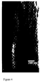
- Figure 4 shows a TEM micrograph layer of a thin layer (4 ⁇ m).
- S substrate
- P pumping unit
- M magnetron
- V s substrate potential (bias)
- I s substrate current
- V t target potential
- I t target current.
- a cutting tool for machining by chip removal of materials such as non-ferrous material such as aluminium alloys comprises a body of a hard alloy of cemented carbide, cermet, ceramics or high speed steel onto which a hard and wear resistant refractory coating is deposited.
- the wear resistant coating is composed of one or more layers of refractory compounds of which at least one layer, preferably the outermost layer, is composed of TiB 2 , and that the innermost layer(s), if any at all, between the tool body and the TiB 2 -layer, is composed of metal nitrides and/or carbides and/or oxides with the metal elements selected from Ti, Nb, Hf, V, Ta, Mo, Zr, Cr, W and Al.
- the TiB 2 -layers are a dense, crystalline TiB 2 free of cracks with a fine-grained fibrous morphology described below.
- the fine-grained fibrous TiB 2 -layer can also be deposited directly onto a cutting tool substrate of cemented carbide, cermet, ceramics or high speed steel.
- the thickness of the TiB 2 layer(s) varies from 0.5 to 60 ⁇ m preferably from 1 to 15 ⁇ m, for metal machining.
- the total coating thickness according to the present invention varies from 0.5 to 60 ⁇ m, preferably from 1 to 20 ⁇ m, with the thickness of the non-TiB 2 -layer(s) varying from 0.1 to 15 ⁇ m.
- layers of metal nitrides and/or carbides and/or oxide with the metal elements selected from Ti, Nb, Hf, V, Ta, Mo, Zr, Cr, W and Al can be deposited on top of the TiB 2 -layer.
- a process according to the present invention can be used to deposit layers thicker than 50 ⁇ m with retained mechanical properties and adhesion to the substrate, due to the capability of the process capability to grow layers free of intrinsic stress.
- thin layers (0.2 - 3 ⁇ m) with an increased effective adhesion can be deposited.
- the TiB 2 -layer is the outermost layer and with an average surface roughness R a of not more than 50 nm.
- This invention refers specially to a layer consisting of a fibrous morphology.
- PVD layers typically have a columnar morphology, i.e. - some grains have a tendency to increase in diameter on behalf of other grains.
- the TiB 2 layer according to present invention are grown in a mode where the fibrous morphology are kept almost unaffected from a layer thickness of 0.2 ⁇ m up to more than 60 ⁇ m. This morphology is in most cases preferable if a high cohesive strength of the grain boundaries are achieved. This is probably because of the small grain size in the direction of the abrasive wear, and large grain size in the direction of the applied compressive stress originating from the machining operation, giving a tougher coating material.
- Figure 1 shows a fracture cross-section of a relatively thin layer (4 ⁇ m) and Figure 2 shows a thick layer (60 ⁇ m). It is clearly evident that the morphology is almost unaffected by the layer thickness.
- Figure 4 shows a TEM micrograph layer of a thin layer (4 ⁇ m), that after the first fine grained nucleation zone, about 100 nm thick, the fibrous morphology develops.
- the cylindrical grains are typically 5-50 nm (in diameter), preferably 10-30 nm in average, ⁇ 15 nm in diameter, and a length more than 250 nm, preferably more than 400 nm.
- the fibrous grains have a length to diameter ratio, 1/d > 2, preferably > 5, and d varies little over the main length of the grains.
- the fibers are oriented essentially perpendicularly to the surface of the substrate.
- a texture coefficient, TC can be defined as.
- TiB 2 -layers according to the present invention exhibit a residual stress state of ⁇ tot ⁇ 0 GPa but larger than -1 GPa, preferably -0.5 GPa, when deposited on WC- 6 wt% Co substrate. This corresponds to an intrinsic stress state, ⁇ int , close to zero.
- ⁇ f and ⁇ sub the coefficient of thermal expansion of the film and substrate material.
- T dep and T ana the deposition and analyse temperature in K. It is important to do the estimate of the thermal stresses by using the thermal expansion in the a-direction of the TiB 2 lattice, since due to the (001) texture almost all grains are oriented so that direction is parallel to the substrate surface.
- ⁇ sub 4.8*10 -6
- ⁇ TiB2,a 3.56*10 -6
- E f 600 GPa
- ⁇ f 0.22
- T dep 773 K
- the residual stress, ⁇ tot is determined using the well-known beam deflection technique.
- TiB 2 layers with low compressive residual stresses are deposited by magnetron sputtering of a TiB 2 target under the following conditions:
- Layers deposited with the standard technology using negative V s have a columnar structure.
- columnar structure describes a layer morphology where the grains, after the initially nucleation zone, have conical shape some with increasing diameter (in the plane parallel to the substrate surface), and other grains with decreasing diameter. This mode of growth is controlled by competition between different grains, where some grow out from others.
- layers deposited with positive bias according to this invention consist of a fibrous morphology. No elements other than Ti, B, and small impurities of Ar are found in the layers, indicating that no sputtering from chamber walls occurs although the plasma potential probably is high when applying a positive potential.
- the low stress level of layers according to the present invention is due to a combination of three effects: first, increased bulk temperature and adatom mobility; secondly, minimisation of energetic ion bombardment during growth; and thirdly, an electron bombardment of the surface enhancing surface mobility and increasing the nucleation rates. Also, is it likely that the electron current increases the desorption rate of absorbed hydrogen and/or water molecules from the surface. All this together result in drastically reduced residual stress compared to layers grown with negative substrate bias.
- the residual stress state of layers grown according to present invention are almost free of intrinsic stress, i.e. - the slightly compressive stress state measured originate only from the difference in coefficient of thermal expansion between the substrate and the layer.
- the present invention has been described with reference to TiB 2 -layers. It is obvious that the method can also be applied to the deposition of other wear resistant material where high compressive stresses is a problem such as ZrB 2 -layers or other borides.
- TiB 2 -layers were deposited in a commercially available deposition system aimed for thin film deposition equipped with a dc magnetron sputter source with a TiB 2 target (12.5 ⁇ 25.5 cm 2 ).
- the substrates were cleaned in an ultrasonic bath of an alkali solution and in alcohol.
- the substrates were stationarily positioned 5 cm above the magnetron and resistively heated by an electron beam for 50 min to about 450°C.
- the substrates were argon-ion etched (ion current density 5.4 mA/cm 2 ) for 30 minutes using a substrate bias of -200V.
- the subsequent TiB 2 deposition was carried out at the following seven different bias voltages, V s ; -200V, -110V, +10V, +25V, +35V and +50V.
- the substrate current I s was +1.2 A for negative V s , irrespective of voltage.
- the substrate current changed sign from positive to negative.
- the current was also found to increase with increasing positive V s up to +25V whereafter it started to level of around 13 A for further V s increase.
- Ra The surface roughnesses, were measured with a interferometric method using a Wyco MD-2000 instrument.
- Ra of the coating be influenced by the surface roughness of the substrate for thin coatings, as in this example, here was Ra of the substrate ⁇ 5 nm. i.e. - the increase in Ra after deposition ( ⁇ 5 nm to ⁇ 20 nm) is extremely small.
- V s the substrate bias
- Cemented carbide cutting tool inserts, solid exchangeable end mill MM 16-20020-B120PF-M04 (WC-6 wt%Co) type were coated with a 30 ⁇ m thick layer of TiB 2 according to example 1 using a bias, V s , of +50 V.
- the coated milling cutters were tested versus an uncoated variant of the same tool, in a copying milling operation of graphite, at 4000-6000 rpm, feed 700 mm/min Variant Tool life, h Failure mode Uncoated 10 Flank wear, Vbmax 0.3 mm TiB 2 coated 40 Not end of tool life, Vbmax 0.1 mm
- Inserts coated with TiB 2 according to example 1 were tested. Coating of TiN (prior art) were compared with two different TiB 2 coated variants, deposited using V s of -110 V and +50 V, respectively. Also an uncoated variant was tested.
- the cemented carbide insert had a polished rake face prior to coating. The edge hone was sharp.
- the carbide had a composition of 6.0 wt-% Co, 0.5 wt-% TaC/NbC, balance WC.
- the coating of the insert consisted of TiN or TiB 2 with a total thickness of 3.0 -4.0 ⁇ m. Operation Square shoulder milling Work piece Plate Material AA7075 Insert type APEX160408FR-E08 Cutting speed 800 m/min Feed 0.2 mm/rev Depth of cut 6.0 - 10.0 mm Remarks dry milling
Landscapes
- Chemical & Material Sciences (AREA)
- Chemical Kinetics & Catalysis (AREA)
- Engineering & Computer Science (AREA)
- Materials Engineering (AREA)
- Mechanical Engineering (AREA)
- Metallurgy (AREA)
- Organic Chemistry (AREA)
- Physical Vapour Deposition (AREA)
- Cutting Tools, Boring Holders, And Turrets (AREA)
- Polishing Bodies And Polishing Tools (AREA)
Abstract
Description
- The present invention relates to a cutting tool for machining by chip removal comprising a substrate of cemented carbide, cermet, ceramics or high speed steel and a hard and wear resistant refractory coating. According to a preferred aspect, the coating is composed of one or more layers of refractory compounds of which at least one layer comprise a low compressive stress boride layer, e.g. TiB2 or ZrB2, preferably TiB2, deposited by Physical Vapour Deposition (PVD). The TiB2 and the rest of the layer(s), if any at all, are composed of metal nitrides and/or carbides and/or oxide with the metal elements chosen from Ti, Nb, Hf, V, Ta, Mo, Zr, Cr, W and Al.
- Industrial use of PVD TiB2 layers has so far been strongly limited due to the very high compressive stresses normally possessed by such layers. In recent years large efforts have been made to develop PVD processes for deposition of new ultra-hard thin layers, e.g. boron carbide (B4C), titanium diboride (TiB2) and cubic boron nitride (c-BN), for wear protection, especially of cutting tools. Although these layer materials are very attractive for the tooling industry, they have not yet become commercialised.
- The high hardness and Young's modulus of TiB2, as well as its chemical resistance, are attributed to the crystal structure and atomic bonding. In TiB2 the Ti atoms form a metallic hexagonal structure. In analogy with the usual notation ABABAB for hexagonal close packing, the stacking sequence of Ti in TiB2 will be AAA. The boron (B) atoms are situated interstitially between the A-layers forming a strong covalently bonded hexagonal net. The sequence may be described as AHAHAH where H denotes a boron layer. The combination of metallic Ti and strongly covalently bonded B results in a compound with high thermal and electrical conductivity as well as high yield strength and chemical resistance.
- TiB2 layers have been deposited by various PVD techniques, such as reactive sputtering, arc evaporation, and most commonly, magnetron sputtering. However, despite the very interesting properties of the TiB2 bulk material, these layers are generally of little commercial interest. Their stress level is too high, which limits the practical adhesion, and thereby the layer thickness. In addition, due to the high intrinsic stressed layers are too brittle and easily fail because of lack of cohesion.
- US 4,019,873 discloses a coated cemented carbide cutting tool insert. The coating is composed of two superimposed layers including an outer, extremely wear-resistant layer consisting essentially of aluminium oxide and/or zirconium oxide. The inner layer is composed of at least one boride selected from the group consisting of borides of the elements titanium, zirconium, hafnium, vanadium, niobium, tantalum, chromium, molybdenum and tungsten.
- US 4,268,582 discloses a coated cemented carbide cutting tool insert comprising a cemented carbide substrate, the surface regions thereof having diffused therein an element such as boron, silicon or aluminium. The inserts further comprise a layer disposed on the diffused substrate, the layer being a boride such as titanium boride, hafnium boride, zirconium boride or tantalum boride. In another embodiment, the coated cemented article further includes an interlayer sandwiched between the diffused substrate and the boride layer.
- Both these patents deposit the TiB2-layers by CVD. However, because of the high temperature during CVD-deposition undesirable cobaltboride-phases are formed. For that reason PVD deposition of TiB2-layers on WC-Co based substrates is preferred.
- M. Berger, M. Larsson and S. Hogmark, Surf. Coat. Technol., 124 (2000) 253-261 have grown TiB2 layers with magnetron sputtering using negative substrate bias varying from ―220V to ―50 V, the residual stress were very high (i.e. - compressive stress from ―10.2 GPa to ―7.9 GPa). Also, one variant using 0 V was grown also resulting in a very high compressive residual stress of -6.1 GPa. In this investigation no films were grown using positive bias.
- C. Mitterer, M. Rauter and P. Rödhammer, Surf. Coat. Technol., 41 (1990) 351-363 have grown TiB2 and Ti-B-N-C compound layers with magnetron sputtering using negative substrate bias. The TiB2 layers were in high compressive residual stresses (~-4 GPa).
- R. Wiedemann and H. Oettel, Surface Engineering, 14 4 (1998) 299-304 also have grown TiB2 layers using magnetron sputtering. A negative substrate bias was used resulting in intrinsic compressive stress of ~-2 GPa. The hardness was low (25-29 GPa).
- One possibility to obtain a low compressive residual stress state boride layer would be, for example, to grow at a high pressure, or other condition reducing ion bombardment. However, this will give a layer with a columnar structure, often associated with grain boundaries that lack density, and a cauliflower shaped surface morphology. This microstructure is not preferable since a typical application of TiB2 layers are, for example, machining of soft and sticky aluminium alloys, which require the coating of the cutting tool to have a very smooth top surface in order to reduce the tendency to form a build-up edge. Of course, grain boundaries that are not dense are detrimental for the wear-resistance of the coating.
- It is an object of the present invention to provide a TiB2-coated cemented carbide cutting tool insert.
- It is a further object of the present invention to provide a method for depositing TiB2 layers with low compressive residual stresses. The low stress TiB2 layer should possess a dense, fibrous microstructure, and a smooth top-surface.
- According to a first aspect, the present invention provides a cutting tool insert comprising a substrate and a coating, the coating comprising at least one layer of TiB2 having a fibrous microstructure wherein the (cylindrical) grains are 5-50 nm, an average of approximately 15 nm in diameter and more than 250 nm long, with a length to diameter ratio 1/d > 2, and the fibrous grains are oriented essentially perpendicularly to a surface of the substrate.
- According to a second aspect, the present invention provides a method of making a cutting tool insert comprising a substrate and a coating including at least one layer of TiB2 having a fibrous microstructure by PVD magnetron sputtering, the method compromising utilizing a bias voltage, Vs >0 V.
-
- Figure 1 is a photomicrograph of a cross-section of a relatively thin refractory layer formed according to the present invention.
- Figure 2 is a photomicrograph of a cross-section of a relatively thick refractory layer formed according to the present invention.
- Figure 3 is a schematic illustration of a magnetron sputtering device utilized in association with the present invention.
- Figure 4 is a TEM micrograph of a relatively thin layer formed according to the principles of the present invention.
-
- In the following description the residual stress state, σtot, denote the total stress of a coating on the actual substrate, i.e. - the sum of the thermal stresses, σthermal, due to difference in coefficient of thermal expansion between the substrate and the coating material, and the intrinsic stresses, σint, originating from the actual growth process, i.e. - σtot = σthermal + σint.
- Figure 1 shows the microstructure, in cross-section, of a relatively thin layer of TiB2-layer (4 µm), according to the present invention. Figure 2 is a corresponding picture of a thick layer (60 µm). Figure 3 schematically shows the used magnetron sputtering equipment. Figure 4 shows a TEM micrograph layer of a thin layer (4 µm).
- In these figures S = substrate, P = pumping unit, M = magnetron, sputtering source, Vs = substrate potential (bias), Is = substrate current, Vt = target potential, It = target current.
- According to the present invention there is provided a cutting tool for machining by chip removal of materials such as non-ferrous material such as aluminium alloys. The cutting tool comprises a body of a hard alloy of cemented carbide, cermet, ceramics or high speed steel onto which a hard and wear resistant refractory coating is deposited. The wear resistant coating is composed of one or more layers of refractory compounds of which at least one layer, preferably the outermost layer, is composed of TiB2, and that the innermost layer(s), if any at all, between the tool body and the TiB2-layer, is composed of metal nitrides and/or carbides and/or oxides with the metal elements selected from Ti, Nb, Hf, V, Ta, Mo, Zr, Cr, W and Al. The TiB2-layers are a dense, crystalline TiB2 free of cracks with a fine-grained fibrous morphology described below.
- The fine-grained fibrous TiB2-layer can also be deposited directly onto a cutting tool substrate of cemented carbide, cermet, ceramics or high speed steel. The thickness of the TiB2 layer(s) varies from 0.5 to 60 µm preferably from 1 to 15 µm, for metal machining. The total coating thickness according to the present invention varies from 0.5 to 60 µm, preferably from 1 to 20 µm, with the thickness of the non-TiB2-layer(s) varying from 0.1 to 15 µm. Further, layers of metal nitrides and/or carbides and/or oxide with the metal elements selected from Ti, Nb, Hf, V, Ta, Mo, Zr, Cr, W and Al can be deposited on top of the TiB2-layer.
- In an alternative embodiment, a process according to the present invention can be used to deposit layers thicker than 50 µm with retained mechanical properties and adhesion to the substrate, due to the capability of the process capability to grow layers free of intrinsic stress.
- In another alternative embodiment, thin layers (0.2 - 3 µm) with an increased effective adhesion can be deposited.
- In a preferred embodiment the TiB2-layer is the outermost layer and with an average surface roughness Ra of not more than 50 nm.
- This invention refers specially to a layer consisting of a fibrous morphology. PVD layers typically have a columnar morphology, i.e. - some grains have a tendency to increase in diameter on behalf of other grains. However, the TiB2 layer according to present invention are grown in a mode where the fibrous morphology are kept almost unaffected from a layer thickness of 0.2 µm up to more than 60 µm. This morphology is in most cases preferable if a high cohesive strength of the grain boundaries are achieved. This is probably because of the small grain size in the direction of the abrasive wear, and large grain size in the direction of the applied compressive stress originating from the machining operation, giving a tougher coating material. Figure 1 shows a fracture cross-section of a relatively thin layer (4 µm) and Figure 2 shows a thick layer (60 µm). It is clearly evident that the morphology is almost unaffected by the layer thickness. Figure 4 shows a TEM micrograph layer of a thin layer (4 µm), that after the first fine grained nucleation zone, about 100 nm thick, the fibrous morphology develops. The cylindrical grains are typically 5-50 nm (in diameter), preferably 10-30 nm in average, ~15 nm in diameter, and a length more than 250 nm, preferably more than 400 nm. The fibrous grains have a length to diameter ratio, 1/d > 2, preferably > 5, and d varies little over the main length of the grains. The fibers are oriented essentially perpendicularly to the surface of the substrate.
- The fine-grained, fibrous crystalline TiB2 according to the invention is strongly textured in the [001]-direction, a texture coefficient, TC, can be defined as.where

- I(hkl) = measured intensity of the (hkl) reflection
- Io(hkl) = standard intensity from the ASTM standard powder pattern diffraction data (JCPDS 35-0741)
- n = number of reflections used in the calculation (in this case 8)
- (hkl) reflections used are: (001), (100), (101), (110) (102 + 111), (201), (112) and (103 + 210). Where e.g. (103 + 210) means that those two, very close reflections, are treated as one reflection having the sum of intensity of the two. According to the present invention, the TC for the set of (001) crystal planes is greater than 5, preferably greater than 6.5.
-
- In addition, TiB2-layers according to the present invention exhibit a residual stress state of σtot <0 GPa but larger than -1 GPa, preferably -0.5 GPa, when deposited on WC- 6 wt% Co substrate. This corresponds to an intrinsic stress state, σint, close to zero. The thermal stresses, σthermal, can be calculated using
- The residual stress, σtot, is determined using the well-known beam deflection technique.
- The intrinsic stress can then be obtained by applying the equation:
- The intrinsic stress, σint, of coatings deposited with positive bias is therefore:
- According to the method of the present invention TiB2 layers with low compressive residual stresses are deposited by magnetron sputtering of a TiB2 target under the following conditions:
- Magnetron power: 3 -20 kW
- Substrate current Is: -1 - -15 A
- Atmosphere: Ar
- Pressure: <10-2 mbar, preferably <10-3 mbar
- Bias voltage Vs: >0 preferably > +5 V but < +60 V. The substrate current Is changes polarity because of the positive Vs. This corresponds to low energetic ion bombardment and electron bombardment of the growing layer surface.
-
- Layers deposited with the standard technology using negative Vs have a columnar structure. Here "columnar structure" describes a layer morphology where the grains, after the initially nucleation zone, have conical shape some with increasing diameter (in the plane parallel to the substrate surface), and other grains with decreasing diameter. This mode of growth is controlled by competition between different grains, where some grow out from others.
- On the other hand, layers deposited with positive bias according to this invention consist of a fibrous morphology. No elements other than Ti, B, and small impurities of Ar are found in the layers, indicating that no sputtering from chamber walls occurs although the plasma potential probably is high when applying a positive potential.
- While not intending to limit the invention to any particular theory, it is believed that the low stress level of layers according to the present invention is due to a combination of three effects: first, increased bulk temperature and adatom mobility; secondly, minimisation of energetic ion bombardment during growth; and thirdly, an electron bombardment of the surface enhancing surface mobility and increasing the nucleation rates. Also, is it likely that the electron current increases the desorption rate of absorbed hydrogen and/or water molecules from the surface. All this together result in drastically reduced residual stress compared to layers grown with negative substrate bias.
- The residual stress state of layers grown according to present invention are almost free of intrinsic stress, i.e. - the slightly compressive stress state measured originate only from the difference in coefficient of thermal expansion between the substrate and the layer.
- The present invention has been described with reference to TiB2-layers. It is obvious that the method can also be applied to the deposition of other wear resistant material where high compressive stresses is a problem such as ZrB2-layers or other borides.
- TiB2-layers were deposited in a commercially available deposition system aimed for thin film deposition equipped with a dc magnetron sputter source with a TiB2 target (12.5×25.5 cm2).
- Mirror-polished cemented carbide substrates with composition 6 wt% Co and 94 wt% WC were used. The WC grain size was about 1 µm and the hardness was 1650 HV10.
- Before deposition, the substrates were cleaned in an ultrasonic bath of an alkali solution and in alcohol. The substrates were stationarily positioned 5 cm above the magnetron and resistively heated by an electron beam for 50 min to about 450°C. Immediately after heating, the substrates were argon-ion etched (ion current density 5.4 mA/cm2) for 30 minutes using a substrate bias of -200V. The subsequent TiB2 deposition was carried out at the following seven different bias voltages, Vs; -200V, -110V, +10V, +25V, +35V and +50V. A magnetron power of 6 kW, resulting in a target potential of about 500V and an Ar pressure of 3x10⁻³ mbar were maintained during deposition of all layers. The resulting thickness of the positively biased layers was ~ 4 µm. The negatively biased layers were made somewhat thinner (~ 3 µm) to avoid layer failure due to their higher residual stresses. The substrate temperature was measured with a thermocouple attached to the substrate holder.
- The substrate current Is was +1.2 A for negative Vs, irrespective of voltage. When changing from negative to positive Vs the substrate current changed sign from positive to negative. The current was also found to increase with increasing positive Vs up to +25V whereafter it started to level of around 13 A for further Vs increase.
- Using a positive Vs resulted in a substrate temperature at the end of deposition Tdep increase to about 200°C higher than using negative Vs. However, the different positive or negative Vs did not significantly influence Tdep.
- XRD analysis showed that all films exhibited the hexagonal hcp-TiB2 phase with a strong (001) texture with a texture coefficient as defined above of 6.5 or more, i.e. - no other diffraction peaks where detected. The FWHM values of the (001) peak showed that the positively biased layers gave sharper peaks than those formed with negative Vs. No influence was seen on FWHM within the positive range of Vs, while for negative Vs, FHWM increased with the voltage.
- SEM studies of fracture cross-sections revealed columnar structure for layers deposited with negative Vs. It was more pronounced for ―200V than for ―110V. For positive Vs, no columnar growth was observed. However, in higher magnification, a dense, fibrous morphology was observed on positively biased layers see Figure 1. EDS analysis indicated that all layers were slightly overstoichiometric in B. The Ti/B ratio was typically 0.46 for all layers independent of Vs. Layers grown with negative Vs contained as much as 8 at% Ar for Vs = ―200V, while when using positive Vs no Ar could be detected. No other elements than Ti, B and Ar could be found in any layer.
- By applying a positive Vs, independent of value, layers with low compressive residual stress states, σtot ≈ ―0.5 GPa, were obtained. This stress state corresponds roughly to the thermal stress state. On the other hand, using negative Vs gave layers with residual stresses in the range of―7 to ―10 GPa.
- All layers exhibited H and E values of about 50 and 600 GPa (measured with nanoindentation technique), respectively.
- The abrasive wear rate was about 25-30 µm3/mmN for all layers, except the one grown with Vs = ―200V which showed about 50% higher wear rate than the other.
- From a scratch test it was concluded that the adhesion was good for all layers, and in all cases the initial layer failure was of a cohesive type. There was no significant difference in critical load FN,C among the layers deposited with positive bias. They were all in the 42-46 N range. The layers deposited with negative Vs displayed a lower FN,C, about 25-30 N, and also a higher amount of cohesive failures at the rim of the scratch, than layers deposited with positive Vs. Though, the scratch test demonstrate that coatings according to present invention have strongly enhanced toughness properties compared with coatings grown using negative bias.
- The surface roughnesses, Ra, were measured with a interferometric method using a Wyco MD-2000 instrument. Of course will Ra of the coating be influenced by the surface roughness of the substrate for thin coatings, as in this example, here was Ra of the substrate ~ 5 nm. i.e. - the increase in Ra after deposition (~5 nm to ~20 nm) is extremely small. It is obvious that the surface roughness decreases when changing the substrate bias, Vs, from negative to positive see table 1. However, no significant difference between different coatings grown with different positive bias could be seen.
Bias voltage and properties of the TiB2 layers. Vs [V] FWHM (001) [2] σ [GPa] H [GPa] E [GPa] FN,C [N] Wear rate [µm3/mmN] Ra [nm] Structure ―200V 0.495 10.5±0.8 50±5 605±70 29±1 61±7 75 Columnar ―110V 0.453 7.1±0.6 52±3 600±65 25±1 32±5 60 Columnar +10V 0.287 0.5±0.2 48±4 580±70 45±1 26±6 22 Fibrous +25V 0.304 0.3±0.2 49±7 560±95 43±1 36±8 18 Fibrous +35V 0.286 0.7±0.2 53±7 640±50 46±3 32±7 20 Fibrous +50V 0.290 0.5±0.2 54±9 600±85 42±1 25±3 15 Fibrous - Cemented carbide cutting tool inserts, solid exchangeable end mill MM 16-20020-B120PF-M04 (WC-6 wt%Co) type were coated with a 30 µm thick layer of TiB2 according to example 1 using a bias, Vs, of +50 V. The coated milling cutters were tested versus an uncoated variant of the same tool, in a copying milling operation of graphite, at 4000-6000 rpm, feed 700 mm/min
Variant Tool life, h Failure mode Uncoated 10 Flank wear, Vbmax 0.3 mm TiB2 coated 40 Not end of tool life, Vbmax 0.1 mm - Inserts coated with TiB2 according to example 1 were tested. Coating of TiN (prior art) were compared with two different TiB2 coated variants, deposited using Vs of -110 V and +50 V, respectively. Also an uncoated variant was tested. The cemented carbide insert had a polished rake face prior to coating. The edge hone was sharp. The carbide had a composition of 6.0 wt-% Co, 0.5 wt-% TaC/NbC, balance WC. The coating of the insert consisted of TiN or TiB2 with a total thickness of 3.0 -4.0 µm.
Operation Square shoulder milling Work piece Plate Material AA7075 Insert type APEX160408FR-E08 Cutting speed 800 m/min Feed 0.2 mm/rev Depth of cut 6.0 - 10.0 mm Remarks dry milling 
- A similar procedure to example 3 was utilized but using a lower cutting speed in order to promote build-up edge formation.
Operation Square shoulder milling Work piece Plate Material AA7075 Insert type APEX160408FR-E08 Cutting speed 650 m/min Feed 0.2 mm/rev Depth of cut 6.0 - 10.0 mm Remarks dry milling Variant Time at first formation of build-up edge (h) Degree of build-up edge Flank wear Vbmax (mm) Uncoated 0.5 Very Heavy 0.21 TiN Immediate Very Heavy 0.18 TiB2 (Vs = -110 V) 4.0 Heavy 0.08 TiB2 (Vs = +50 V) 6.5 Small Not measurable
Claims (7)
- A cutting tool insert comprising a substrate and a coating, the coating comprising at least one layer of TiB2 having a fibrous microstructure characterised in that the cylindrical grains are 5-50 nm in diameter, more than 250 nm long and with a length to diameter ratio 1/d > 2, and the fibrous grains are oriented essentially perpendicularly to a surface of the substrate.
- The cutting tool according to claim 1, characterised in that at least one TiB2-layer has a preferred growth orientation in the [001]-direction with a texture coefficient >5 defined as below:where
 I(hkl) = measured intensity of the (hkl) reflectionIo(hkl) = standard intensity from the ASTM standard powder pattern diffraction data (JCPDS 35-0741)n = number of reflections used in the calculation (in this case 8)(hkl) reflections used are: (001), (100), (101), (110) (102 + 111), (201), (112) and (103 + 210).
 - The cutting tool according to claim 1, characterised in that the TiB2-layer exhibits an intrinsic stress state, σint, close to zero, i.e. - between +0.5 GPa and ―1.0 GPa.
- The cutting tool according to claim 1, characterised in that the TiB2 layer is the outermost layer and has an average surface roughness Ra not more than 50 nm.
- The cutting tool according to claim 1, characterised in that the cylindrical grains are 10-30 nm in diameter, more than 400 nm long and with a length to diameter ratio 1/d > 5.
- A method of making a cutting tool insert comprising a substrate and a coating including at least one layer of TiB2 having a fibrous microstructure by PVD magnetron sputtering, characterised in the method comprising the use of a bias voltage, Vs >0 V.
- The method of claim 6, characterised in that the bias voltage is + 5V to +60V.
Applications Claiming Priority (2)
| Application Number | Priority Date | Filing Date | Title |
|---|---|---|---|
| SE0101111 | 2001-03-28 | ||
| SE0101111A SE522722C2 (en) | 2001-03-28 | 2001-03-28 | Cutting tool coated with titanium diboride |
Publications (2)
| Publication Number | Publication Date |
|---|---|
| EP1245693A1 true EP1245693A1 (en) | 2002-10-02 |
| EP1245693B1 EP1245693B1 (en) | 2010-10-27 |
Family
ID=20283582
Family Applications (1)
| Application Number | Title | Priority Date | Filing Date |
|---|---|---|---|
| EP02445042A Expired - Lifetime EP1245693B1 (en) | 2001-03-28 | 2002-03-26 | Coated cutting tool |
Country Status (6)
| Country | Link |
|---|---|
| US (2) | US6770358B2 (en) |
| EP (1) | EP1245693B1 (en) |
| JP (1) | JP4184691B2 (en) |
| AT (1) | ATE486153T1 (en) |
| DE (1) | DE60238092D1 (en) |
| SE (1) | SE522722C2 (en) |
Cited By (3)
| Publication number | Priority date | Publication date | Assignee | Title |
|---|---|---|---|---|
| CN102528105A (en) * | 2010-11-25 | 2012-07-04 | 三菱综合材料株式会社 | Surface coating cutting tool |
| WO2018140990A1 (en) * | 2017-01-31 | 2018-08-09 | Ceratizit Austria Gesellschaft M.B.H. | Coated tool |
| EP3865233A4 (en) * | 2018-10-10 | 2022-03-23 | Sumitomo Electric Hardmetal Corp. | Cutting tool and manufacturing method therefor |
Families Citing this family (29)
| Publication number | Priority date | Publication date | Assignee | Title |
|---|---|---|---|---|
| US7660705B1 (en) | 2002-03-19 | 2010-02-09 | Microsoft Corporation | Bayesian approach for learning regression decision graph models and regression models for time series analysis |
| CA2502575A1 (en) * | 2002-11-15 | 2004-06-03 | University Of Utah Research Foundation | Integral titanium boride coatings on titanium surfaces and associated methods |
| US7580813B2 (en) * | 2003-06-17 | 2009-08-25 | Microsoft Corporation | Systems and methods for new time series model probabilistic ARMA |
| JP2006022368A (en) * | 2004-07-07 | 2006-01-26 | Shinko Seiki Co Ltd | Surface treating apparatus and surface treating method |
| US7596475B2 (en) * | 2004-12-06 | 2009-09-29 | Microsoft Corporation | Efficient gradient computation for conditional Gaussian graphical models |
| US7421380B2 (en) * | 2004-12-14 | 2008-09-02 | Microsoft Corporation | Gradient learning for probabilistic ARMA time-series models |
| US7459105B2 (en) * | 2005-05-10 | 2008-12-02 | University Of Utah Research Foundation | Nanostructured titanium monoboride monolithic material and associated methods |
| US7617010B2 (en) * | 2005-12-28 | 2009-11-10 | Microsoft Corporation | Detecting instabilities in time series forecasting |
| JP2008238281A (en) * | 2007-03-26 | 2008-10-09 | Hitachi Tool Engineering Ltd | Coated tool |
| US8388709B2 (en) * | 2007-12-06 | 2013-03-05 | Ceratizit Austria Gesellschaft GmbH | Coated article |
| US8845867B2 (en) * | 2008-12-09 | 2014-09-30 | Tdk Corporation | Method for manufacturing magnetoresistance effect element using simultaneous sputtering of Zn and ZnO |
| US20100176339A1 (en) * | 2009-01-12 | 2010-07-15 | Chandran K S Ravi | Jewelry having titanium boride compounds and methods of making the same |
| JP5402516B2 (en) * | 2009-10-19 | 2014-01-29 | 三菱マテリアル株式会社 | Surface coated cutting tool with excellent chipping resistance due to hard coating layer |
| EP2369031B1 (en) * | 2010-03-18 | 2016-05-04 | Oerlikon Trading AG, Trübbach | Coating on a nial2o4 basis in spinel structure |
| JP5488824B2 (en) * | 2010-08-12 | 2014-05-14 | 三菱マテリアル株式会社 | Surface-coated cutting tool that exhibits excellent peeling resistance and excellent wear resistance due to high-speed cutting of hard difficult-to-cut materials |
| KR101544659B1 (en) * | 2011-02-01 | 2015-08-17 | 오에스지 가부시키가이샤 | Hard multilayer coating film |
| WO2012105002A1 (en) * | 2011-02-01 | 2012-08-09 | オーエスジー株式会社 | Hard laminated coating |
| KR101544661B1 (en) * | 2011-02-01 | 2015-08-17 | 오에스지 가부시키가이샤 | Hard laminated coating |
| US9340863B2 (en) | 2011-12-15 | 2016-05-17 | Kobe Steel, Ltd. | Multilayer hard film and method for producing same |
| US9381575B2 (en) * | 2012-02-27 | 2016-07-05 | Sumitomo Electric Hardmetal Corp. | Surface-coated cutting tool and method of manufacturing the same |
| JP6213867B2 (en) * | 2013-02-21 | 2017-10-18 | 住友電工ハードメタル株式会社 | Surface-coated cutting tool and manufacturing method thereof |
| DE102013011075A1 (en) * | 2013-07-03 | 2015-01-08 | Oerlikon Trading Ag | TiB2 layers and their preparation |
| WO2016015771A1 (en) * | 2014-07-31 | 2016-02-04 | Bic-Violex Sa | Razor blade coating |
| RU2685820C1 (en) * | 2018-04-18 | 2019-04-23 | Общество с ограниченной ответственностью "Сборные конструкции инструмента, фрезы Москвитина" | Cutting tool with wear-resistant coating |
| WO2020075356A1 (en) * | 2018-10-10 | 2020-04-16 | 住友電工ハードメタル株式会社 | Cutting tool and manufacturing method therefor |
| CN112063983B (en) * | 2020-07-31 | 2021-11-05 | 广东工业大学 | Belt HfB2Coated cutting tool and method for producing the same |
| AT17511U1 (en) * | 2020-12-15 | 2022-06-15 | Plansee Se | TITANIUM-IBORIDE COATED REFRACTORY METAL COMPONENT |
| CN115612984A (en) * | 2022-09-09 | 2023-01-17 | 中国科学院金属研究所 | Titanium diboride coating with stress and structural gradient and preparation method thereof |
| CN117921043A (en) * | 2024-03-22 | 2024-04-26 | 赣州澳克泰工具技术有限公司 | CVD (chemical vapor deposition) coating cutter and preparation method thereof |
Family Cites Families (13)
| Publication number | Priority date | Publication date | Assignee | Title |
|---|---|---|---|---|
| DE2525185C3 (en) | 1975-06-06 | 1986-04-17 | Fried. Krupp Gmbh, 4300 Essen | Hard metal body |
| US4268582A (en) | 1979-03-02 | 1981-05-19 | General Electric Company | Boride coated cemented carbide |
| US4343865A (en) * | 1981-06-24 | 1982-08-10 | General Electric Company | Hard metal body and method of making same |
| US4761346A (en) * | 1984-11-19 | 1988-08-02 | Avco Corporation | Erosion-resistant coating system |
| DE3512986A1 (en) * | 1985-04-11 | 1986-10-16 | Kernforschungszentrum Karlsruhe Gmbh, 7500 Karlsruhe | VIELLAGE, HIGH-WEAR-RESISTANT HARD MATERIAL PROTECTIVE LAYER FOR METALLIC, STRICTLY STRESSED SURFACES OR SUBSTRATES |
| US4692385A (en) * | 1986-04-14 | 1987-09-08 | Materials Development Corporation | Triplex article |
| JPS6428358A (en) * | 1987-07-22 | 1989-01-30 | Kobe Steel Ltd | Hard coated member |
| US4820392A (en) * | 1987-12-21 | 1989-04-11 | Ford Motor Company | Method of increasing useful life of tool steel cutting tools |
| US5453168A (en) * | 1993-08-25 | 1995-09-26 | Tulip Memory Systems, Inc. | Method for forming protective overcoatings for metallic-film magnetic-recording mediums |
| US5952085A (en) * | 1994-03-23 | 1999-09-14 | Rolls-Royce Plc | Multiple layer erosion resistant coating and a method for its production |
| DE59406283D1 (en) * | 1994-08-17 | 1998-07-23 | Asea Brown Boveri | Process for producing a turbine blade made of an (alpha-beta) titanium-based alloy |
| US5945214C1 (en) * | 1996-08-28 | 2002-04-23 | Premark Rwp Holdings Inc | Diboride coated pressing surfaces for abrasion resistant laminate and making pressing surfaces |
| US6287711B1 (en) * | 1998-07-01 | 2001-09-11 | Front Edge Technology, Inc. | Wear-resistant coating and component |
-
2001
- 2001-03-28 SE SE0101111A patent/SE522722C2/en not_active IP Right Cessation
-
2002
- 2002-03-26 EP EP02445042A patent/EP1245693B1/en not_active Expired - Lifetime
- 2002-03-26 DE DE60238092T patent/DE60238092D1/en not_active Expired - Lifetime
- 2002-03-26 AT AT02445042T patent/ATE486153T1/en active
- 2002-03-27 US US10/106,116 patent/US6770358B2/en not_active Expired - Fee Related
- 2002-03-28 JP JP2002092667A patent/JP4184691B2/en not_active Expired - Fee Related
-
2004
- 2004-05-19 US US10/848,012 patent/US6939445B2/en not_active Expired - Fee Related
Non-Patent Citations (3)
| Title |
|---|
| BERGER A ET AL: "Low stress TiB/sub 2/ coatings with improved tribological properties", THIN SOLID FILMS, 17 DEC. 2001, ELSEVIER, SWITZERLAND, vol. 401, no. 1-2, pages 179 - 186, XP004312805, ISSN: 0040-6090 * |
| BERGER M ET AL: "Evaluation of magnetron-sputtered TiB/sub 2/ intended for tribological applications", SURFACE AND COATINGS TECHNOLOGY, 21 FEB. 2000, ELSEVIER, SWITZERLAND, vol. 124, no. 2-3, pages 253 - 261, XP002205675, ISSN: 0257-8972 * |
| LOSBICHLER P ET AL: "Non-reactively sputtered TiN and TiB/sub 2/ films: influence of activation energy on film growth", FIFTH INTERNATIONAL CONFERENCE ON PLASMA SURFACE ENGINEERING, GARMISCH-PARTENKIRCHEN, GERMANY, 9-13 SEPT. 1996, vol. 97, no. 1-3, Surface and Coatings Technology, Dec. 1997, Elsevier, Switzerland, pages 567 - 573, XP002205676, ISSN: 0257-8972 * |
Cited By (4)
| Publication number | Priority date | Publication date | Assignee | Title |
|---|---|---|---|---|
| CN102528105A (en) * | 2010-11-25 | 2012-07-04 | 三菱综合材料株式会社 | Surface coating cutting tool |
| WO2018140990A1 (en) * | 2017-01-31 | 2018-08-09 | Ceratizit Austria Gesellschaft M.B.H. | Coated tool |
| US11104999B2 (en) | 2017-01-31 | 2021-08-31 | Ceratizit Austria Gesellschaft M.B.H. | Coated tool |
| EP3865233A4 (en) * | 2018-10-10 | 2022-03-23 | Sumitomo Electric Hardmetal Corp. | Cutting tool and manufacturing method therefor |
Also Published As
| Publication number | Publication date |
|---|---|
| JP4184691B2 (en) | 2008-11-19 |
| US6939445B2 (en) | 2005-09-06 |
| US6770358B2 (en) | 2004-08-03 |
| SE0101111L (en) | 2002-09-29 |
| JP2002355704A (en) | 2002-12-10 |
| US20040214033A1 (en) | 2004-10-28 |
| US20030039867A1 (en) | 2003-02-27 |
| DE60238092D1 (en) | 2010-12-09 |
| SE0101111D0 (en) | 2001-03-28 |
| SE522722C2 (en) | 2004-03-02 |
| EP1245693B1 (en) | 2010-10-27 |
| ATE486153T1 (en) | 2010-11-15 |
Similar Documents
| Publication | Publication Date | Title |
|---|---|---|
| EP1245693B1 (en) | Coated cutting tool | |
| KR100614961B1 (en) | PVD Al2 O3 COATED CUTTING TOOL | |
| EP0701982B1 (en) | Layered film made of ultrafine particles and a hard composite material for tools possessing the film | |
| PalDey et al. | Single layer and multilayer wear resistant coatings of (Ti, Al) N: a review | |
| US7067203B2 (en) | Wear resistant coating with enhanced toughness | |
| US7083868B2 (en) | Composite structured wear resistant coating | |
| EP0983393B1 (en) | Multilayered coated cutting tool | |
| JP6687390B2 (en) | Tool with TiAlCrSiN coating by PVD | |
| EP1932947B1 (en) | Coated cutting tool | |
| EP2141257B1 (en) | Oxide coated cutting insert and cathodic arc deposition associated | |
| US20020051852A1 (en) | PVD coated cutting tool and method of its production | |
| CA2789838A1 (en) | Multilayer coated wear-resistant member and method for making the same | |
| KR101590203B1 (en) | Oxide coated cutting insert | |
| EP2262925A1 (en) | Oxide coated cutting insert | |
| WO2021122892A1 (en) | A coated cutting tool | |
| JP2001517156A (en) | Multi-layer coated cutting tool | |
| Buttler | 10.8 Surface hardening and hard coatings | |
| JPH08318407A (en) | Covering cutting tool | |
| CN117737648A (en) | Method for producing a coated body and coated body obtainable according to said method | |
| Ducros et al. | Multilayered and nanolayered hard nitride thin films for a better yield in micro machining. |
Legal Events
| Date | Code | Title | Description |
|---|---|---|---|
| PUAI | Public reference made under article 153(3) epc to a published international application that has entered the european phase |
Free format text: ORIGINAL CODE: 0009012 |
|
| AK | Designated contracting states |
Kind code of ref document: A1 Designated state(s): AT BE CH CY DE DK ES FI FR GB GR IE IT LI LU MC NL PT SE TR |
|
| AX | Request for extension of the european patent |
Free format text: AL;LT;LV;MK;RO;SI |
|
| 17P | Request for examination filed |
Effective date: 20030328 |
|
| AKX | Designation fees paid |
Designated state(s): AT BE CH CY DE DK ES FI FR GB GR IE IT LI LU MC NL PT SE TR |
|
| GRAP | Despatch of communication of intention to grant a patent |
Free format text: ORIGINAL CODE: EPIDOSNIGR1 |
|
| GRAS | Grant fee paid |
Free format text: ORIGINAL CODE: EPIDOSNIGR3 |
|
| RAP1 | Party data changed (applicant data changed or rights of an application transferred) |
Owner name: SECO TOOLS AB |
|
| GRAA | (expected) grant |
Free format text: ORIGINAL CODE: 0009210 |
|
| RAP1 | Party data changed (applicant data changed or rights of an application transferred) |
Owner name: SECO TOOLS AB |
|
| AK | Designated contracting states |
Kind code of ref document: B1 Designated state(s): AT BE CH CY DE DK ES FI FR GB GR IE IT LI LU MC NL PT SE TR |
|
| REG | Reference to a national code |
Ref country code: GB Ref legal event code: FG4D |
|
| REG | Reference to a national code |
Ref country code: CH Ref legal event code: PCOW Free format text: SECO TOOLS AB; ;737 82 FAGERSTA (SE) Ref country code: CH Ref legal event code: NV Representative=s name: BOVARD AG PATENTANWAELTE Ref country code: CH Ref legal event code: EP |
|
| REG | Reference to a national code |
Ref country code: IE Ref legal event code: FG4D |
|
| REF | Corresponds to: |
Ref document number: 60238092 Country of ref document: DE Date of ref document: 20101209 Kind code of ref document: P |
|
| REG | Reference to a national code |
Ref country code: SE Ref legal event code: TRGR |
|
| REG | Reference to a national code |
Ref country code: NL Ref legal event code: VDEP Effective date: 20101027 |
|
| REG | Reference to a national code |
Ref country code: CH Ref legal event code: PFA Owner name: SECO TOOLS AB Free format text: SECO TOOLS AB# #737 82 FAGERSTA (SE) -TRANSFER TO- SECO TOOLS AB# #737 82 FAGERSTA (SE) |
|
| PG25 | Lapsed in a contracting state [announced via postgrant information from national office to epo] |
Ref country code: PT Free format text: LAPSE BECAUSE OF FAILURE TO SUBMIT A TRANSLATION OF THE DESCRIPTION OR TO PAY THE FEE WITHIN THE PRESCRIBED TIME-LIMIT Effective date: 20110228 Ref country code: NL Free format text: LAPSE BECAUSE OF FAILURE TO SUBMIT A TRANSLATION OF THE DESCRIPTION OR TO PAY THE FEE WITHIN THE PRESCRIBED TIME-LIMIT Effective date: 20101027 Ref country code: FI Free format text: LAPSE BECAUSE OF FAILURE TO SUBMIT A TRANSLATION OF THE DESCRIPTION OR TO PAY THE FEE WITHIN THE PRESCRIBED TIME-LIMIT Effective date: 20101027 |
|
| PG25 | Lapsed in a contracting state [announced via postgrant information from national office to epo] |
Ref country code: BE Free format text: LAPSE BECAUSE OF FAILURE TO SUBMIT A TRANSLATION OF THE DESCRIPTION OR TO PAY THE FEE WITHIN THE PRESCRIBED TIME-LIMIT Effective date: 20101027 Ref country code: GR Free format text: LAPSE BECAUSE OF FAILURE TO SUBMIT A TRANSLATION OF THE DESCRIPTION OR TO PAY THE FEE WITHIN THE PRESCRIBED TIME-LIMIT Effective date: 20110128 |
|
| PG25 | Lapsed in a contracting state [announced via postgrant information from national office to epo] |
Ref country code: ES Free format text: LAPSE BECAUSE OF FAILURE TO SUBMIT A TRANSLATION OF THE DESCRIPTION OR TO PAY THE FEE WITHIN THE PRESCRIBED TIME-LIMIT Effective date: 20110207 |
|
| PG25 | Lapsed in a contracting state [announced via postgrant information from national office to epo] |
Ref country code: DK Free format text: LAPSE BECAUSE OF FAILURE TO SUBMIT A TRANSLATION OF THE DESCRIPTION OR TO PAY THE FEE WITHIN THE PRESCRIBED TIME-LIMIT Effective date: 20101027 |
|
| PLBE | No opposition filed within time limit |
Free format text: ORIGINAL CODE: 0009261 |
|
| STAA | Information on the status of an ep patent application or granted ep patent |
Free format text: STATUS: NO OPPOSITION FILED WITHIN TIME LIMIT |
|
| 26N | No opposition filed |
Effective date: 20110728 |
|
| PG25 | Lapsed in a contracting state [announced via postgrant information from national office to epo] |
Ref country code: MC Free format text: LAPSE BECAUSE OF NON-PAYMENT OF DUE FEES Effective date: 20110331 |
|
| REG | Reference to a national code |
Ref country code: DE Ref legal event code: R097 Ref document number: 60238092 Country of ref document: DE Effective date: 20110728 |
|
| REG | Reference to a national code |
Ref country code: IE Ref legal event code: MM4A |
|
| PG25 | Lapsed in a contracting state [announced via postgrant information from national office to epo] |
Ref country code: IE Free format text: LAPSE BECAUSE OF NON-PAYMENT OF DUE FEES Effective date: 20110326 |
|
| PGFP | Annual fee paid to national office [announced via postgrant information from national office to epo] |
Ref country code: FR Payment date: 20120319 Year of fee payment: 11 Ref country code: CH Payment date: 20120313 Year of fee payment: 11 |
|
| PGFP | Annual fee paid to national office [announced via postgrant information from national office to epo] |
Ref country code: SE Payment date: 20120313 Year of fee payment: 11 Ref country code: IT Payment date: 20120320 Year of fee payment: 11 Ref country code: GB Payment date: 20120321 Year of fee payment: 11 |
|
| PGFP | Annual fee paid to national office [announced via postgrant information from national office to epo] |
Ref country code: DE Payment date: 20120411 Year of fee payment: 11 |
|
| PGFP | Annual fee paid to national office [announced via postgrant information from national office to epo] |
Ref country code: AT Payment date: 20120228 Year of fee payment: 11 |
|
| PG25 | Lapsed in a contracting state [announced via postgrant information from national office to epo] |
Ref country code: CY Free format text: LAPSE BECAUSE OF FAILURE TO SUBMIT A TRANSLATION OF THE DESCRIPTION OR TO PAY THE FEE WITHIN THE PRESCRIBED TIME-LIMIT Effective date: 20101027 Ref country code: LU Free format text: LAPSE BECAUSE OF NON-PAYMENT OF DUE FEES Effective date: 20110326 |
|
| PG25 | Lapsed in a contracting state [announced via postgrant information from national office to epo] |
Ref country code: TR Free format text: LAPSE BECAUSE OF FAILURE TO SUBMIT A TRANSLATION OF THE DESCRIPTION OR TO PAY THE FEE WITHIN THE PRESCRIBED TIME-LIMIT Effective date: 20101027 |
|
| REG | Reference to a national code |
Ref country code: SE Ref legal event code: EUG |
|
| PG25 | Lapsed in a contracting state [announced via postgrant information from national office to epo] |
Ref country code: SE Free format text: LAPSE BECAUSE OF NON-PAYMENT OF DUE FEES Effective date: 20130327 |
|
| REG | Reference to a national code |
Ref country code: CH Ref legal event code: PL |
|
| REG | Reference to a national code |
Ref country code: AT Ref legal event code: MM01 Ref document number: 486153 Country of ref document: AT Kind code of ref document: T Effective date: 20130326 |
|
| GBPC | Gb: european patent ceased through non-payment of renewal fee |
Effective date: 20130326 |
|
| REG | Reference to a national code |
Ref country code: FR Ref legal event code: ST Effective date: 20131129 |
|
| REG | Reference to a national code |
Ref country code: DE Ref legal event code: R119 Ref document number: 60238092 Country of ref document: DE Effective date: 20131001 |
|
| PG25 | Lapsed in a contracting state [announced via postgrant information from national office to epo] |
Ref country code: DE Free format text: LAPSE BECAUSE OF NON-PAYMENT OF DUE FEES Effective date: 20131001 Ref country code: LI Free format text: LAPSE BECAUSE OF NON-PAYMENT OF DUE FEES Effective date: 20130331 Ref country code: CH Free format text: LAPSE BECAUSE OF NON-PAYMENT OF DUE FEES Effective date: 20130331 Ref country code: GB Free format text: LAPSE BECAUSE OF NON-PAYMENT OF DUE FEES Effective date: 20130326 Ref country code: FR Free format text: LAPSE BECAUSE OF NON-PAYMENT OF DUE FEES Effective date: 20130402 Ref country code: AT Free format text: LAPSE BECAUSE OF NON-PAYMENT OF DUE FEES Effective date: 20130326 |
|
| PG25 | Lapsed in a contracting state [announced via postgrant information from national office to epo] |
Ref country code: IT Free format text: LAPSE BECAUSE OF NON-PAYMENT OF DUE FEES Effective date: 20130326 |