EP1244219A2 - Method and apparatus for digital-to-analog conversion with an effective pulse width modulation - Google Patents
Method and apparatus for digital-to-analog conversion with an effective pulse width modulation Download PDFInfo
- Publication number
- EP1244219A2 EP1244219A2 EP02006572A EP02006572A EP1244219A2 EP 1244219 A2 EP1244219 A2 EP 1244219A2 EP 02006572 A EP02006572 A EP 02006572A EP 02006572 A EP02006572 A EP 02006572A EP 1244219 A2 EP1244219 A2 EP 1244219A2
- Authority
- EP
- European Patent Office
- Prior art keywords
- bits
- pulse
- width
- digital data
- bit digital
- Prior art date
- Legal status (The legal status is an assumption and is not a legal conclusion. Google has not performed a legal analysis and makes no representation as to the accuracy of the status listed.)
- Granted
Links
Images









Classifications
-
- G—PHYSICS
- G06—COMPUTING OR CALCULATING; COUNTING
- G06F—ELECTRIC DIGITAL DATA PROCESSING
- G06F1/00—Details not covered by groups G06F3/00 - G06F13/00 and G06F21/00
- G06F1/02—Digital function generators
- G06F1/025—Digital function generators for functions having two-valued amplitude, e.g. Walsh functions
-
- H—ELECTRICITY
- H03—ELECTRONIC CIRCUITRY
- H03M—CODING; DECODING; CODE CONVERSION IN GENERAL
- H03M1/00—Analogue/digital conversion; Digital/analogue conversion
- H03M1/66—Digital/analogue converters
- H03M1/68—Digital/analogue converters with conversions of different sensitivity, i.e. one conversion relating to the more significant digital bits and another conversion to the less significant bits
-
- H—ELECTRICITY
- H03—ELECTRONIC CIRCUITRY
- H03M—CODING; DECODING; CODE CONVERSION IN GENERAL
- H03M1/00—Analogue/digital conversion; Digital/analogue conversion
- H03M1/66—Digital/analogue converters
- H03M1/82—Digital/analogue converters with intermediate conversion to time interval
- H03M1/822—Digital/analogue converters with intermediate conversion to time interval using pulse width modulation
Definitions
- the present invention relates to a method and apparatus for digital-to-analog conversion, and more particularly to a method and apparatus for digital-to-analog conversion with an effective pulse width modulation.
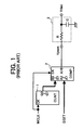
- Fig. 1 shows a typical structure of a digital-to-analog converter according to the prior art that converts digital data into analog data with a pulse width modulation (PWM) technique which is described, for example, in Japanese unexamined utility publications, No. 3-53042 (1991) and No. 6-13231 (1992).
- PWM pulse width modulation
- the digital-to-analog converter (often referred to as a DA converter or a DAC) of the prior art includes a ring counter (COUNT) 1, a magnitude comparator (COMP) 2, and an RC circuit 3.
- the ring counter 1 counts inputs of a main clock signal MCLK and outputs clock count information composed of eight bits, for example, which bit number is equivalent to a resolution of the DAC. That is, the resolution of the DAC is 1/256 in this case.
- a cycle of the main clock MCLK is referred to as Tmclk and an eight-bit counting cycle of the ring counter 1 is referred to as a pulse width modulation cycle Tpwm.
- the cycle Tpwm is composed of 256 Tmclk.
- the magnitude comparator 2 receives the eight-bit clock count information in input terminals B0 - B7 and a data set DSET composed of eight bits, which number of bits is equal to that of the clock count information, in input terminals A0 - A7.
- the eight-bit data set DSET has a value corresponding to a desired output level and is sent from a CPU (central processing unit) or the like (not shown).
- the DA converter of the prior art is a converter used, for example, for a feed back circuit for adjusting a direct current level of an analog signal or a full-scale or zero-scale level of an analog-to-digital (AD) converter in a control for automatically adjusting a reading level of a reading mechanism in a digital copying machine, a scanner, or the like.
- the data set DSET applied to this DA converter is changed in a cycle sufficiently longer than the pulse width modulation cycle Tpwm.
- the ring counter 1 counts the main clock MCLK all the time and outputs a count value with the eight-bit output terminals Q0 - Q7 to the input terminals B0 - B7 of the magnitude comparator 2.
- the comparator 2 compares the count value with the value of the data set DSET. During the time the count value is smaller than the data set DSET, the comparator 2 outputs a pulse signal Vpwm in a high state which has a pulse width corresponding to the value of the data set DSET, as shown in Fig. 2.
- the pulse signal Vpwm is smoothed through the RC circuit 3 composed of a resister R and a capacitor C and a resultant analog voltage Vdac in response to the value of the data set DSET is output.
- letters Th represent a time length of the pulse signal Vpwm in a high state which is composed of Tmclk multiplied by the value of the data set DSET.
- Letters Tl represent a time length of the pulse signal Vpwm in a low state which is composed of Tmclk multiplied by a value of 256 Tmclk subtracted by the data set DSET.
- Fig. 3 is a time chart showing a relationship between the pulse signal Vpwm and the analog voltage Vdac in two exemplary cases at the same time.
- the value of the data set DSET is set to 128, for example, and the related signal and waveform are labeled with a suffix numeral 128.
- the value of the data set DSET is set to 64, for example, and the related signal and waveform are labeled with a suffix numeral 64.
- Vpwm128 indicates as the pulse signal Vpwm in the case where the data set DSET is set to 128 and Vpwm64 indicates as the pulse signal Vpwm in the case where the data set DSET is set to 64.
- a mean voltage of the analog voltage Vdac128 is referred to as Vdacm128 and a mean value of the analog voltage Vdac64 is referred to as Vdacm64.
- Vdac (DSET/256)x(Vh-Vl) + Vl, wherein Vh represents the pulse signal Vpwm in a high state and Vl represents the pulse signal Vpwm in a low state.
- an amount of change in the analog voltage Vdac during the time the pulse signal Vpwm in a high state or a low state should necessarily be smaller than a half the resolution of the DAC.
- an amount of change in the analog voltage Vdac should satisfy the following relationships (1) and (2):
- the present application provides a novel digital-to-analog converter and a novel method of digital-to-analog conversion for converting n-bit digital data to an analog voltage according to any of the appended claims. Further advantageous embodiments are the subject-matter of the dependent claims.
- This patent specification describes a novel digital-to-analog converter for converting n-bit digital data to an analog voltage, wherein n is an arbitrary integer and the n bits are composed of upper nh bits and lower nl bits.
- this novel digital-to-analog converter includes a signal generator, a low-weighted value manager, and a voltage smoothing circuit.
- the signal generator is arranged and configured to perform a pulse width modulation based on inputs of a reference clock signal and the upper nh bits of the n-bit digital data and to generate a first pulse-width-modulated signal having a plurality of first pulses having a first pulse width in response to a value of the upper nh bits of the n-bit digital data and a pwm cycle signal indicating a cycle of a pulse width modulation performed.
- the low-weighted value manager is arranged and configured to receive the pulse-width-modulated signal, the pwm cycle signal, and the lower nl bits of the n-bit digital data, to divide a pulse width in response to a value of the lower nl bits of the n-bit digital data into a plurality of fraction pulse widths, to respectively add the plurality of fraction pulse widths to the plurality of first pulses, and to generate a second pulse-width-modulated signal having a plurality of second pulses having the first pulse width and one of the plurality of fraction pulse widths.
- the voltage smoothing circuit is arranged and configured to smooth the second pulse-width-modulated signal.
- This patent specification further describes a novel digital-to-analog converter for converting n-bit digital data to an analog voltage, wherein n is an arbitrary integer and the n bits are composed of upper nh bits and lower nl bits.
- this novel digital-to-analog converter includes a signal generator, an amplitude regulator, a bottom-level regulator, a voltage adding circuit, and a voltage smoothing circuit.
- the signal generator is arranged and configured to perform a pulse width modulation based on inputs of a reference clock signal and the lower nl bits of the n-bit digital data and to generate a pulse-width-modulated signal having a plurality of first pulses having a first pulse width in response to a value of the lower nh bits of the n-bit digital data.
- the amplitude regulator is arranged and configured to regulate an amplitude of the pulse-width-modulated signal generated by the signal generator.
- the bottom-level regulator is arranged and configured to receive the upper nh bits of the n-bit digital data and to regulate a bottom level of a voltage in accordance with a value of the upper nh bits of the n-bits digital data.
- the voltage adding circuit is arranged and configured to add the pulse-width-modulated signal having an amplitude regulated by the amplitude regulator to the voltage having a bottom level regulated by the bottom-level regulator and to output a composite voltage.
- the voltage smoothing circuit is arranged and configured to smooth the composite voltage output by the voltage adding circuit.
- This patent specification further descrbies a novel digital-to-analog converter for converting n-bit digital data to an analog voltage, wherein n is an arbitrary integer and the n bits are composed of upper nh bits and lower nl bits.
- this novel digital-to-analog converter includes a signal generator, a low-weighted value manager, a level regulator, and a voltage smoothing circuit.
- the signal generator is arranged and configured to perform a pulse width modulation based on inputs of a reference clock signal and the upper nh bits of the n-bit digital data and to generate a first pulse-width-modulated signal having a plurality of first pulses having a first pulse width in response to a value of the upper nh bits of the n-bit digital data and a pwm cycle signal indicating a cycle of a pulse width modulation performed.
- the low-weighted value manager is arranged and configured to receive the pulse-width-modulated signal, the pwm cycle signal, and the lower nl bits of the n-bit digital data, to generate multi-bit pulse-width-modulated signals including the pulse-width-modulated signal as a least significant bit and the lower nl bits of the n-bit digital data.
- the level regulator is arranged and configured to receive the multi-bit pulse-width-modulated signals and to output an analog voltage with an upper level regulated in response to a value of the multi-bit pulse-width-modulated signals.
- the voltage smoothing circuit arranged and configured to smooth the analog voltage output by the level regulator.
- This patent specification further describes a novel method of digital-to-analog conversion for converting n-bit digital data to an analog voltage, wherein n is an arbitrary integer and the n bits are composed of upper nh bits and lower nl bits.
- this novel digital-to-analog converter includes the steps of performing, dividing, adding, and smoothing.
- the performing step performs a pulse width modulation based on inputs of a reference clock signal and the upper nh bits of the n-bit digital data to generate a first pulse-width-modulated signal having a plurality of first pulses having a first pulse width in response to a value of the upper nh bits of the n-bit digital data and a pwm cycle signal indicating a cycle of a pulse width modulation performed.
- the dividing step divides a pulse width in response to a value of the lower nl bits of the n-bit digital data into a plurality of fraction pulse widths.
- the adding step adds respectively the plurality of fraction pulse widths to the plurality of first pulses to output a second pulse-width-modulated signal having a plurality of second pulses having the first pulse width and one of the plurality of fraction pulse widths.
- the smoothing step smoothes the second pulse-width-modulated signal output in the adding step.
- This patent specification further describes a novel method of digital-to-analog conversion for converting n-bit digital data to an analog voltage, wherein n is an arbitrary integer and the n bits are composed of upper nh bits and lower nl bits.
- this novel digital-to-analog converter comprising the steps of performing, regulating, determining, adding, and smoothing.
- the performing step performs a pulse width modulation based on inputs of a reference clock signal and the lower nl bits of the n-bit digital data to generate a pulse-width-modulated signal having a plurality of first pulses having a first pulse width in response to a value of the lower nh bits of the n-bit digital data.
- the regulating step regulates an amplitude of the pulse-width-modulated signal generated in the performing step.
- the determining step determines a bottom level of a voltage in accordance with a value of the upper nh bits of the n-bits digital data.
- the adding step adds the pulse-width-modulated signal having an amplitude regulated in the regulating step to the voltage having a bottom level determined in the determining step to output a composite voltage.
- the smoothing step smoothes the composite voltage output in the adding step.
- This patent specification further describes a novel method of digital-to-analog conversion for converting n-bit digital data to an analog voltage, wherein n is an arbitrary integer and the n bits are composed of upper nh bits and lower nl bits.
- this novel digital-to-analog converter includes the steps of performing, generating, outputting, and smoothing.
- the performing step performs a pulse width modulation based on inputs of a reference clock signal and the upper nh bits of the n-bit digital data to generate a first pulse-width-modulated signal having a plurality of first pulses having a first pulse width in response to a value of the upper nh bits of the n-bit digital data and a pwm cycle signal indicating a cycle of a pulse width modulation performed.
- the generating step generates multi-bit pulse-width-modulated signals including the pulse-width-modulated signal as a least significant bit and the lower nl bits of the n-bit digital data.
- the outputting step outputs an analog voltage with an upper level regulated in response to a value of the multi-bit pulse-width-modulated signals.
- the smoothing step smoothes the analog voltage output in the outputting means.
- DA digital-to-analog
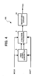
- the PWM signal generator 8 receives a main clock signal MCLK sent from a clock signal generator (not shown) and upper bits of the input data set DSET sent from a CPU (central processing unit) or the like (not shown).
- the PWM signal generator 8 performs a pulse width modulation for modulating the input data set DSET with a counter for counting the main clock signal MCLK, and outputs a resultant analog voltage and a PWM cycle signal to the fraction processor 9.
- the fraction processor 9 also receives the main clock signal MCLK and lower bits of the input data set DSET.
- the fraction processor 9 performs a PWM cycle division and, when a fraction is produced by the PWM cycle division, splits and distributes the fraction to each of the divided cycles.
- the fraction processor 9 outputs a resultant analog voltage.
- the smoothing circuit 10 smoothes the resultant analog voltage and outputs a desired analog voltage Vdac in response to a value of the input data set DSET.
- Fig. 5 shows further details of the structure of the DA converter 100.
- the DA converter 100 is provided with an eight bit counter (CUNT) 21, a magnitude comparator (COMP) 22, a data selector (SEL) 23, a selection signal generator (SSG) 24, a resister 25, and a capacitor 26.
- the selection signal generator 24 includes inverters 27 and 28, NAND gates 29 - 31, and an OR gate 32. Lower six bits Q0 - Q5 of the counter 21 and an output A > B of the comparator 22 configure the PWM signal generator 8 of Fig. 4.
- a cycle of the main clock MCLK is referred to as Tmclk, and an eight-bit counting cycle of the counter 21 is referred to as a pulse width modulation cycle Tpwm.
- the data set DSET is composed of eight data bits D0 - D7 and a cycle of the data set DSET is sufficiently longer than the pulse width modulation cycle Tpwm.
- the counter 21 counts the main clock signal MCLK and outputs each counting result from the outputs Q0 - Q7.
- the magnitude comparator 22 has input terminals B0 - B5 for receiving the outputs Q0 - Q5, respectively, and input terminals A0 - A5 for receiving upper six bits D2 - D7, respectively, of the data set DSET.
- the outputs Q6 and Q7 from the counter 21 and the lower two bits D0 and D1 of the data set DSET are connected to the selection signal generator 24.
- the magnitude comparator 22 outputs a high signal from the A>B output terminal when a value of the input terminals A0 - A5 is greater than that of the input terminals B0 - B5. Also, the magnitude comparator 22 outputs a high signal from the A ⁇ B output terminal when a value of the input terminals A0 - A5 is equal to or greater than that of the input terminals B0 - B5.
- the high signal from the A > B output terminal is input to an input terminal B of the data selection 23 and the high signal from the A ⁇ B output terminal is input to an input terminal A of the data selection 23.
- the data selector 23 enables the input terminal A when a selection terminal SELA is high and the input terminal B when SELA is low.
- the data selector 23 outputs a pulse signal Vpwm.
- the pulse signal Vpwm is smoothed by the smoothing circuit 10 composed of the resister 25 and the capacitor 26.
- the smoothing circuit 10 outputs a resultant analog voltage Vdac in response to the value of the data set DSET.
- Fig. 6 shows an example of the pulse signal Vpwm output from the smoothing circuit 10. This example is based on the resolution of eight bits (i.e., 1/256) and a four-way division of the pulse width modulation cycle Tpwm that is composed of 256 Tmclk. As shown in Fig. 6, each of pulse widths T1 - T4 of the pulse width modulation cycle Tpwm is 64 Tmclk.
- the pulse widths T1 - T4 in a high level are defined in the following manners, in which "int()" indicates an operation that a value enclosed by brackets is made an integer through a decimal round down, that is, a value smaller than a decimal point is rounded down, and DSET' is defined by DSET-int(DSET/4)x4.
- int() indicates an operation that a value enclosed by brackets is made an integer through a decimal round down, that is, a value smaller than a decimal point is rounded down
- DSET' is defined by DSET-int(DSET/4)x4.
- a difference between the maximum and the minimum of Th1 - Th4 is smaller than one Tmclk:
- Fig. 7 is a time chart showing a relationship between the pulse signal Vpwm and the analog voltage Vdac in two exemplary cases at the same time.
- the value of the data set DSET is set to 128, for example, and the related signal and waveform are labeled with a suffix numeral 128.
- the value of the data set DSET is set to 64, for example, and the related signal and waveform are labeled with a suffix numeral 64.
- Vpwm128 indicates as the pulse signal Vpwm in the case where the data set DSET is set to 128
- Vpwm64 indicates as the pulse signal Vpwm in the case where the data set DSET is set to 64.
- the pulse width modulation cycle Tpwm is divided into one fourth in the pulse width modulation, that is, a ripple frequency is increased to four times the ripple frequency of the DA converter according to the prior art.
- allowable variations of the analog voltage Vdac in high and low are supposed to remain same as those in the DA converter of the prior art. Accordingly, in the DA converter 100, the time constant of the RC circuit can be reduced to one fourth and consequently the response time can be reduced to one fourth.
- the pulse width modulation cycle Tpwm can be divided into an arbitrary number of time periods. However, it should be noted that the above-described structure is achieved when a division number is smaller than a value of 2 to the n minus one power, in which the n represents a number of bits of the DAC.
- the DA converter 200 includes a PWM (pulse width modulation) signal generator 8a, an amplitude regulator 15, a low-level regulator 16, a voltage adder 17, and the smoothing circuit 10.
- the smoothing circuit 10 is the one described in the discussion of the DA converter 100.
- the PWM signal generator 8a receives a main clock signal MCLK and lower bits of the input data set DSET.
- the PWM signal generator 8a performs a pulse width modulation relative to the input data set DSET with a counter for counting the main clock signal MCLK, and outputs a PWM signal to the amplitude regulator 15.
- the amplitude regulator 15 regulates an amplitude of the PWM signal and outputs a voltage to the voltage adder 17.
- the low-level regulator 16 regulates and outputs a relatively low level voltage to the voltage adder 17.
- the voltage adder 17 adds the voltage from the amplitude regulator 15 and the low-level voltage from the low-level regulator 16, and outputs a composite analog voltage to the smoothing circuit 10.
- the smoothing circuit smoothes the composite analog voltage and outputs a desired analog voltage Vdac in response to a value of the input data set DSET.
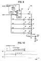
- Fig. 9 shows further details of the structure of the DA converter 200.
- the DA converter 200 is provided with a four-bit counter (CUNT) 221 for counting the main clock signal MCLK and a four-bit magnitude comparator (COMP) 222 for comparing an output from the four-bit counter 221 with the input data set DSET, which configure the PWM signal generator 8a of Fig. 8.
- the DA converter 200 further includes buffer elements 41 - 44 and resisters 45 - 52, which configure the amplitude regulator 15, the low-level regulator 16, and the voltage adder 17 of Fig. 8.
- the resisters 45 - 49 have a resistance value of 2R and the resisters 50 - 52 have a resistance value of R so that the resisters 45 - 52 in total form an R-2R ladder resister.
- the DA converter 200 further includes the resister 25 and the capacitor 26, configuring the smoothing circuit 10, as described above.
- a number of DAC bits is set to eight and a number of voltage levels for Vdac is set to sixteen.
- the magnitude comparator 222 outputs a high signal from an output terminal A > B when an input A is greater than an input B.
- the magnitude comparator 222 has input terminals A0 - A3 for receiving the lower bits D0 - D3, respectively, of the input data set DSET and input terminals B0 - B3 for receiving the outputs Q0 - Q3, respectively, of the counter 221.
- the upper bits D4-D7 of the input data set DSET are input to the buffer elements 41 - 44, respectively.
- the output A>B of the magnitude comparator 222 and the outputs of the buffer elements 41 - 44 are input to the R-2R ladder composed of the resisters 45 - 52.
- the R-2R ladder outputs a resultant pulse signal Vpwm which is smoothed by the smoothing circuit 10 composed of the resister 25 and the capacitor 26.
- a desired analog voltage Vdac is output in response to the input data set DSET.
- the resultant pulse signal Vpwm is varied in sixteen levels through the R-2R ladder in accordance with the output A > B of the magnitude comparator 222 and the output levels of the buffer elements 41 - 44. That is, the resultant pulse signal Vpwm is varied by following calculations:
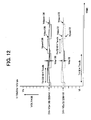
- Fig. 12 is a time chart showing a relationship between the pulse signal Vpwm and the analog voltage Vdac in two exemplary cases at the same time.
- the value of the data set DSET is set to 136, for example, and the related signal and waveform are labeled with a suffix numeral 136.
- the value of the data set DSET is set to 72, for example, and the related signal and waveform are labeled with a suffix numeral 72.
- Vpwm136 indicates as the pulse signal Vpwm in the case where the data set DSET is set to 136
- Vpwm72 indicates as the pulse signal Vpwm in the case where the data set DSET is set to 72.
- the pulse width modulation cycle Tpwm is divided into one sixteenth in the pulse width modulation, that is, a ripple frequency is increased to sixteen times the ripple frequency of the DA converter of the prior art.
- the difference between the voltges Vh and Vl is divided into sixteen levels.
- the difference between the voltages Vh and Vl can be divided into arbitrary levels. However, it should be noted that the above-described structure is achieved when a division number is smaller than a value of 2 to the n minus one power, in which the n represents a number of bits of the DAC.
- the R-2R ladder resister composed of resisters 45 - 52 may be integrated in an IC (integrated circuit) chip.
- the DA converter 300 includes the PWM signal generator 8, a fraction processor 9a, a level regulator 18, and the smoothing circuit 10.
- the PWM signal generator 8 receives a main clock signal MCLK and upper bits of the input data set DSET.
- the PWM signal generator 8 performs a pulse width modulation modulating the input data set DSET with a counter for counting the main clock signal MCLK, and outputs a resultant analog voltage and a PWM cycle signal to the fraction processor 9a.
- the fraction processor 9a also receives the main clock signal MCLK and lower bits of the input data set DSET.
- This fraction processor 9a performs a PWM cycle division and, when a fraction is produced by the PWM cycle division, splits and distributes the fraction to each of the divided cycles.
- the fraction processor 9a outputs multi-bit Pwm signals to the level regulator 18.
- the level regulator 18 regulates the level of the multi-bit Pwm signals.
- the smoothing circuit 10 smoothes the resultant analog voltage and outputs a desired analog voltage Vdac in response to a value of the input data set DSET.
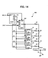
- Fig. 14 shows further details of the structure of the DA converter 300.
- the DA converter 300 is provided with a four-bit counter (CUNT) 321 for counting the main clock signal MCLK and a four-bit magnitude comparator (COMP) 322 for comparing an output from the four-bit counter 321 with the input data set DSET, which configure the PWM signal generator 8a of Fig. 10.
- the DA converter 300 further includes multiplexers (MPX#) 61 - 64 configuring the fraction processor 9a of Fig. 10 and the resisters 45 - 52 configuring the level regulator 18 of Fig. 10.
- the DA converter 300 further includes the resister 25 and the capacitor 26, configuring the smoothing circuit 10.
- the resisters 45 - 49 have a resistance value of 2R and the resisters 50 - 52 have a resistance value of R so that the resisters 45 - 52 in total form the R-2R ladder resister.
- the output A > B of the magnitude comparator 322 and the output Y of the MPX0 are assigned with a weight of 1/16.
- the outputs Y of the MPX1 - MPX3 are assigned with weights of 1/8, 1/4, and 1/2, respectively.
- a number of DAC bits is set to eight and a number of voltage levels for Vdac is set to sixteen.
- the magnitude comparator 322 outputs a high signal from an output terminal A > B when an input A is greater than an input B.
- the magnitude comparator 322 has input terminals A0 - A3 for receiving the upper bits D4 - D7, respectively, of the input data set DSET and input terminals B0 - B3 for receiving the outputs Q0 - Q3, respectively, of the counter 321.
- the lower bits D0-D3 of the input data set DSET are input to the multiplexers 61 - 64, respectively.
- the output CO (carry over) of the counter 321 is high when the outputs Q0 - Q3 are all high.
- the output CO is input to selection terminals SEL of the multiplexers 61 - 64 so that the multiplexers 61 - 64 select the output A>B when the output CO is low and the multiplexers 61 - 64 select the data of the lower bits D0 - D3 of DSET.
- the output A>B of the magnitude comparator 222 and the outputs of the multiplexers 61 - 64 constitute multi-bit pwm signals to be input to the R-2R ladder composed of the resisters 45 - 52.
- the R-2R ladder outputs a resultant pulse signal Vpwm which is smoothed by the smoothing circuit 10 composed of the resister 25 and the capacitor 26. As a result, a desired analog voltage Vdac is output in response to the input data set DSET.
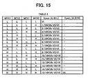
- the resultant pulse signal Vpwm is varied in sixteen levels through the R-2R ladder in accordance with the output A>B of the magnitude comparator 322 and the output levels of the multiplexers 61 - 64. That is, the resultant pulse signal Vpwm is varied by following calculations:
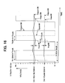
- Fig. 16 is a time chart showing a relationship between the pulse signal Vpwm and the analog voltage Vdac in two exemplary cases at the same time.
- the value of the data set DSET is set to 136, for example, and the related signal and waveform are labeled with a suffix numeral 136.
- the value of the data set DSET is set to 68, for example, and the related signal and waveform are labeled with a suffix numeral 68.
- Vpwm136 indicates as the pulse signal Vpwm in the case where the data set DSET is set to 136
- Vpwm68 indicates as the pulse signal Vpwm in the case where the data set DSET is set to 68.
- the pulse width modulation cycle Tpwm is divided into one sixteenth in the pulse width modulation, that is, a ripple frequency is increased to sixteen times the ripple frequency of the DA converter of the prior art.
- allowable variations of the analog voltage Vdac in high and low remain same as those in the DA converter of the prior art. Accordingly, in the DA converter 300, the time constant of the RC circuit can be reduced to one sixteenth and consequently the response time can be reduced to one sixteenth.
- the difference between the voltages Vh and Vl can be divided into arbitrary levels. However, it should be noted that the above-described structure is achieved when a division number is smaller than a value of 2 to the n minus one power, in which the n represents a number of bits of the DAC.
- the R-2R ladder resister composed of resisters 45 - 52 may be integrated in an IC (integrated circuit) chip.
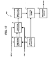
- the DA converter 400 includes a PWM (pulse width modulation) signal generator 8b, the fraction processor 9, the amplitude regulator 15, the low-level regulator 16, the voltage adder 17, and the smoothing circuit 10.
- the smoothing circuit 10 is the one described in the discussion of the DA converter 400.
- the PWM signal generator 8b receives a main clock signal MCLK and middle bits of the input data set DSET.
- the PWM signal generator 8b performs a pulse width modulation relative to the input data set DSET with a counter for counting the main clock signal MCLK, and outputs a PWM signal and a PWM cycle signal to the fraction processor 9.
- the fraction processor 9 also receives the main clock signal MCLK and low bits of the input data set DSET.
- the fraction processor 9 performs a PWM cycle division and, when a fraction is produced by the PWM cycle division, splits and distributes the fraction to each of the divided cycles.
- the fraction processor 9 outputs a resultant analog voltage to the amplitude regulator 15.
- the amplitude regulator 15 regulates an amplitude of the PWM signal and outputs a voltage to the voltage adder 17.
- the low-level regulator 16 regulates and outputs a relatively low level voltage to the voltage adder 17.
- the voltage adder 17 adds the voltage from the amplitude regulator 15 and the low-level voltage from the low-level regulator 16, and outputs a composite analog voltage to the smoothing circuit 10.
- the smoothing circuit 10 smoothes the composite analog voltage and outputs a desired analog voltage Vdac in response to a value of the input data set DSET.
- Fig. 18 shows further details of the structure of the DA converter 400.
- the DA converter 400 is provided with a four-bit counter (CUNT) 421 for counting the main clock signal MCLK and a two-bit magnitude comparator (COMP) 422 for comparing outputs Q0 and Q1 from the four-bit counter 421 with inputs D2 and D3 of the input data set DSET.
- the DA converter 400 further includes the selection signal generator 24 including the inverters 27 and 28, the NAND gates 29-31, and the OR gate 32.
- the lower two bits Q0 and Q1 of the counter 421 and the output A > B of the comparator 422 configure the PWM signal generator 8b of Fig. 17.
- the DA converter 400 further includes the buffer elements 41 - 44 and the resisters 45 - 52, which configure the amplitude regulator 15, the low-level regulator 16, and the voltage adder 17 of Fig. 17.
- the resisters 45 - 49 have a resistance value of 2R and the resisters 50 - 52 have a resistance value of R so that the resisters 45 - 52 in total form an R-2R ladder resister.
- the DA converter 400 further includes the resister 25 and the capacitor 26, configuring the smoothing circuit 10, as described above.
- the DA converter 400 In the DA converter 400, a number of DAC bits is set to eight, the upper four bits D4 - D7 of the input data set DSET are used for the low-level regulation, and the PWM cycle is divided into four cycles. That is, the DA converter 400 is a combination of the DA converter 100 and the DA converter 200.
- the magnitude comparator 422 outputs a high signal from an output terminal A > B when an input A is greater than an input B.
- the magnitude comparator 222 has input terminals A0 and A1 receiving the middle bits D2 and D3, respectively, of the input data set DSET and input terminals B0 and B1 receiving the outputs Q0 and Q1, respectively, of the counter 421.
- the upper two bits Q2 and Q3 and the lower bits D0 and D1 of the input data set DSET are input to the selection signal generator 24 which generates a selection signal and outputs it to the data selector 23.
- the high signal from the A > B output terminal is input to an input terminal B of the data selection 23 and the high signal from the A ⁇ B output terminal is input to an input terminal A of the data selection 23.
- the data selector 23 enables the input terminal A when a selection terminal SELA is high and the input terminal B when SELA is low.
- the data selector 23 outputs a pulse signal Vpwm.
- the upper bits D4 - D7 of the input data set DSET are input to the buffer elements 41 - 44, respectively.
- the output A>B of the magnitude comparator 422 and the outputs of the buffer elements 41 - 44 are input to the R-2R ladder composed of the resisters 45 - 52.
- the R-2R ladder outputs a resultant pulse signal Vpwm which is smoothed by the smoothing circuit 10 composed of the resister 25 and the capacitor 26. As a result, a desired analog voltage Vdac is output in response to the input data set DSET.
- Fig. 19 shows an example of the pulse signal Vpwm output from the smoothing circuit 10.
- the pulse width modulation cycle Tpwm is composed of 16 Tmclk and, as shown in Fig. 19, each of pulse widths T1 - T4 of the pulse width modulation cycle Tpwm is 4 Tmclk.
- the pulse widths T1 - T4 in a high level are defined in the following manners, in which "int()" indicates an operation that a value enclosed by brackets is made an integer through a decimal round down, that is, a value smaller than a decimal point is rounded down.
- a difference between the maximum and the minimum of Th1 - Th4 is smaller than one Tmclk:
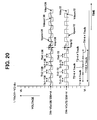
- Fig. 20 is a time chart showing a relationship among the pulse signal Vpwm, the analog voltage Vdac, and the ripple voltage Vrip when the value of the data set DSET is set to 136, for example, and when the value of the data set DSET is set to 72, for example, at the same time.
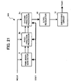
- the DA converter 500 includes the PWM (pulse width modulation) signal generator 8, a first fraction processor 9b, a second fraction processor 9c, the level regulator 18, and the smoothing circuit 10.
- PWM pulse width modulation
- the PWM signal generator 8 receives a main clock signal MCLK and upper bits of the input data set DSET.
- the PWM signal generator 8 performs a pulse width modulation relative to the input data set DSET with a counter for counting the main clock signal MCLK, and outputs a PWM signal and a PWM cycle signal to the first fraction processor 9b.
- the first fraction processor 9b also receives the main clock signal MCLK and middle bits of the input data set DSET.
- the first fraction processor 9b performs a PWM cycle division and outputs a divided PWM signal and a PWM cycle signal.
- the second fraction processor 9c receives the main clock signal, the lower bits of the input data set DSET, as well as the divided PWM signal and the PWM cycle signal.
- the second fraction processor 9c Based on these signals, the second fraction processor 9c outputs a multi-bit PWM signal.
- the level regulator 18 regulates the level of the multi-bit PWM signal and outputs an analog voltage to the smoothing circuit 10.
- the smoothing circuit 10 smoothes the analog voltage and outputs a desired analog voltage Vdac in response to a value of the input data set DSET.
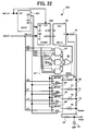
- Fig. 22 shows further details of the structure of the DA converter 500.
- the DA converter 500 is provided with a four-bit counter (CUNT) 521 for counting the main clock signal MCLK and a two-bit magnitude comparator (COMP) 522 for comparing outputs Q0 and Q1 from the four-bit counter 521 with inputs D6 and D7 of the input data set DSET.
- the DA converter 500 further includes the selection signal generator 24 including the inverters 27 and 28, the NAND gates 29-31, and the OR gate 32.
- the lower two bits Q0 and Q1 of the counter 521 and the output A > B of the comparator 522 configure the PWM signal generator 8 of Fig. 21.
- the DA converter 500 further includes the multiplexers (MPX#) 61 - 64 configuring the second fraction processor 9c of Fig. 21 and the resisters 45 - 52 configuring the level regulator 18 of Fig. 21.
- the resisters 45 - 49 have a resistance value of 2R and the resisters 50 - 52 have a resistance value of R so that the resisters 45 - 52 in total form an R-2R ladder resister.
- the DA converter 500 further includes the resister 25 and the capacitor 26, configuring the smoothing circuit 10, as described above.
- the DA converter 500 a number of DAC bits is set to eight, the upper four bits D4 - D7 of the input data set DSET are used for the four-way division of the Pwm cycle, and a unit width in a high state in response to the lower four bits D0 - D3 of the input data set DSET is added to the PWM cycle. That is, the DA converter 500 is a combination of the DA converter 100 and the DA converter 300.
- the magnitude comparator 522 outputs a high signal from an output terminal A > B when an input A is greater than an input B.
- the magnitude comparator 522 has input terminals A0 and A1 receiving the upper bits D6 and D7, respectively, of the input data set DSET and input terminals B0 and B1 receiving the outputs Q0 and Q1, respectively, of the counter 521.
- the upper two bits Q2 and Q3 and the middle bits D4 and D5 of the input data set DSET are input to the selection signal generator 24 which generates a selection signal and outputs it to the data selector 23.
- the high signal from the A > B output terminal is input to an input terminal B of the data selection 23 and the high signal from the A ⁇ B output terminal is input to an input terminal A of the data selection 23.
- the data selector 23 enables the input terminal A when a selection terminal SELA is high and the input terminal B when SELA is low.
- the data selector 23 outputs a pulse signal Vpwm.
- the lower bits D0 - D3 of the input data set DSET are input to the multiplexers 61 - 64, respectively.
- the output CO of the counter 521 is high when the outputs Q0 - Q3 are all high.
- the output CO is input to selection terminals SEL of the multiplexers 61 - 64 so that the multiplexers 61 - 64 select the output of the data selector 23 when the output CO is low and the multiplexers 61 - 64 select the data of the lower bits D0 - D3 of DSET.
- the output of the data selector 23 and the outputs of the multiplexers 61 - 64 are input to the R-2R ladder composed of the resisters 45 - 52.
- the R-2R ladder outputs a resultant pulse signal Vpwm which is smoothed by the smoothing circuit 10 composed of the resister 25 and the capacitor 26.
- a desired analog voltage Vdac is output in response to the input data set DSET.
- Fig. 23 is a time chart showing a relationship among the pulse signal Vpwm, the analog voltage Vdac, and the ripple voltage Vrip when the value of the data set DSET is set to 136, for example, and when the value of the data set DSET is set to 68, for example, at the same time.
- the Pwm cycle Tpwm is 16 Tmclk and each of the divided time lengths T1 - T4 is 4 Tmclk. Therefore, the DA converter 500 can reduce a time for holding a high level or a low level to 1/64 in comparison to those performances of the DA converter of the prior art. Since allowable variations of the analog voltage Vdac in high and low remain same as those in the DA converter of the prior art, the DA converter 500 can reduce the time constant of the RC circuit to 1/64 and consequently the response time can be reduced to 1/64.
- the DA converter according to the present invention may be used, for example, for a feed back circuit for adjusting a direct current (DC) level of an analog signal or a full-scale or zero-scale level of an analog-to-digital (AD) converter in a control for automatically adjusting a reading level of a reading mechanism in a digital copying machine, a scanner, or the like.
- the data set DSET applied to this DA converter is changed in a cycle sufficiently longer than the pulse width modulation cycle Tpwm.
- the present invention is not limited to this particular application and may be used instead in similar applications, e.g. in applications wherein a voltage level is to be adjusted automatically, as will become apparent to the person skilled in the art when studying the present application.
Landscapes
- Engineering & Computer Science (AREA)
- Theoretical Computer Science (AREA)
- Physics & Mathematics (AREA)
- General Engineering & Computer Science (AREA)
- General Physics & Mathematics (AREA)
- Analogue/Digital Conversion (AREA)
Abstract
Description
- Fig. 1
- is a schematic diagram of a digital-to-analog converter according to the prior art;
- Fig. 2
- is a time chart for explaining a pulse width modulation performed by the digital-to-analog converter of Fig. 1;
- Fig. 3
- is a time chart for explaining the pulse width modulation performed by the digital-to-analog converter of Fig. 1 when an input data set is 128 and 64;
- Fig. 4
- is a schematic block diagram of a digital-to-analog converter according to a preferred embodiment of the present invention;
- Fig. 5
- is a schematic circuit diagram of the digital-to-analog converter of Fig. 4;
- Fig. 6
- is a time chart for explaining a pulse width modulation performed by the digital-to-analog converter of Fig. 4;
- Fig. 7
- is a time chart for explaining the pulse width modulation performed by the digital-to-analog converter of Fig. 4 when an input data set is 128 and 64;
- Fig. 8
- is a schematic block diagram of a digital-to-analog converter according to another preferred embodiment of the present invention;
- Fig. 9
- is a schematic circuit diagram of the digital-to-analog converter of Fig. 8;
- Fig. 10
- is a time chart for explaining a pulse width modulation performed by the digital-to-analog converter of Fig. 8;
- Fig. 11
- is a table showing relationships among upper bits of the input data set, a pulse width modulation signal, and a condition signal referred to as an output A>B;
- Fig. 12
- is a time chart for explaining the pulse width modulation performed by the digital-to-analog converter of Fig. 8 when an input data set is 136 and 72;
- Fig. 13
- is a schematic block diagram of a digital-to-analog converter according to another preferred embodiment of the present invention;
- Fig. 14
- is a schematic circuit diagram of the digital-to-analog converter of Fig. 13;
- Fig. 15
- is a table showing relationships among values of multiplexers, a pulse width modulation signal, and a condition signal referred to as an output A > B;
- Fig. 16
- is a time chart for explaining the pulse width modulation performed by the digital-to-analog converter of Fig. 13 when an input data set is 136 and 68;
- Fig. 17
- is a schematic block diagram of a digital-to-analog converter according to another preferred embodiment of the present invention;
- Fig. 18
- is a schematic circuit diagram of the digital-to-analog converter of Fig. 17;
- Fig. 19
- is a time chart for explaining a pulse width modulation performed by the digital-to-analog converter of Fig. 17;
- Fig. 20
- is a time chart for explaining the pulse width modulation performed by the digital-to-analog converter of Fig. 17 when an input data set is 136 and 72;
- Fig. 21
- is a schematic block diagram of a digital-to-analog converter according to another preferred embodiment of the present invention;
- Fig. 22
- is a schematic circuit diagram of the digital-to-analog converter of Fig. 21; and
- Fig. 23
- is a time chart for explaining the pulse width modulation performed by the digital-to-analog converter of Fig. 17 when an input data set is 136 and 68.
- T1;
- Th1=int(DSET/4),
- T2;
- Th2=Th1+int(DSET'/3)xTmclk,
- T3;
- Th3 =Th1 + int(DSET'/2)xTmclk, and
- T4;
- Th4 = Th1 + DSET'-int(DSET'/2)x2xTmclk.
- T1;
- Th1=int(DSE'/4)xTmclk,
- T2;
- Th2=Th1+int(DSET"/3)xTmclk,
- T3;
- Th3=Th1+int(DSET"/2)xTmclk, and
- T4;
- Th4=Th1+DSET"-int(DSET"/2)x2xTmclk.
Claims (15)
- A digital-to-analog converter for converting n-bit digital data to an analog voltage, wherein n is an arbitrary integer and the n bits are composed at least of a first group of bits and of a second group of bits different from said first group of bits, said digital-to-analog converter (100, 200, 300, 400, 500) comprising:a signal generator (8) for performing a pulse width modulation based on inputs of a reference clock signal (MCLK) and the first group of bits of said n-bit digital data (DSET) and for generating a first pulse-width-modulated signal having a plurality of first pulses having a first pulse width in response to a value of the first group of bits of said n-bit digital data and a pwm cycle signal indicating a cycle of a pulse width modulation performed;a fraction processing means (9) receiving said pulse-width-modulated signal (Vpwm), said pwm cycle signal and the second group of bits of said n-bit digital data for dividing a pulse width in response to a value of the second group of bits of said n-bit digital data into a plurality of fraction pulse widths and for generating a second pulse-width-modulated signal having a plurality (Vpwm 128) of second pulses based on said plurality of fraction pulse widths; anda voltage smoothing circuit (24, 25) for smoothing an analog signal comprising said second pulse-width-modulated signal.
- The digital-to-analog converter according to claim 1, wherein said first group of bits represents upper nh bits of said n-bit digital data and said second group of bits represents lower nl bits of said n-bit digital data, wherein
said signal generator (8) is arranged and configured to perform a pulse width modulation based on inputs of a reference clock signal and the upper nh bits (nh) of said n-bit digital data (DSET) and to generate a first pulse-width-modulated signal having a plurality of first pulses having a first pulse width in response to a value of the upper nh bits (nh) of said n-bit digital data and a pwm cycle signal indicating a cycle of a pulse width modulation performed;
said first fraction processing means (9) is arranged and configured to divide a pulse width in response to a value of the lower nl bits of said n-bit digital data into a plurality of fraction pulse widths, to respectively add said plurality of fraction pulse widths to said plurality of first pulses and to generate said second pulse-width-modulated signal having a plurality of second pulses having said first pulse width and one of said plurality of fraction pulse widths; and wherein
said voltage smoothing circuit (10) is arranged and configured to smooth said second pulse-width-modulated signal. - The digital-to-analog converter according to claim 2, wherein
said signal generator (8) is configured of lower six bits (Q0-Q5) of a counting means (21) and an output (A > B) of a comparator means (22), and
said first fraction processing means (9) is configured of upper two bits (Q6, Q7) of said counting means, an output (A ≥ B) of said comparator means (22), a data selector (23), inverting means (27, 28) and logic gate means (29-32). - The digital-to-analog converter according to claim 1, wherein said first group of bits represents upper nh bits of said n-bit digital data and said second group of bits represents lower nl bits of said n-bit digital data, wherein
said signal generator (8) is arranged and configured to perform a pulse width modulation based on inputs of a reference clock signal and the upper nh bits (nh) of said n-bit digital data (DSET) and to generate a first pulse-width-modulated signal having a plurality of first pulses having a first pulse width in response to a value of the upper nh bits (nh) of said n-bit digital data and a pwm cycle signal indicating a cycle of a pulse width modulation performed;
said first fraction processing means is arranged and configured to generate, as said second pulse-width-modulated signal, multi-bit pulse-width-modulated signals including said pulse-width-modulated signal as a least significant bit and the lower nl bits of said n-bit digital data;
said digital-to-analog converter (300) further comprising:a level regulator (18) arranged and configured to receive said multi-bit pulse-width-modulated signals and to output an analog voltage with an upper level regulated in response to a value of said multi-bit pulse-width-modulated signals; whereinsaid voltage smoothing circuit (10) is arranged and configured to smooth said analog voltage output by said level regulator (18). - The digital-to-analog converter according to claim 4, wherein
said first fraction processing means (9a) comprises multiplexers (61-64) and
said level regulator (18) comprises first resistors (50-52) having a first resistance value (R) and second resistors (45-49) having a second resistance value (2R) twice said first resistance value, said first and second resistors forming a ladder resistor, wherein
outputs of said multiplexers (61-64) are assigned to weights of said ladder resistor. - The digital-to-analog converter according to claim 1, wherein the n bits are composed of said first group of bits representing upper nh bits of said n-bit digital data, of said second group of bits representing middle nm bits of said n-bit digital data, and of a third group of bits representing lower nl bits of said n-bit digital data, wherein
said signal generator (8b) is arranged and configured to perform a pulse width modulation based on inputs of a reference clock signal and the middle nm bits of said n-bit digital data (DSET) and to generate a first pulse-width-modulated signal having a plurality of first pulses having a first pulse width in response to a value of the middle nm bits (nm) of said n-bit digital data and a pwm cycle signal indicating a cycle of a pulse width modulation performed;
said first fraction processing means (9) is arranged and configured to receive said pulse-width-modulated signal, said pwm cycle signal, and the lower nl bits of said n-bit digital data for dividing a pulse width in response to a value of the lower nl bits (nl) of said n-bit digital data into a plurality of fraction pulse widths, for respectively adding said plurality of fraction pulse widths to said plurality of first pulses and for generating a second pulse-width-modulated signal having a plurality of second pulses having said first pulse width and one of said plurality of fraction pulse widths;
said digital-to-analog converter (400) further comprising:an amplitude regulator (15) for regulating an amplitude of said second pulse-width-modulated signal generated by said signal generator;a bottom-level regulator (16) receiving the upper nh bits (nh) of said n-bit digital data for regulating a bottom level of a voltage in accordance with a value of said upper nh bits (nh) of said n-bits digital data; anda voltage adding circuit (17) for adding said second pulse-width-modulated signal having an amplitude regulated by said amplitude regulator (15) to said voltage having a bottom level regulated by said bottom-level regulator (16) and for outputting a composite voltage; whereinsaid voltage smoothing circuit (10) is arranged and configured to smooth said composite voltage output by said voltage adding circuit (17). - The digital-to-analog converter according to claim 6, wherein
said signal generator (8b) is configured of lower two bits (Q0, Q1) of a conting means (421) and an output (A > B) of a comparator means (422),
said first fraction processing means (9) is configured of upper two bits (Q2, Q3) of said counting means (421), an output (A ≥ B) of said comparator means (422), a data selecting means (23) and a selection signal generating means (24). - The digital-to-analog converter according to claim 1, wherein the n bits are composed of a first group of bits representing upper nh bits of said n-bit digital data, of a second group of bits representing middle nm bits of said n-bit digital data and of a third group of bits representing lower nl bits of said n-bit digital data, wherein
said signal generator (8) is arranged and configured to perform a pulse width modulation based on inputs of a reference clock signal and the upper nh bits (nh) of said n-bit digital data (DSET) and to generate a first pulse-width-modulated signal having a plurality of first pulses having a first pulse width in response to a value of the upper nh bits (nh) of said n-bit digital data and a pwm cycle signal indicating a cycle of a pulse width modulation performed;
said first fraction processing means (9b) is arranged and configured to receive said pulse-width-modulated signal, said pwm cycle signal, and the middle nm bits (nm) of said n-bit digital data, for dividing a pulse width in response to a value of the middle nm bits (nm) of said n-bit digital data into a plurality of fraction pulse widths, for respectively adding said plurality of fraction pulse widths to said plurality of first pulses and for generating a second pulse-width-modulated signal having a plurality of second pulses having said first pulse width and one of said plurality of fraction pulse widths;
said digital-to-analog converter (500) further comprising:a second fraction processing means (9c) receiving said second pulse-width-modulated signal, said pwm cycle signal, and the lower nl bits (nl) of said n-bit digital data, for generating multi-bit pulse-width-modulated signals including said second pulse-width-modulated signal as a least significant bit and the lower nl bits of said n-bit digital data; anda level regulator (18) for receiving said multi-bit pulse-width-modulated signals and outputting an analog voltage with an upper level regulated in response to a value of said multi-bit pulse-width-modulated signals; whereinsaid voltage smoothing circuit (10) is arranged and configured to smooth said analog voltage output by said level regulator (18). - The digital-to-analog converter according to claim 8, wherein
said first fraction processing means (9b) is configured of upper two bits (Q2, Q3) of a counting means (521), an output (A ≥ B) of a comparator means (522), a data selecting means (23) and a selection signal generating means (24),
said second fraction processing means (9c) is configured of multiplexers (61-64) and
said level regulator (18) comprises first resistors (50-52) having a first resistance value (R) and second resistors (45-49) having a second resistance value (2R) twice said first resistance value, said first and second resistors forming a ladder resistor, wherein
outputs of said multiplexers (61-64) are assigned to weights of said ladder resistor. - A digital-to-analog converter for converting n-bit digital data to an analog voltage, wherein n is an arbitrary integer and the n bits are composed of upper nh bits and lower nl bits, said digital-to-analog converter (200) comprising:a signal generator (8a) for performing a pulse width modulation based on inputs of a reference clock signal and the lower nl bits of said n-bit digital data and generating a pulse-width-modulated signal having a plurality of first pulses having a first pulse width in response to a value of the lower nh bits of said n-bit digital data;an amplitude regulator (15) for regulating an amplitude of said pulse-width-modulated signal generated by said signal generator;a bottom-level regulator (16) receiving the upper nh bits of said n-bit digital data for regulating a bottom level of a voltage in accordance with a value of said upper nh bits of said n-bits digital data;a voltage adding circuit (17) for adding said pulse-width-modulated signal having an amplitude regulated by said amplitude regulator to said voltage having a bottom level regulated by said bottom-level regulator and outputting a composite voltage; anda voltage smoothing circuit (10) for smoothing said composite voltage output by said voltage adding circuit (17).
- A method of digital-to-analog conversion for converting n-bit digital data to an analog voltage, wherein n is an arbitrary integer and the n bits are composed of upper nh bits and lower nl bits, said digital-to-analog converter comprising the steps of:performing a pulse width modulation based on inputs of a reference clock signal and the upper nh bits of said n-bit digital data to generate a first pulse-width-modulated signal having a plurality of first pulses having a first pulse width in response to a value of the upper nh bits of said n-bit digital data and a pwm cycle signal indicating a cycle of a pulse width modulation performed;dividing a pulse width in response to a value of the lower nl bits of said n-bit digital data into a plurality of fraction pulse widths;adding respectively said plurality of fraction pulse widths to said plurality of first pulses to output a second pulse-width-modulated signal having a plurality of second pulses having said first pulse width and one of said plurality of fraction pulse widths; andsmoothing said second pulse-width-modulated signal output in said adding step.
- A method of digital-to-analog conversion for converting n-bit digital data to an analog voltage, wherein n is an arbitrary integer and the n bits are composed of upper nh bits and lower nl bits, said digital-to-analog converter comprising the steps of:performing a pulse width modulation based on inputs of a reference clock signal and the lower nl bits of said n-bit digital data to generate a pulse-width-modulated signal having a plurality of first pulses having a first pulse width in response to a value of the lower nh bits of said n-bit digital data;regulating an amplitude of said pulse-width-modulated signal generated in said performing step;determining a bottom level of a voltage in accordance with a value of said upper nh bits of said n-bits digital data;adding said pulse-width-modulated signal having an amplitude regulated in said regulating step to said voltage having a bottom level determined in said determining step to output a composite voltage; andsmoothing said composite voltage output in said adding step.
- A method of digital-to-analog conversion for converting n-bit digital data to an analog voltage, wherein n is an arbitrary integer and the n bits are composed of upper nh bits and lower nl bits, said digital-to-analog converter comprising the steps of:performing a pulse width modulation based on inputs of a reference clock signal and the upper nh bits of said n-bit digital data to generate a first pulse-width-modulated signal having a plurality of first pulses having a first pulse width in response to a value of the upper nh bits of said n-bit digital data and a pwm cycle signal indicating a cycle of a pulse width modulation performed;generating multi-bit pulse-width-modulated signals including said pulse-width-modulated signal as a least significant bit and the lower nl bits of said n-bit digital data;outputting an analog voltage with an upper level regulated in response to a value of said multi-bit pulse-width-modulated signals; andsmoothing said analog voltage output in said outputting step.
- A method of digital-to-analog conversion for converting n-bit digital data to an analog voltage, wherein n is an arbitrary integer and the n bits are composed of upper nh bits, middle nm bits, and lower nl bits, said digital-to-analog converter comprising the steps of:performing a pulse width modulation based on inputs of a reference clock signal and the middle nm bits of said n-bit digital data to generate a first pulse-width-modulated signal having a plurality of first pulses having a first pulse width in response to a value of the middle nm bits of said n-bit digital data and a pwm cycle signal indicating a cycle of a pulse width modulation performed;dividing a pulse width in response to a value of the lower nl bits of said n-bit digital data into a plurality of fraction pulse widths;adding respectively said plurality of fraction pulse widths to said plurality of first pulses to generate a second pulse-width-modulated signal having a plurality of second pulses having said first pulse width and one of said plurality of fraction pulse widths;regulating an amplitude of said second pulse-width-modulated signal generated in said adding step;determining a bottom level of a voltage in accordance with a value of said upper nh bits of said n-bits digital data;overlaying said second pulse-width-modulated signal having an amplitude regulated in said regulating step to said voltage having a bottom level determined in said determining step to output a composite voltage; andsmoothing said composite voltage output in said overlaying step.
- A method of digital-to-analog conversion for converting n-bit digital data to an analog voltage, wherein n is an arbitrary integer and the n bits are composed of upper nh bits, middle nm bits, and lower nl bits, said digital-to-analog converter comprising the steps of:performing a pulse width modulation based on inputs of a reference clock signal and the upper nh bits of said n-bit digital data to generate a first pulse-width-modulated signal having a plurality of first pulses having a first pulse width in response to a value of the upper nh bits of said n-bit digital data and a pwm cycle signal indicating a cycle of a pulse width modulation performed;dividing a pulse width in response to a value of the middle nm bits of said n-bit digital data into a plurality of fraction pulse widths;adding respectively said plurality of fraction pulse widths to said plurality of first pulses to generate a second pulse-width-modulated signal having a plurality of second pulses having said first pulse width and one of said plurality of fraction pulse widths;generating multi-bit pulse-width-modulated signals including said second pulse-width-modulated signal as a least significant bit and the lower nl bits of said n-bit digital data;outputting an analog voltage with an upper level regulated in response to a value of said multi-bit pulse-width-modulated signals; andsmoothing said analog voltage output in said outputting step.
Applications Claiming Priority (4)
| Application Number | Priority Date | Filing Date | Title |
|---|---|---|---|
| JP2001081217 | 2001-03-21 | ||
| JP2001081217 | 2001-03-21 | ||
| JP2002023245A JP4073676B2 (en) | 2001-03-21 | 2002-01-31 | DA converter and DA conversion method |
| JP2002023245 | 2002-01-31 |
Publications (3)
| Publication Number | Publication Date |
|---|---|
| EP1244219A2 true EP1244219A2 (en) | 2002-09-25 |
| EP1244219A3 EP1244219A3 (en) | 2003-08-06 |
| EP1244219B1 EP1244219B1 (en) | 2007-01-03 |
Family
ID=26611707
Family Applications (1)
| Application Number | Title | Priority Date | Filing Date |
|---|---|---|---|
| EP02006572A Expired - Lifetime EP1244219B1 (en) | 2001-03-21 | 2002-03-21 | Method and apparatus for digital-to-analog conversion with an effective pulse width modulation |
Country Status (4)
| Country | Link |
|---|---|
| US (1) | US6606046B2 (en) |
| EP (1) | EP1244219B1 (en) |
| JP (1) | JP4073676B2 (en) |
| DE (1) | DE60217212T2 (en) |
Cited By (1)
| Publication number | Priority date | Publication date | Assignee | Title |
|---|---|---|---|---|
| WO2004051860A3 (en) * | 2002-11-29 | 2004-09-02 | Volker Schindler | Transmission configuration for transmitting signals and d/a converter circuits therefor |
Families Citing this family (20)
| Publication number | Priority date | Publication date | Assignee | Title |
|---|---|---|---|---|
| TW453045B (en) * | 2000-10-09 | 2001-09-01 | Winbond Electronics Corp | Multi-level pulse width modulation device and its control structure |
| JP2004048265A (en) * | 2002-07-10 | 2004-02-12 | Ricoh Co Ltd | Document reading device and image forming device |
| US6798369B1 (en) * | 2003-08-08 | 2004-09-28 | Visteon Global Technologies, Inc. | Precision, wide band pulse width modulator for digital to analog conversion |
| US7242330B2 (en) * | 2003-12-17 | 2007-07-10 | Texas Instruments Incorporated | Dynamic compensation of analog-to-digital converter (ADC) offset errors using filtered PWM |
| DE102004011723A1 (en) * | 2004-03-10 | 2005-09-29 | Patent-Treuhand-Gesellschaft für elektrische Glühlampen mbH | Digital-to-analogue converter with nested pulse width modulated signal |
| US7271754B2 (en) * | 2005-02-22 | 2007-09-18 | The Regents Of The University Of Colorado, A Body Corporate | Digital pulse-width modulator |
| TWI316794B (en) | 2006-06-15 | 2009-11-01 | Mstar Semiconductor Inc | Digital-to-analog converter and related method |
| US7724161B1 (en) * | 2006-12-12 | 2010-05-25 | Marvell International Ltd. | Truncation for three-level digital amplifier |
| TWI357220B (en) * | 2008-08-07 | 2012-01-21 | Generalplus Technology Inc | Low cost analog to digital converter and method fo |
| RU2433528C2 (en) * | 2009-07-28 | 2011-11-10 | Государственное образовательное учреждение высшего профессионального образования Пензенская государственная технологическая академия | Digital-to-analogue converter |
| RU2420867C2 (en) * | 2009-07-28 | 2011-06-10 | Государственное образовательное учреждение высшего профессионального образования "Пензенская государственная технологическая академия" | Method for digital-to-analogue conversion |
| JP6549366B2 (en) | 2014-09-19 | 2019-07-24 | 株式会社リコー | PHOTOELECTRIC CONVERSION ELEMENT, IMAGE READER, AND IMAGE FORMING APPARATUS |
| JP6612492B2 (en) | 2014-10-16 | 2019-11-27 | 株式会社リコー | Photoelectric conversion element, image reading apparatus, and image forming apparatus |
| US10913550B2 (en) | 2018-03-23 | 2021-02-09 | The Boeing Company | System and method for position and speed feedback control |
| US10911061B2 (en) * | 2018-03-23 | 2021-02-02 | The Boeing Company | System and method for demodulation of resolver outputs |
| US10830591B2 (en) | 2018-03-23 | 2020-11-10 | The Boeing Company | System and method for dual speed resolver |
| US10673368B2 (en) * | 2018-03-23 | 2020-06-02 | The Boeing Company | System and method for pulse-width modulation using an adjustable comparison criterion |
| CN111342954B (en) * | 2018-12-19 | 2022-09-23 | 科大国盾量子技术股份有限公司 | Random pulse generating system |
| CN114035480A (en) * | 2021-11-16 | 2022-02-11 | 西安西电电力系统有限公司 | Pulse generator based on C51 microcontroller |
| CN121566896B (en) * | 2026-01-26 | 2026-04-28 | 杭州极弱磁场国家重大科技基础设施研究院 | Method and apparatus for bias current adjustment |
Family Cites Families (7)
| Publication number | Priority date | Publication date | Assignee | Title |
|---|---|---|---|---|
| US4095218A (en) * | 1976-08-30 | 1978-06-13 | International Business Machines Corporation | Hybrid pulse width-pulse rate digital-to-analog converter method and apparatus |
| DE3208287A1 (en) * | 1982-03-08 | 1983-09-15 | Licentia Patent-Verwaltungs-Gmbh, 6000 Frankfurt | Circuit arrangement for converting a data word |
| JPS60219817A (en) * | 1984-04-16 | 1985-11-02 | Ricoh Co Ltd | Digital-analog converter |
| JPS6374664A (en) * | 1986-09-18 | 1988-04-05 | Sony Corp | Drive circuit of thermal head |
| JPH0353042A (en) | 1989-07-20 | 1991-03-07 | Sumitomo Metal Ind Ltd | Roll for rolling |
| US5157351A (en) | 1991-08-28 | 1992-10-20 | Sgs-Thomson Microelectronics, Inc. | Insulated gate enhancement mode field effect transistor with slew-rate control on drain output |
| JP3090200B2 (en) * | 1997-11-14 | 2000-09-18 | 日本電気株式会社 | Pulse width modulator |
-
2002
- 2002-01-31 JP JP2002023245A patent/JP4073676B2/en not_active Expired - Fee Related
- 2002-03-21 EP EP02006572A patent/EP1244219B1/en not_active Expired - Lifetime
- 2002-03-21 US US10/101,914 patent/US6606046B2/en not_active Expired - Fee Related
- 2002-03-21 DE DE60217212T patent/DE60217212T2/en not_active Expired - Lifetime
Cited By (1)
| Publication number | Priority date | Publication date | Assignee | Title |
|---|---|---|---|---|
| WO2004051860A3 (en) * | 2002-11-29 | 2004-09-02 | Volker Schindler | Transmission configuration for transmitting signals and d/a converter circuits therefor |
Also Published As
| Publication number | Publication date |
|---|---|
| JP4073676B2 (en) | 2008-04-09 |
| US6606046B2 (en) | 2003-08-12 |
| DE60217212T2 (en) | 2007-10-18 |
| EP1244219A3 (en) | 2003-08-06 |
| US20020149505A1 (en) | 2002-10-17 |
| DE60217212D1 (en) | 2007-02-15 |
| JP2002353814A (en) | 2002-12-06 |
| EP1244219B1 (en) | 2007-01-03 |
Similar Documents
| Publication | Publication Date | Title |
|---|---|---|
| EP1244219A2 (en) | Method and apparatus for digital-to-analog conversion with an effective pulse width modulation | |
| KR100318441B1 (en) | analog-digital converting apparatus and converting method thereof | |
| CA2004317C (en) | Successive comparison type analog-to-digital converting apparatus | |
| US4388612A (en) | Signal converter | |
| US6498577B1 (en) | Piecewise-linear, non-uniform ADC | |
| US20130082852A1 (en) | Analog to digital converter | |
| NL8007088A (en) | DIGITAL DITHER GENERATOR. | |
| EP0289081A1 (en) | Digital-to-analog converter | |
| RU2389133C1 (en) | Parallel analog-digital converter of dynamic type (versions) | |
| US5455583A (en) | Combined conventional/neural network analog to digital converter | |
| KR100235465B1 (en) | Flash-type analog-to-digital converter | |
| JP3407851B2 (en) | Delta-sigma D / A converter with PWM circuit / weighting circuit combination | |
| US6476747B1 (en) | Digital to analog converter | |
| JP3344524B2 (en) | D / A converter | |
| JPH08116258A (en) | Analog-digital conversion circuit | |
| JP7217116B2 (en) | analog/digital converter | |
| JP4519475B2 (en) | A / D converter | |
| JP2721450B2 (en) | Analog-digital conversion circuit | |
| JPS6352808B2 (en) | ||
| KR100261997B1 (en) | Analog-digital converter | |
| JPH05206858A (en) | DA conversion method | |
| KR20000003449A (en) | Device for converting analog-digital and converting method thereof | |
| JP3114795B2 (en) | High-speed AD converter | |
| JP2778286B2 (en) | D / A converter circuit | |
| KR100471787B1 (en) | Analog-digital converter for liquid crystal dispaly |
Legal Events
| Date | Code | Title | Description |
|---|---|---|---|
| PUAI | Public reference made under article 153(3) epc to a published international application that has entered the european phase |
Free format text: ORIGINAL CODE: 0009012 |
|
| AK | Designated contracting states |
Kind code of ref document: A2 Designated state(s): AT BE CH CY DE DK ES FI FR GB GR IE IT LI LU MC NL PT SE TR |
|
| AX | Request for extension of the european patent |
Free format text: AL;LT;LV;MK;RO;SI |
|
| RAP1 | Party data changed (applicant data changed or rights of an application transferred) |
Owner name: RICOH COMPANY LTD. |
|
| PUAL | Search report despatched |
Free format text: ORIGINAL CODE: 0009013 |
|
| AK | Designated contracting states |
Designated state(s): AT BE CH CY DE DK ES FI FR GB GR IE IT LI LU MC NL PT SE TR |
|
| AX | Request for extension of the european patent |
Extension state: AL LT LV MK RO SI |
|
| 17P | Request for examination filed |
Effective date: 20030826 |
|
| AKX | Designation fees paid |
Designated state(s): DE FR GB |
|
| 17Q | First examination report despatched |
Effective date: 20050224 |
|
| GRAP | Despatch of communication of intention to grant a patent |
Free format text: ORIGINAL CODE: EPIDOSNIGR1 |
|
| GRAS | Grant fee paid |
Free format text: ORIGINAL CODE: EPIDOSNIGR3 |
|
| GRAA | (expected) grant |
Free format text: ORIGINAL CODE: 0009210 |
|
| AK | Designated contracting states |
Kind code of ref document: B1 Designated state(s): DE FR GB |
|
| REG | Reference to a national code |
Ref country code: GB Ref legal event code: FG4D |
|
| REF | Corresponds to: |
Ref document number: 60217212 Country of ref document: DE Date of ref document: 20070215 Kind code of ref document: P |
|
| ET | Fr: translation filed | ||
| PLBE | No opposition filed within time limit |
Free format text: ORIGINAL CODE: 0009261 |
|
| STAA | Information on the status of an ep patent application or granted ep patent |
Free format text: STATUS: NO OPPOSITION FILED WITHIN TIME LIMIT |
|
| 26N | No opposition filed |
Effective date: 20071005 |
|
| REG | Reference to a national code |
Ref country code: FR Ref legal event code: PLFP Year of fee payment: 15 |
|
| REG | Reference to a national code |
Ref country code: FR Ref legal event code: PLFP Year of fee payment: 16 |
|
| PGFP | Annual fee paid to national office [announced via postgrant information from national office to epo] |
Ref country code: FR Payment date: 20170322 Year of fee payment: 16 Ref country code: DE Payment date: 20170322 Year of fee payment: 16 |
|
| PGFP | Annual fee paid to national office [announced via postgrant information from national office to epo] |
Ref country code: GB Payment date: 20170322 Year of fee payment: 16 |
|
| REG | Reference to a national code |
Ref country code: DE Ref legal event code: R119 Ref document number: 60217212 Country of ref document: DE |
|
| GBPC | Gb: european patent ceased through non-payment of renewal fee |
Effective date: 20180321 |
|
| PG25 | Lapsed in a contracting state [announced via postgrant information from national office to epo] |
Ref country code: DE Free format text: LAPSE BECAUSE OF NON-PAYMENT OF DUE FEES Effective date: 20181002 |
|
| PG25 | Lapsed in a contracting state [announced via postgrant information from national office to epo] |
Ref country code: GB Free format text: LAPSE BECAUSE OF NON-PAYMENT OF DUE FEES Effective date: 20180321 |
|
| PG25 | Lapsed in a contracting state [announced via postgrant information from national office to epo] |
Ref country code: FR Free format text: LAPSE BECAUSE OF NON-PAYMENT OF DUE FEES Effective date: 20180331 |