EP1244192A2 - Bicycle battery charger and speedometer circuit - Google Patents
Bicycle battery charger and speedometer circuit Download PDFInfo
- Publication number
- EP1244192A2 EP1244192A2 EP02251979A EP02251979A EP1244192A2 EP 1244192 A2 EP1244192 A2 EP 1244192A2 EP 02251979 A EP02251979 A EP 02251979A EP 02251979 A EP02251979 A EP 02251979A EP 1244192 A2 EP1244192 A2 EP 1244192A2
- Authority
- EP
- European Patent Office
- Prior art keywords
- signals
- dynamo
- circuit
- capacitor
- voltage
- Prior art date
- Legal status (The legal status is an assumption and is not a legal conclusion. Google has not performed a legal analysis and makes no representation as to the accuracy of the status listed.)
- Granted
Links
Images


Classifications
-
- H—ELECTRICITY
- H02—GENERATION; CONVERSION OR DISTRIBUTION OF ELECTRIC POWER
- H02J—CIRCUIT ARRANGEMENTS OR SYSTEMS FOR SUPPLYING OR DISTRIBUTING ELECTRIC POWER; SYSTEMS FOR STORING ELECTRIC ENERGY
- H02J7/00—Circuit arrangements for charging or depolarising batteries or for supplying loads from batteries
- H02J7/14—Circuit arrangements for charging or depolarising batteries or for supplying loads from batteries for charging batteries from dynamo-electric generators driven at varying speed, e.g. on vehicle
- H02J7/1407—Circuit arrangements for charging or depolarising batteries or for supplying loads from batteries for charging batteries from dynamo-electric generators driven at varying speed, e.g. on vehicle on vehicles not being driven by a motor, e.g. bicycles
Definitions
- the present invention is directed to bicycles and, more particularly, to a circuit that receives signals from a dynamo and provides signals for charging a battery and indicating bicycle speed.
- Bicycles often are equipped with dynamos for powering headlights and other types of lights. Contemporary bicycles, however, are equipped not only with such lights but also with actuators for operating electrically driven shifters, actuators for adjusting the dampening force of an electrically driven suspension, indicator backlights for cycle computers, and the like. Such equipment will be referred to below as “electrically driven units”, and they also receive their power from the dynamo. These electrically driven units begin operating unstably when their electric drive voltage falls below a specific level, so some accommodation must be made for supplying stable electric drive voltage to them. In late-model bicycles, a dynamo charges a secondary battery which, in turn, powers the electrically driven units.
- the present inventor has already devised and proposed an apparatus that allows the charging voltage to be detected and a stabilized charging voltage to be obtained through appropriate switching of the dynamo output.
- Speedometers are sometimes mounted on bicycles. Such speedometers operate with speed detection signals such as signals from a sensor that senses signals from a magnet mounted to the bicycle wheel.
- a technique for retrieving speed detection signals from a dynamo output is disclosed in JP (Kokai) 7-229909.
- JP (Kokai) 7-229909 JP (Kokai) 7-229909.
- the dynamo output is switched in a controlled manner in order to control the charging voltage, the voltage drop varies significantly because of the presence of a load resistance, an impedance or inductance in the dynamo, or the like.
- the switching also induces substantial disruptions in the output waveform of the dynamo.
- Low-pass filters and other circuits are needed in order to obtain a speed detection signal from a signal whose waveform is markedly disrupted in this manner, thus increasing the size and cost of the device.
- the present invention is directed to a comparatively simple circuit that receives signals from a dynamo and provides stable signals for charging a battery and indicating bicycle speed.
- a circuit includes a first switching circuit adapted to receive the dynamo signals and provide first signals for charging the battery; and a second switching circuit adapted to receive the dynamo signals and provide second signals for indicating bicycle speed.
- the first signals may correspond to one of the half periods of the periodic signals (e.g., the positive half periods), and the second signals may correspond to the other half periods (e.g., the negative half periods) of the periodic signals.
- a third switching circuit may be provided for selectively inhibiting the output of the first signals to the battery until the circuit is sufficiently stable, and a pulse signal circuit may be provided for producing pulse signals from the second signals to facilitate the operation of the speedometer.
- Fig. 1 is a conceptual schematic diagram of a particular embodiment of a battery charging and speed indicating circuit according to the present invention.
- the circuit comprises a dynamo 1 (generator), a first rectifying circuit 2 (first switching circuit), a second rectifying circuit 6 (second switching circuit), a secondary battery 3 (e.g., a capacitor) as a power supply for electrically driven units, and a switch 5 (third switching circuit) disposed between the dynamo 1 and the secondary battery 3.
- the circuit further comprises and a Schmitt circuit 7 coupled to the second rectifying circuit 6 for waveform shaping.
- the dynamo 1 may, for example, be a hub dynamo built into the hub of the bicycle front wheel, and it is provided with an internal impedance R and an internal inductance L.
- the rectifying circuit 2 contains diodes or the like to rectify the alternating-current voltage output by the dynamo 1 and to provide the secondary battery 3 with the resulting positive or negative (e.g., positive) half-periods.
- the switch 5 contains capacitors, transistors or the like for selectively inhibiting the communication of the signals from rectifying circuit 2 to battery 3.
- the second rectifying circuit 6 contains diodes or the like to rectify the alternating-current voltage output by the dynamo 1 and to provide the speedometer circuit (not shown) with the resulting positive or negative (e.g., negative) half-periods as a speed detection signal.
- the Schmitt circuit 7 receives the output of the second rectifying circuit 6 and outputs a pulse signal such as the one shown in Fig. 1 to facilitate the operation of the speedometer, which usually comprises a microcomputer.
- the signal waveforms of the various components of the circuit shown in Fig. 1 will now be described.
- the switch 5 is open or closed in accordance with the charging voltage of the secondary battery 3.
- the switching operation causes the load resistance to change abruptly, thus markedly varying the voltage drop due to the effect of the internal impedance R or internal inductance L of the dynamo 1.
- the dynamo output waveform is thereby disrupted violently as shown in Fig. 1.
- the output waveform is disrupted only during the positive half-periods because charging occurs only during these half-periods.
- a low-pass filter or other circuit is needed to derive a speed detection signal from such a disrupted output waveform.
- the present embodiment is configured such that the second rectifying circuit 6 retrieves the negative half-periods of the output provided by the dynamo 1, and the signal waveform is shaped to provide a pulse signal for speed detection. As shown in Fig. 1, the speed detection signal can be readily formed without waveform disruption.
- Fig. 2 is a detailed schematic diagram of the circuit shown in Fig. 1.
- the positive and negative parts of the waveforms output by the dynamo 1 are the opposite of those produced by the circuit shown in Fig. 1.
- dynamo 1 is coupled with a first capacitor C1, a second capacitor C2, a first diode D1, and a second diode D2.
- the first and second capacitors C1, C2 and the first and second diodes D1, D2 constitute a voltage-doubling rectifier circuit.
- the first capacitor C1 is charged during the positive half-cycle of dynamo 1 output, and during the subsequent negative half-cycle the second capacitor C2 is charged with voltage equal to the voltage generated by dynamo 1 plus the charged voltage of the first capacitor C1.
- the second capacitor C2 can acquire high charged voltage at low speed.
- the second capacitor C2 functions as a power supply for driving first and third field-effect transistors FET1 and FET3, described later.
- a third diode D3 serving as a rectifier circuit is coupled with dynamo 1, and the output of this third diode D3 is coupled, via the first field-effect transistor (hereinafter simply "transistor") FET1, to a third capacitor C3 serving as a rechargeable battery.
- the gate of first transistor FET1 is coupled, via a first resistor R1, to the second capacitor C2.
- the third diode D3 allows the third capacitor C3 to be charged, via first transistor FET1, with the output of dynamo 1 only during the negative half-cycle thereof.
- a predetermined level 2 V, for example
- the second transistor FET2, third transistor FET3 (corresponding to switch 5 in Fig. 1) and lamp 4 are connected in series to dynamo 1.
- Diode D5, shown connected in parallel with second transistor FET2, and diode D4, shown connected in parallel with third transistor FET3, are parasitic diodes for the respective transistors FET2, FET3.
- the gate of the second transistor FET2 is coupled via a second resistor R2 to the second capacitor C2, and the gate of the third transistor FET3 is coupled to a control circuit 10.
- a third resistor R3 is also connected in parallel with the gate of third transistor FET3.
- the gate potential of the first transistor FET1 can be controlled by control circuit 10 to control charging of the third capacitor C3, and the gate potential of the third transistor FET3 can be controlled according to the charged voltage of the third capacitor C3 to control on/off operation of the third transistor FET3.
- the lamp 4 can be extinguished completely.
- Diode D6 is connected to the output of dynamo 1 to rectify the alternating-current voltage output by the dynamo 1 and to output the positive half-periods of the dynamo signals.
- the Schmitt circuit 7 receives the output of diode D6 and outputs a pulse signal such as the one shown in Fig. 1 as a speed detection signal to facilitate the operation of the speedometer, which usually comprises a microcomputer (not shown).
- the speed detection signal is produced from the positive half-periods of the generator output.
- the voltage across the first capacitor C1 reaches approximately the dynamo output peak voltage of 0.6 V.
- the current supplied to the second capacitor C2 is equal to the current from dynamo 1 plus current from the charged first capacitor C1.
- the second capacitor C2 can be charged adequately even at low speed.
- the voltage across the second capacitor C2 reaches ⁇ (voltage across C3) + (ON trigger voltage for gate of FET1) ⁇
- the first transistor FET1 turns on.
- the second transistor FET2 turns on as well.
- the third capacitor C3 can be stably charged to relatively high voltage during the negative half-cycle of dynamo output only. Furthermore, as the voltage applied to the gate of the first transistor FET1 can be stabilized by the second capacitor C2, the ON state of the first transistor FET1 can be stabilized.
- the voltage across the third capacitor C3 is not adequate for driving other electrically powered units in a stable manner.
- the voltage applied to the gate of the third transistor FET3 is controlled by the control circuit 10 so that the third transistor FET3 remains off.
- the first capacitor C1 is charged by means of current flowing over path (1) : (1) : dynamo D1 C1 dynamo as described above, and the lamp 4 is lit by means of current flowing over path (4) : (4) : dynamo FET2 D4 lamp dynamo.
- the second capacitor C2 and third capacitor C3 are charged by means of current flowing over path (2) : (2): dynamo C1 D2 C2 FET2 dynamo and current flowing over path (3) : (3): dynamo D3 FET1 C3 FET2 dynamo.
- the dynamo output of positive half-periods is extracted by the diode D6, and the waveform is shaped by the Schmitt circuit 7.
- the pulse signal generated by the Schmitt circuit 7 is used as a speed detection signal.
- the load varies only slightly because it consists of the lamp 4 alone.
- a speed detection signal can be provided during those positive half-periods in a simple and accurate manner.
- Fig. 3(b) shows the waveform of dynamo output in this case
- Fig. 3(a) shows the waveform of the diode D6 (which is also the waveform of the voltage applied to the lamp 4).
- the lamp 4 is lit during the positive half-cycle of dynamo output, while the rechargeable battery (capacitor C3) is charged during the negative half-cycle.
- the positive peak voltage V1 is lower than the negative peak voltage V2; this is due to a drop in voltage in the dynamo resulting from the lamp load.
- the third capacitor C3 is repeatedly recharged in this manner, and when the voltage across the third capacitor C3 reaches a level sufficient to drive other devices, the third transistor FET3 is turned on by the control circuit 10. This causes current to flow over path(5); (5) dynamo lamp FET3 FET2 dynamo so that the lamp lights. In this state the lamp is lit not intermittently, but continuously during both the positive and negative half-cycles of dynamo output. The lamp 4 can be extinguished completely by switching off the second transistor FET2 in addition to the third transistor FET3.
Abstract
Description
- The present invention is directed to bicycles and, more particularly, to a circuit that receives signals from a dynamo and provides signals for charging a battery and indicating bicycle speed.
- Bicycles often are equipped with dynamos for powering headlights and other types of lights. Contemporary bicycles, however, are equipped not only with such lights but also with actuators for operating electrically driven shifters, actuators for adjusting the dampening force of an electrically driven suspension, indicator backlights for cycle computers, and the like. Such equipment will be referred to below as "electrically driven units", and they also receive their power from the dynamo. These electrically driven units begin operating unstably when their electric drive voltage falls below a specific level, so some accommodation must be made for supplying stable electric drive voltage to them. In late-model bicycles, a dynamo charges a secondary battery which, in turn, powers the electrically driven units. Because stable electric drive voltage is needed to energize such electrically driven units in the above-described manner, the present inventor has already devised and proposed an apparatus that allows the charging voltage to be detected and a stabilized charging voltage to be obtained through appropriate switching of the dynamo output.
- Speedometers are sometimes mounted on bicycles. Such speedometers operate with speed detection signals such as signals from a sensor that senses signals from a magnet mounted to the bicycle wheel. A technique for retrieving speed detection signals from a dynamo output is disclosed in JP (Kokai) 7-229909. However, when the dynamo output is switched in a controlled manner in order to control the charging voltage, the voltage drop varies significantly because of the presence of a load resistance, an impedance or inductance in the dynamo, or the like. The switching also induces substantial disruptions in the output waveform of the dynamo. Low-pass filters and other circuits are needed in order to obtain a speed detection signal from a signal whose waveform is markedly disrupted in this manner, thus increasing the size and cost of the device.
- The present invention is directed to a comparatively simple circuit that receives signals from a dynamo and provides stable signals for charging a battery and indicating bicycle speed. In one embodiment of the present invention, such a circuit includes a first switching circuit adapted to receive the dynamo signals and provide first signals for charging the battery; and a second switching circuit adapted to receive the dynamo signals and provide second signals for indicating bicycle speed. In a more specific embodiment adapted for use with a dynamo that outputs periodic signals, the first signals may correspond to one of the half periods of the periodic signals (e.g., the positive half periods), and the second signals may correspond to the other half periods (e.g., the negative half periods) of the periodic signals. This may be accomplished using diode elements in the first and second switching circuits. A third switching circuit may be provided for selectively inhibiting the output of the first signals to the battery until the circuit is sufficiently stable, and a pulse signal circuit may be provided for producing pulse signals from the second signals to facilitate the operation of the speedometer.
- Fig. 1 is a conceptual schematic diagram of a particular embodiment of a battery charging and speed indicating circuit according to the present invention;
- Fig. 2 is a detailed schematic diagram of the circuit shown in Fig. 1; and
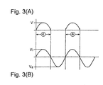
- Figs. 3(A) and 3(B) are diagrams of waveforms output by the second switching circuit and the dynamo, respectively.
-
- Fig. 1 is a conceptual schematic diagram of a particular embodiment of a battery charging and speed indicating circuit according to the present invention. The circuit comprises a dynamo 1 (generator), a first rectifying circuit 2 (first switching circuit), a second rectifying circuit 6 (second switching circuit), a secondary battery 3 (e.g., a capacitor) as a power supply for electrically driven units, and a switch 5 (third switching circuit) disposed between the
dynamo 1 and thesecondary battery 3. The circuit further comprises and a Schmittcircuit 7 coupled to the second rectifyingcircuit 6 for waveform shaping. - The
dynamo 1 may, for example, be a hub dynamo built into the hub of the bicycle front wheel, and it is provided with an internal impedance R and an internal inductance L. The rectifyingcircuit 2 contains diodes or the like to rectify the alternating-current voltage output by thedynamo 1 and to provide thesecondary battery 3 with the resulting positive or negative (e.g., positive) half-periods. Theswitch 5 contains capacitors, transistors or the like for selectively inhibiting the communication of the signals from rectifyingcircuit 2 tobattery 3. The second rectifyingcircuit 6 contains diodes or the like to rectify the alternating-current voltage output by thedynamo 1 and to provide the speedometer circuit (not shown) with the resulting positive or negative (e.g., negative) half-periods as a speed detection signal. The Schmittcircuit 7 receives the output of the second rectifyingcircuit 6 and outputs a pulse signal such as the one shown in Fig. 1 to facilitate the operation of the speedometer, which usually comprises a microcomputer. - The signal waveforms of the various components of the circuit shown in Fig. 1 will now be described. The
switch 5 is open or closed in accordance with the charging voltage of thesecondary battery 3. The switching operation causes the load resistance to change abruptly, thus markedly varying the voltage drop due to the effect of the internal impedance R or internal inductance L of thedynamo 1. The dynamo output waveform is thereby disrupted violently as shown in Fig. 1. In this case, the output waveform is disrupted only during the positive half-periods because charging occurs only during these half-periods. In conventional devices a low-pass filter or other circuit is needed to derive a speed detection signal from such a disrupted output waveform. In view of this, the present embodiment is configured such that the second rectifyingcircuit 6 retrieves the negative half-periods of the output provided by thedynamo 1, and the signal waveform is shaped to provide a pulse signal for speed detection. As shown in Fig. 1, the speed detection signal can be readily formed without waveform disruption. - Fig. 2 is a detailed schematic diagram of the circuit shown in Fig. 1. In the circuit shown in Fig. 2, the positive and negative parts of the waveforms output by the
dynamo 1 are the opposite of those produced by the circuit shown in Fig. 1. - As shown in Fig. 2,
dynamo 1 is coupled with a first capacitor C1, a second capacitor C2, a first diode D1, and a second diode D2. In this circuit, the first and second capacitors C1, C2 and the first and second diodes D1, D2 constitute a voltage-doubling rectifier circuit. The first capacitor C1 is charged during the positive half-cycle ofdynamo 1 output, and during the subsequent negative half-cycle the second capacitor C2 is charged with voltage equal to the voltage generated bydynamo 1 plus the charged voltage of the first capacitor C1. Thus, the second capacitor C2 can acquire high charged voltage at low speed. The second capacitor C2 functions as a power supply for driving first and third field-effect transistors FET1 and FET3, described later. - A third diode D3 serving as a rectifier circuit is coupled with
dynamo 1, and the output of this third diode D3 is coupled, via the first field-effect transistor (hereinafter simply "transistor") FET1, to a third capacitor C3 serving as a rechargeable battery. The gate of first transistor FET1 is coupled, via a first resistor R1, to the second capacitor C2. In this circuit, the third diode D3 allows the third capacitor C3 to be charged, via first transistor FET1, with the output ofdynamo 1 only during the negative half-cycle thereof. As is well known for such transistors, if the potential at the gate of first transistor FET1 is higher than that at the source by more than a predetermined level (2 V, for example), first transistor FET1 switches on. Since the voltage of the second capacitor C2 is applied to the gate of the first transistor FET1, the applied voltage is sufficiently high even under the low speed condition described earlier, the first transistor FET1 is stabilized in the ON state, and the third capacitor C3 charging operation is stabilized. - The second transistor FET2, third transistor FET3 (corresponding to
switch 5 in Fig. 1) andlamp 4 are connected in series todynamo 1. Diode D5, shown connected in parallel with second transistor FET2, and diode D4, shown connected in parallel with third transistor FET3, are parasitic diodes for the respective transistors FET2, FET3. The gate of the second transistor FET2 is coupled via a second resistor R2 to the second capacitor C2, and the gate of the third transistor FET3 is coupled to acontrol circuit 10. A third resistor R3 is also connected in parallel with the gate of third transistor FET3. - With this circuit arrangement, the gate potential of the first transistor FET1 can be controlled by
control circuit 10 to control charging of the third capacitor C3, and the gate potential of the third transistor FET3 can be controlled according to the charged voltage of the third capacitor C3 to control on/off operation of the third transistor FET3. By switching off the second transistor FET2 together with the third transistor FET3, thelamp 4 can be extinguished completely. - Diode D6 is connected to the output of
dynamo 1 to rectify the alternating-current voltage output by thedynamo 1 and to output the positive half-periods of the dynamo signals. The Schmittcircuit 7 receives the output of diode D6 and outputs a pulse signal such as the one shown in Fig. 1 as a speed detection signal to facilitate the operation of the speedometer, which usually comprises a microcomputer (not shown). Thus, the speed detection signal is produced from the positive half-periods of the generator output. - The operation of the circuit will now be described. It is assumed that all capacitors are initially empty. First, during the positive half-cycle of the output of
dynamo 1, current flows over path (1) :
(1): dynamo D1 C1 dynamo - This results in charging the first capacitor C1. The voltage across the first capacitor C1 reaches approximately the dynamo output peak voltage of 0.6 V.
- During the subsequent negative half-cycle current flows in reverse over path (2) :
(2): dynamo C1 D2 C2 D5 dynamo - This results in charging the second capacitor C2. The current supplied to the second capacitor C2 is equal to the current from
dynamo 1 plus current from the charged first capacitor C1. Thus, the second capacitor C2 can be charged adequately even at low speed. When the voltage across the second capacitor C2 reaches {(voltage across C3) + (ON trigger voltage for gate of FET1)}, the first transistor FET1 turns on. The second transistor FET2 turns on as well. Thus, current now flows also over path (3):
(3): dynamo D3 FET1 C3 FET2 dynamo - This initiates charging of the third capacitor C3.
With this arrangement, the third capacitor C3 can be stably charged to relatively high voltage during the negative half-cycle of dynamo output only. Furthermore, as the voltage applied to the gate of the first transistor FET1 can be stabilized by the second capacitor C2, the ON state of the first transistor FET1 can be stabilized. - At this time the voltage across the third capacitor C3 is not adequate for driving other electrically powered units in a stable manner. Thus, the voltage applied to the gate of the third transistor FET3 is controlled by the
control circuit 10 so that the third transistor FET3 remains off. During the positive half-cycle, the first capacitor C1 is charged by means of current flowing over path (1) :
(1) : dynamo D1 C1 dynamo
as described above, and thelamp 4 is lit by means of current flowing over path (4) :
(4) : dynamo FET2 D4 lamp dynamo. - During the subsequent negative half-cycle, the second capacitor C2 and third capacitor C3 are charged by means of current flowing over path (2) :
(2): dynamo C1 D2 C2 FET2 dynamo
and current flowing over path (3) :
(3): dynamo D3 FET1 C3 FET2 dynamo. - The above operation by means of current flowing over paths (1) and (4) during the positive half-cycle of dynamo output and operation by means of current flowing over paths (2) and (3) during the negative half-cycle, are performed repeatedly.
- When electric current flows along paths (1) and (4), the dynamo output of positive half-periods is extracted by the diode D6, and the waveform is shaped by the
Schmitt circuit 7. The pulse signal generated by theSchmitt circuit 7 is used as a speed detection signal. During positive half-periods, the load varies only slightly because it consists of thelamp 4 alone. Thus, a speed detection signal can be provided during those positive half-periods in a simple and accurate manner. - Fig. 3(b) shows the waveform of dynamo output in this case, and Fig. 3(a) shows the waveform of the diode D6 (which is also the waveform of the voltage applied to the lamp 4). As will be apparent from the drawings, the
lamp 4 is lit during the positive half-cycle of dynamo output, while the rechargeable battery (capacitor C3) is charged during the negative half-cycle. In Fig. 3(b), the positive peak voltage V1 is lower than the negative peak voltage V2; this is due to a drop in voltage in the dynamo resulting from the lamp load. The third capacitor C3 is repeatedly recharged in this manner, and when the voltage across the third capacitor C3 reaches a level sufficient to drive other devices, the third transistor FET3 is turned on by thecontrol circuit 10. This causes current to flow over path(5);
(5) dynamo lamp FET3 FET2 dynamo
so that the lamp lights. In this state the lamp is lit not intermittently, but continuously during both the positive and negative half-cycles of dynamo output. Thelamp 4 can be extinguished completely by switching off the second transistor FET2 in addition to the third transistor FET3. - While the above is a description of various embodiments of the present invention, further modifications may be employed without departing from the spirit and scope of the present invention. For example, the size, shape, location or orientation of the various components may be changed as desired. Components that are shown directly connected or contacting each other may have intermediate structures disposed between them. The functions of one element may be performed by two, and vice versa. It is not necessary for all advantages to be present in a particular embodiment at the same time. Every feature which is unique from the prior art, alone or in combination with other features, also should be considered a separate description of further inventions by the applicant, including the structural and/or functional concepts embodied by such feature(s). Thus, the scope of the invention should not be limited by the specific structures disclosed or the apparent initial focus on a particular structure or feature.
Claims (8)
- A circuit that receives signals from a dynamo (1) and provides signals for charging a battery (3) and indicating bicycle speed, wherein the circuit comprises:a first switching circuit (2) adapted to receive the dynamo signals and provide first signals for charging the battery (3); anda second switching circuit (6) adapted to receive the dynamo signals and provide second signals for indicating bicycle speed.
- The circuit according to claim 1 further comprising a pulse signal circuit (7) for providing pulse signals from the second signals.
- The circuit according to claim 2 wherein the pulse signal circuit (7) comprises a Schmitt circuit (7).
- The circuit according to any preceding claim further comprising a third switching circuit (5) that selectively inhibits the output of the first signals to the battery (3).
- The circuit according to claim 4 wherein the third switching circuit (5) comprises a transistor (FET3).
- The circuit according to any preceding claim wherein the first switching circuit (2) comprises a first diode element (D2), and wherein the second switching circuit (6) comprises a second diode element (D3).
- The circuit according to any preceding claim wherein the dynamo signals are periodic signals, wherein the first signals correspond to one of the half periods of the periodic signals, and wherein the second signals correspond to the other half periods of the periodic signals.
- The circuit according to claim 7 wherein the first signals correspond to positive half periods of the periodic signals, and wherein the second signals correspond to negative half periods of the periodic signals.
Priority Applications (1)
| Application Number | Priority Date | Filing Date | Title |
|---|---|---|---|
| EP04004052A EP1422805A3 (en) | 2001-03-22 | 2002-03-20 | Bicycle battery charger and speedometer circuit |
Applications Claiming Priority (2)
| Application Number | Priority Date | Filing Date | Title |
|---|---|---|---|
| JP2001083066A JP2002281691A (en) | 2001-03-22 | 2001-03-22 | Circuit for charging bicycle and detecting its speed |
| JP2001083066 | 2001-03-22 |
Related Child Applications (2)
| Application Number | Title | Priority Date | Filing Date |
|---|---|---|---|
| EP04004052A Division EP1422805A3 (en) | 2001-03-22 | 2002-03-20 | Bicycle battery charger and speedometer circuit |
| EP04004052.9 Division-Into | 2004-02-23 |
Publications (3)
| Publication Number | Publication Date |
|---|---|
| EP1244192A2 true EP1244192A2 (en) | 2002-09-25 |
| EP1244192A3 EP1244192A3 (en) | 2003-08-06 |
| EP1244192B1 EP1244192B1 (en) | 2012-05-09 |
Family
ID=18938932
Family Applications (2)
| Application Number | Title | Priority Date | Filing Date |
|---|---|---|---|
| EP04004052A Withdrawn EP1422805A3 (en) | 2001-03-22 | 2002-03-20 | Bicycle battery charger and speedometer circuit |
| EP02251979A Expired - Fee Related EP1244192B1 (en) | 2001-03-22 | 2002-03-20 | Bicycle battery charger and speedometer circuit |
Family Applications Before (1)
| Application Number | Title | Priority Date | Filing Date |
|---|---|---|---|
| EP04004052A Withdrawn EP1422805A3 (en) | 2001-03-22 | 2002-03-20 | Bicycle battery charger and speedometer circuit |
Country Status (6)
| Country | Link |
|---|---|
| US (2) | US6573686B2 (en) |
| EP (2) | EP1422805A3 (en) |
| JP (1) | JP2002281691A (en) |
| CN (1) | CN1251916C (en) |
| CZ (1) | CZ20021001A3 (en) |
| TW (1) | TW583109B (en) |
Cited By (4)
| Publication number | Priority date | Publication date | Assignee | Title |
|---|---|---|---|---|
| EP1391375A1 (en) * | 2002-08-20 | 2004-02-25 | Shimano Inc. | Power stabilizing apparatus for a bicycle electrical component |
| EP1488991A2 (en) * | 2003-06-18 | 2004-12-22 | Busch & Müller KG | Circuit for the brake dependent control of a bicycle lighting unit and a method therefor |
| EP1882999A3 (en) * | 2006-07-24 | 2011-07-27 | CAMPAGNOLO S.r.l. | Method and system for recharging a battery power supply unit |
| EP1465317B1 (en) * | 2003-04-01 | 2014-03-26 | Shimano Inc. | Bicycle power supply with reduced battery leakage |
Families Citing this family (13)
| Publication number | Priority date | Publication date | Assignee | Title |
|---|---|---|---|---|
| JP2002262473A (en) * | 2001-02-28 | 2002-09-13 | Shimano Inc | Charging control circuit for bicycle |
| JP3727315B2 (en) * | 2003-04-01 | 2005-12-14 | 株式会社シマノ | Bicycle power supply |
| JP3845092B2 (en) * | 2004-01-16 | 2006-11-15 | 株式会社シマノ | Bicycle lighting device |
| JP2008278614A (en) * | 2007-04-27 | 2008-11-13 | Shimano Inc | Power supply device and electric system for bicycle |
| US8307967B2 (en) | 2007-07-04 | 2012-11-13 | Satyajit Patwardhan | Widely deployable charging system for vehicles |
| TWM411566U (en) | 2010-11-01 | 2011-09-11 | Shimano Kk | Wheel hub used for bicycle and rotation status detection apparatus used for bicycle |
| US10059254B2 (en) * | 2011-12-20 | 2018-08-28 | Ethan Perry Frier | Communicating information regarding status of vehicle operation |
| US9018940B2 (en) | 2012-06-28 | 2015-04-28 | Shimano Inc. | Bicycle rotation detecting device |
| KR20140038049A (en) * | 2012-09-19 | 2014-03-28 | 주식회사 만도 | Eletric bicycle and control method thereof |
| KR101532776B1 (en) * | 2013-11-26 | 2015-06-30 | 주식회사 만도 | Chainless eletric bicycle |
| CN105242062B (en) * | 2015-10-10 | 2019-11-26 | 广东威创视讯科技股份有限公司 | Fan rotation-speed detection device |
| JP6767667B2 (en) * | 2016-03-07 | 2020-10-14 | パナソニックIpマネジメント株式会社 | Bicycle rear alarm device |
| WO2018058504A1 (en) * | 2016-09-30 | 2018-04-05 | 深圳博芯科技股份有限公司 | 2.4ghz wireless code table circuit |
Citations (4)
| Publication number | Priority date | Publication date | Assignee | Title |
|---|---|---|---|---|
| US3731533A (en) * | 1969-10-16 | 1973-05-08 | Dresser Ind | Electrical generator having non-salient poles for metering shaft rotation of a turbine assembly |
| US3875421A (en) * | 1973-05-14 | 1975-04-01 | Needs Inc | Bicycle light system |
| WO1981001274A1 (en) * | 1979-11-06 | 1981-05-14 | T Murphy | Bicycle or other vehicle generator improvement unit |
| EP0645868A2 (en) * | 1993-09-24 | 1995-03-29 | Casio Computer Co., Ltd. | Charging apparatus |
Family Cites Families (7)
| Publication number | Priority date | Publication date | Assignee | Title |
|---|---|---|---|---|
| US4197585A (en) * | 1978-03-02 | 1980-04-08 | Mckendrick Jeremy D | Vehicle speed measuring apparatus |
| DE4232182A1 (en) | 1992-09-25 | 1994-03-31 | Wilfried Schmidt | Hub generator, in particular for bicycles |
| JPH07229909A (en) | 1994-02-17 | 1995-08-29 | Sanyo Electric Co Ltd | Bicycle speedometer |
| AU5544296A (en) * | 1995-04-11 | 1996-10-30 | Aerovironment Inc. | Electric power apparatus for a wheeled vehicle |
| JPH08337192A (en) | 1995-06-14 | 1996-12-24 | Matsushita Electric Ind Co Ltd | Motor assisted bicycle |
| US6290014B1 (en) * | 1999-02-09 | 2001-09-18 | Maccready, Jr. Paul B. | Power assist for bicycles |
| JP3573723B2 (en) * | 2001-06-29 | 2004-10-06 | 株式会社シマノ | Gear change control device for bicycle |
-
2001
- 2001-03-22 JP JP2001083066A patent/JP2002281691A/en active Pending
-
2002
- 2002-01-16 TW TW091100617A patent/TW583109B/en not_active IP Right Cessation
- 2002-03-18 US US10/100,936 patent/US6573686B2/en not_active Ceased
- 2002-03-20 EP EP04004052A patent/EP1422805A3/en not_active Withdrawn
- 2002-03-20 EP EP02251979A patent/EP1244192B1/en not_active Expired - Fee Related
- 2002-03-20 CZ CZ20021001A patent/CZ20021001A3/en unknown
- 2002-03-21 CN CN02107811.4A patent/CN1251916C/en not_active Expired - Fee Related
-
2004
- 2004-01-30 US US10/769,727 patent/USRE41015E1/en not_active Expired - Lifetime
Patent Citations (4)
| Publication number | Priority date | Publication date | Assignee | Title |
|---|---|---|---|---|
| US3731533A (en) * | 1969-10-16 | 1973-05-08 | Dresser Ind | Electrical generator having non-salient poles for metering shaft rotation of a turbine assembly |
| US3875421A (en) * | 1973-05-14 | 1975-04-01 | Needs Inc | Bicycle light system |
| WO1981001274A1 (en) * | 1979-11-06 | 1981-05-14 | T Murphy | Bicycle or other vehicle generator improvement unit |
| EP0645868A2 (en) * | 1993-09-24 | 1995-03-29 | Casio Computer Co., Ltd. | Charging apparatus |
Cited By (6)
| Publication number | Priority date | Publication date | Assignee | Title |
|---|---|---|---|---|
| EP1391375A1 (en) * | 2002-08-20 | 2004-02-25 | Shimano Inc. | Power stabilizing apparatus for a bicycle electrical component |
| EP1465317B1 (en) * | 2003-04-01 | 2014-03-26 | Shimano Inc. | Bicycle power supply with reduced battery leakage |
| EP1488991A2 (en) * | 2003-06-18 | 2004-12-22 | Busch & Müller KG | Circuit for the brake dependent control of a bicycle lighting unit and a method therefor |
| EP1488991A3 (en) * | 2003-06-18 | 2005-10-05 | Busch & Müller KG | Circuit for the brake dependent control of a bicycle lighting unit and a method therefor |
| EP1882999A3 (en) * | 2006-07-24 | 2011-07-27 | CAMPAGNOLO S.r.l. | Method and system for recharging a battery power supply unit |
| US8143849B2 (en) | 2006-07-24 | 2012-03-27 | Campagnolo S.R.L. | Method and system for recharging a battery power supply unit for a bicycle electronic device |
Also Published As
| Publication number | Publication date |
|---|---|
| CZ20021001A3 (en) | 2003-08-13 |
| US6573686B2 (en) | 2003-06-03 |
| JP2002281691A (en) | 2002-09-27 |
| CN1376604A (en) | 2002-10-30 |
| US20020135337A1 (en) | 2002-09-26 |
| EP1422805A3 (en) | 2004-06-02 |
| EP1422805A2 (en) | 2004-05-26 |
| USRE41015E1 (en) | 2009-12-01 |
| CN1251916C (en) | 2006-04-19 |
| TW583109B (en) | 2004-04-11 |
| EP1244192B1 (en) | 2012-05-09 |
| EP1244192A3 (en) | 2003-08-06 |
Similar Documents
| Publication | Publication Date | Title |
|---|---|---|
| EP1244192B1 (en) | Bicycle battery charger and speedometer circuit | |
| US6323623B1 (en) | Charging device and charging method thereof | |
| TW553865B (en) | Power source device for bicycle | |
| CN100411274C (en) | DC power supply device for human powered vehicles | |
| US3904920A (en) | Safety lighting system | |
| TWI246979B (en) | Power supply device for bicycle and power supply method for bicycle | |
| SI1601078T1 (en) | Power mos voltage regulator for batteries | |
| TWI284608B (en) | Charging control circuit for bicycle | |
| JP3645881B2 (en) | Bicycle dynamo charger | |
| JPH07111735A (en) | Auxiliary unit battery charging system for electric motor vehicle | |
| US20040051506A1 (en) | Bicycle power supply with full-wave and half-wave charging elements | |
| ATE158722T1 (en) | POWER SUPPLY DEVICE FOR AN EXERCISE BIKE | |
| JP2000062523A (en) | Illumination lighting control device for bicycle | |
| WO2020065767A1 (en) | Charging coil unit, power unit, and work machine | |
| KR0164480B1 (en) | Charging control apparatus of electric vehicle | |
| JP5921903B2 (en) | Power generation control device and transportation equipment | |
| KR200316732Y1 (en) | Voltage regulator of car generator | |
| JPS6334439Y2 (en) | ||
| JP2771596B2 (en) | Inverter | |
| WO2020065768A1 (en) | Control device, battery unit, and work machine | |
| KR200237623Y1 (en) | Apparatus for battery charge | |
| JPH07325983A (en) | Blinking display device | |
| KR20060023838A (en) | A rechargeable battery recharger with a reserve rechargeable battery | |
| JP2003111420A (en) | Ac voltage regulator and charger | |
| JPH037624U (en) |
Legal Events
| Date | Code | Title | Description |
|---|---|---|---|
| PUAI | Public reference made under article 153(3) epc to a published international application that has entered the european phase |
Free format text: ORIGINAL CODE: 0009012 |
|
| AK | Designated contracting states |
Kind code of ref document: A2 Designated state(s): AT BE CH CY DE DK ES FI FR GB GR IE IT LI LU MC NL PT SE TR |
|
| AX | Request for extension of the european patent |
Free format text: AL;LT;LV;MK;RO;SI |
|
| PUAL | Search report despatched |
Free format text: ORIGINAL CODE: 0009013 |
|
| AK | Designated contracting states |
Designated state(s): AT BE CH CY DE DK ES FI FR GB GR IE IT LI LU MC NL PT SE TR |
|
| AX | Request for extension of the european patent |
Extension state: AL LT LV MK RO SI |
|
| 17P | Request for examination filed |
Effective date: 20030826 |
|
| 17Q | First examination report despatched |
Effective date: 20031023 |
|
| AKX | Designation fees paid |
Designated state(s): DE FR GB IE IT NL |
|
| RAP1 | Party data changed (applicant data changed or rights of an application transferred) |
Owner name: SHIMANO INC. |
|
| GRAP | Despatch of communication of intention to grant a patent |
Free format text: ORIGINAL CODE: EPIDOSNIGR1 |
|
| GRAS | Grant fee paid |
Free format text: ORIGINAL CODE: EPIDOSNIGR3 |
|
| GRAA | (expected) grant |
Free format text: ORIGINAL CODE: 0009210 |
|
| AK | Designated contracting states |
Kind code of ref document: B1 Designated state(s): DE FR GB IE IT NL |
|
| REG | Reference to a national code |
Ref country code: GB Ref legal event code: FG4D |
|
| REG | Reference to a national code |
Ref country code: IE Ref legal event code: FG4D |
|
| REG | Reference to a national code |
Ref country code: DE Ref legal event code: R096 Ref document number: 60242852 Country of ref document: DE Effective date: 20120712 |
|
| REG | Reference to a national code |
Ref country code: NL Ref legal event code: T3 |
|
| PG25 | Lapsed in a contracting state [announced via postgrant information from national office to epo] |
Ref country code: IT Free format text: LAPSE BECAUSE OF FAILURE TO SUBMIT A TRANSLATION OF THE DESCRIPTION OR TO PAY THE FEE WITHIN THE PRESCRIBED TIME-LIMIT Effective date: 20120509 |
|
| PLBE | No opposition filed within time limit |
Free format text: ORIGINAL CODE: 0009261 |
|
| STAA | Information on the status of an ep patent application or granted ep patent |
Free format text: STATUS: NO OPPOSITION FILED WITHIN TIME LIMIT |
|
| 26N | No opposition filed |
Effective date: 20130212 |
|
| REG | Reference to a national code |
Ref country code: DE Ref legal event code: R097 Ref document number: 60242852 Country of ref document: DE Effective date: 20130212 |
|
| GBPC | Gb: european patent ceased through non-payment of renewal fee |
Effective date: 20130320 |
|
| REG | Reference to a national code |
Ref country code: FR Ref legal event code: ST Effective date: 20131129 |
|
| REG | Reference to a national code |
Ref country code: IE Ref legal event code: MM4A |
|
| PG25 | Lapsed in a contracting state [announced via postgrant information from national office to epo] |
Ref country code: IE Free format text: LAPSE BECAUSE OF NON-PAYMENT OF DUE FEES Effective date: 20130320 Ref country code: GB Free format text: LAPSE BECAUSE OF NON-PAYMENT OF DUE FEES Effective date: 20130320 Ref country code: FR Free format text: LAPSE BECAUSE OF NON-PAYMENT OF DUE FEES Effective date: 20130402 |
|
| PGFP | Annual fee paid to national office [announced via postgrant information from national office to epo] |
Ref country code: NL Payment date: 20160210 Year of fee payment: 15 |
|
| REG | Reference to a national code |
Ref country code: NL Ref legal event code: MM Effective date: 20170401 |
|
| PG25 | Lapsed in a contracting state [announced via postgrant information from national office to epo] |
Ref country code: NL Free format text: LAPSE BECAUSE OF NON-PAYMENT OF DUE FEES Effective date: 20170401 |
|
| PGFP | Annual fee paid to national office [announced via postgrant information from national office to epo] |
Ref country code: DE Payment date: 20180306 Year of fee payment: 17 |
|
| REG | Reference to a national code |
Ref country code: DE Ref legal event code: R119 Ref document number: 60242852 Country of ref document: DE |
|
| PG25 | Lapsed in a contracting state [announced via postgrant information from national office to epo] |
Ref country code: DE Free format text: LAPSE BECAUSE OF NON-PAYMENT OF DUE FEES Effective date: 20191001 |