EP1244007A2 - Dynamische Mikrokodemodifikation - Google Patents
Dynamische Mikrokodemodifikation Download PDFInfo
- Publication number
- EP1244007A2 EP1244007A2 EP02090117A EP02090117A EP1244007A2 EP 1244007 A2 EP1244007 A2 EP 1244007A2 EP 02090117 A EP02090117 A EP 02090117A EP 02090117 A EP02090117 A EP 02090117A EP 1244007 A2 EP1244007 A2 EP 1244007A2
- Authority
- EP
- European Patent Office
- Prior art keywords
- ram
- microcode
- rom
- address
- memory
- Prior art date
- Legal status (The legal status is an assumption and is not a legal conclusion. Google has not performed a legal analysis and makes no representation as to the accuracy of the status listed.)
- Ceased
Links
Images


Classifications
-
- G—PHYSICS
- G06—COMPUTING OR CALCULATING; COUNTING
- G06F—ELECTRIC DIGITAL DATA PROCESSING
- G06F9/00—Arrangements for program control, e.g. control units
- G06F9/06—Arrangements for program control, e.g. control units using stored programs, i.e. using an internal store of processing equipment to receive or retain programs
- G06F9/22—Microcontrol or microprogram arrangements
- G06F9/26—Address formation of the next micro-instruction ; Microprogram storage or retrieval arrangements
- G06F9/262—Arrangements for next microinstruction selection
- G06F9/268—Microinstruction selection not based on processing results, e.g. interrupt, patch, first cycle store, diagnostic programs
-
- G—PHYSICS
- G06—COMPUTING OR CALCULATING; COUNTING
- G06F—ELECTRIC DIGITAL DATA PROCESSING
- G06F8/00—Arrangements for software engineering
- G06F8/60—Software deployment
- G06F8/65—Updates
- G06F8/66—Updates of program code stored in read-only memory [ROM]
-
- G—PHYSICS
- G06—COMPUTING OR CALCULATING; COUNTING
- G06F—ELECTRIC DIGITAL DATA PROCESSING
- G06F9/00—Arrangements for program control, e.g. control units
- G06F9/06—Arrangements for program control, e.g. control units using stored programs, i.e. using an internal store of processing equipment to receive or retain programs
- G06F9/22—Microcontrol or microprogram arrangements
- G06F9/26—Address formation of the next micro-instruction ; Microprogram storage or retrieval arrangements
- G06F9/262—Arrangements for next microinstruction selection
- G06F9/264—Microinstruction selection based on results of processing
- G06F9/267—Microinstruction selection based on results of processing by instruction selection on output of storage
-
- G—PHYSICS
- G06—COMPUTING OR CALCULATING; COUNTING
- G06F—ELECTRIC DIGITAL DATA PROCESSING
- G06F9/00—Arrangements for program control, e.g. control units
- G06F9/06—Arrangements for program control, e.g. control units using stored programs, i.e. using an internal store of processing equipment to receive or retain programs
- G06F9/30—Arrangements for executing machine instructions, e.g. instruction decode
- G06F9/32—Address formation of the next instruction, e.g. by incrementing the instruction counter
- G06F9/322—Address formation of the next instruction, e.g. by incrementing the instruction counter for non-sequential address
- G06F9/328—Address formation of the next instruction, e.g. by incrementing the instruction counter for non-sequential address for runtime instruction patching
Definitions
- This disclosure relates to microprocessor system architecture, and more particularly to a microprocessor architecture that allows read-only memory (ROM) microcode to be effectively altered or enhanced without the need to reprogram or replace the ROM.
- ROM read-only memory
- a microprocessor is a central processing unit (CPU) enclosed in one integrated circuit (IC) package. Because of their small size and low cost, microprocessors have revolutionized digital system design technology, giving the designer the capability to create structures that were previously uneconomical. Microprocessors are used in a wide variety of applications. They can function as a CPU in a general purpose computer or as a processor unit in a special purpose, automated system.
- Microprocessor systems usually incorporate several different types of memory devices to hold data for processing and instructions for system control.
- Memory devices come in a wide variety of forms. Two of the more common forms are generally referred to as “read-only memory” (ROM) and “random access memory” (RAM).
- ROM read-only memory
- RAM random access memory
- ROM memory device In its simplest form, sometimes called “mask-programmed", a ROM memory device is manufactured with fixed contents. The binary information stored in the ROM is made permanent during the hardware production of the unit and cannot subsequently be altered. Such a ROM memory unit allows the read operation only; it does not have a write capability.
- ROM is most often used to hold microcode, the lowest level instructions that directly control a microprocessor and immutable data such as tables of constants.
- microcode can refer both to microprocessor instructions and immutable data programmed into ROM.
- a RAM is a data storage device that allows both the read and write function.
- a system CPU uses its RAM as a storage area for data, calculation results, and program instructions, drawing on this storage as necessary to perform the tasks required by programs. Its binary contents can easily be changed during operation and its stored data is typically erased or lost when the device incorporating it is powered off.
- Part of the initial "power-up" or boot routine for microprocessor systems includes the loading of desired or necessary code into RAM according to the system design.
- Microprocessor systems may also incorporate some type of "non-volatile" memory, such as a hard-disk. Like RAM, such memory can usually be read or written to, but unlike RAM its content is preserved until over-written, even without system power.
- non-volatile memory such as a hard-disk.
- PROM programmable read-only memory
- EPROM erasable programmable read-only memory
- EEPROM electroly erasable read-only memory
- PROM can only be programmed once and EPROM must be removed from the system to be reprogrammed.
- EEPROM must be erased and reprogrammed in its entirety, not selectively. For many processing systems, especially those used to perform set, repetitive tasks, it is desirable to use the cheapest and simplest ROM, usually of the "mask programmed" variety, with minimal reliance on more expensive RAM or other types of memory devices.
- a microprocessor system architecture allows for the selective execution of programmed ROM microcode or, alternatively, RAM microcode if there has been a correction or update made to the ROM microcode originally programmed into the system. Patched or updated RAM microcode is utilized or executed only to the extent of changes to the ROM microcode, otherwise the ROM microcode is executed in its normal fashion.
- the term "patch” is intended to mean any correction, change, or alteration to the original microcode stored in a microprocessor system's read-only memory (ROM).
- ROM read-only memory
- the terms “patch” or “update” may also be used herein to refer to microcode developed after the original programming of system ROM microcode for the implementation of new instructions or routines.
- microcode is intended to refer to the programmed contents of ROM, including the lowest level instructions that directly control a microprocessor and fixed data such as tables of constants.
- the system disclosed herein effectively allows for changes in otherwise unalterable ROM microcode, by loading microcode changes into a minimal amount of associated RAM and then providing for the selective execution of the existing ROM microcode or the changed RAM microcode.
- the disclosed techniques can be applied to any microprocessor system, but will be most beneficial for those systems that for economic or other reasons primarily rely on ROM memory devices that are programmed at system manufacture and incapable of alteration once programmed.
- Patch or updated microcode can be received and taken into the system in the same manner as other forms of data by, for example, modem, wireless data link, disk, or CD. Once received, the patch may be stored in any non-volatile memory device accessible by the system, where it will be available for subsequent loading into the associated RAM. Alternatively, when initially received from an external source, the patch microcode may be simultaneously loaded into RAM (for immediate use) and into available non-volatile memory for more permanent storage and future access.
- a microprocessor system's architecture is closely related to the organization of its memory. The amount of memory needed to perform the desired function(s), the type of memory to be used, and the organization of that memory must be considered by the system designer, along with other factors such as cost and size.
- each address of at least one portion of the designated RAM address area(s) will contain one or more control or "select" bits to signal a change to existing ROM microcode.
- select bit when the select bit is detected, the system is directed to execute the changed RAM microcode rather than existing ROM microcode.
- Figures 1A and 1B illustrate a memory architecture in which each pre-assigned block of ROM microcode 101A, 101B in the alternative embodiments has a corresponding block of RAM 103A, 103B. It is to be understood that the blocks of Figures 1A, 1B are merely representative of conventional memory circuitry present in or associated with a microprocessor including the arrays of memory cells, addressing and control circuitry, and other conventional memory elements. Each ROM memory space consists of n bits, whereas the corresponding RAM memory address space consists of n + 1 bits. The extra RAM bit 102A, 102B in each memory word may be referred to as a "select bit".
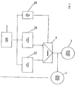
- Figure 2 illustrates one method for implementing the memory architecture shown in Figures 1A and 1B.
- the program counter 201 or other control unit conventionally present in a microprocessor simultaneously addresses main ROM 101A, 101B, main RAM 103A, 103B, and the RAM select bit 102A, 102B.
- the ROM microcode and RAM microcode instructions held in the respective memory at the selected address are input to a conventional circuit multiplexer 202.
- the RAM select bit is input to the select terminal of the multiplexer and used to control the selection of ROM microcode or RAM microcode as the output signal of the multiplexer.
- the multiplexer selects either the ROM microcode or the RAM microcode for output and further processing.
- the RAM microcode is selected, otherwise ROM microcode is selected.
- the microcode selected for output from the multiplexer is then executed through conventional microcode processing logic circuits 203 and the program counter 201 incremented or branched as necessary to initiate the next microcode instruction, again through conventional means 204.
- microprocessor programs frequently utilize conditional or branched sub-routines during their execution.
- the program may be directed to branch to a designated sub-routine and, once the sub-routine is completed, return to the main program instructions.
- these sub-routines will often include more microcode instructions and occupy more memory space than the main program instructions.
- Figure 3 illustrates a microprocessor memory architecture in which ROM microcode is programmed into two separate memory circuitss.
- main ROM 301 stores the basic program instructions while another circuit, denoted “routine” ROM 302 stores the microcode for the execution of sub-routines 1 through n as called for by the main program.
- routine ROM 302 stores the microcode for the execution of sub-routines 1 through n as called for by the main program.
- the address of sub-routine is sent to the program counter or similar conventional control unit.
- the address of sub-routine will include a bit, usually the most significant bit (MSB), to denote the circuit 301 or 302, containing the sub-routine microcode for execution.
- MSB most significant bit
- each n -bit block of routine ROM microcode shares the same address as an n + 1 bit block of RAM, where n is equal to the number of bits allocated to store each micro-code instruction. Any patches or changes to a routine ROM microcode are loaded into the corresponding (that is, same) address in RAM 304, along with an extra "select" bit 303 used to signal the existence of a change in the routine ROM microcode. This allows for the use of less RAM than that depicted in Figures 1A and 1B, although it is not possible to make changes to the main ROM microcode once it is programmed.
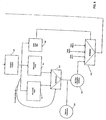
- Figure 4 illustrates a microprocessor system for implementing the memory architecture shown in Figure 3.
- the program counter 201 simultaneously addresses main ROM 301, routine ROM 302, routine RAM 304, and the RAM select bit 303.
- the routine ROM 302 and routine RAM 304 microcode are input to a multiplexer 401.
- the RAM select bit 303 applied to the control terminal of multiplexer 401 controls the selection of routine ROM microcode or routine RAM microcode as the output signal of the multiplexer.
- the multiplexer selects either the routine ROM microcode 302 or the routine RAM microcode 304 for output.
- the selected output from multiplexer 401 is input to another multiplexer 402.
- Main ROM microcode 301 is also input to multiplexer 402.
- the most significant bit (MSB) or other control bit 403 from the program counter 201 is used to select the output of multiplexer 402.
- MSB most significant bit
- main ROM microcode or the output of multiplexer 401 (routine ROM or routine RAM microcode) is selected for output and further processing.
- the microcode selected for output from multiplexer 402 is then executed by conventional means 203 and the program counter incremented or branched as required by conventional means 204 to initiate the next microcode instruction.
- FIGS 5A, 5B, and 5C illustrate a memory architecture in which ROM microcode is again segregated into separate circuits, one for "main” ROM microcode 501 and the other for "routine" ROM microcode 504.
- the main ROM address area 501 contains the basic program instructions while the routine ROM address area 504 contains the sub-routines that may be called for during the execution of the main program instructions.
- each pre-assigned n -bit block of ROM microcode 501 has a corresponding block of RAM 503 that is n + 1 bits wide.
- the extra RAM bit 502 may be referred to as a "select bit".
- main RAM 503 is allocated a larger memory space than main ROM 501 to allow for the implementation of new, not just altered program microcode, which can be stored in the additional RAM memory space.
- An additional RAM circuit, designated "routine" RAM 505, is incorporated to accept the loading of changes to the routine ROM microcode.
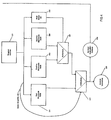
- Figure 6 illustrates a system for implementing the memory architecture shown in Figures 5A, 5B, and 5C.
- the program counter 201 simultaneously addresses main ROM 501, main RAM 503, routine ROM 504, routine RAM 505, and the RAM select bit 502.
- the addressed main ROM microcode and main RAM microcode are used as inputs to multiplexer 601.
- the RAM select bit 502 is applied to the control terminal of multiplexer 601 to control the output signal of the multiplexer, either main ROM microcode or main RAM microcode. This output is then directed to multiplexer 602.
- Routine ROM microcode 504 and routine RAM microcode 505 are also input to multiplexer 602.
- control bits 403 from the program counter 201 are applied to the multiplexer's select terminals since there are three possible outputs.
- control bits typically the two most significant bits, MSBs
- routine ROM microcode, routine RAM microcode, or the output of multiplexer 601 main ROM or main RAM microcode
- the microcode selected for output from multiplexer 602 is then executed 203 and the program counter incremented or branched as required 204 to initiate the next microcode instruction.
- FIGS. 7A, 7B, and 7C illustrate a memory architecture in which all ROM microcode is stored in the same address space. Any program reference to a specific ROM microcode address 701 will also reference the same address in a portion of RAM designated to hold one or more "valid" bits 702.
- the number of allocated valid bits, n depends upon the allowed or anticipated range of starting addresses, 2 n , of any microcode patches provided for. Each patch may consist of a single microcode instruction, or a sub-routine consisting of a number of instructions commenced from a given starting address and executed sequentially through a series of addresses.
- the valid bits will be set to denote the starting address of the patch instruction or routine.
- Figure 8 illustrates a system for implementing the memory architecture shown in Figures 7A, 7B, and 7C.
- the program counter 201 simultaneously addresses ROM 701, RAM 703, and the RAM valid bit(s) 702.
- the ROM 701 and RAM 703 are inputs to multiplexer 801.
- An MSB or other control bit 403 from the program counter is input to the select terminal of the multiplexer.
- the RAM or ROM microcode instruction is selected as the output signal of the multiplexer.
- the instruction is conventionally executed 203, and the address of the next instruction for execution is conventionally determined 204 and used as an input to a second multiplexer 802 rather than being sent to the program counter 201.
- the start address of any loaded patch instruction or routine (from RAM 703) are also input to multiplexer 802.
- the RAM valid bits are input to the select terminal of the multiplexer and used to select the address of the next instruction for execution by the program counter.
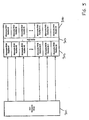
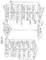
- Figures 9A through 9C illustrate a memory architecture in which a portion of system RAM (denoted "index" RAM), 902, is used to store the address location for each ROM microcode routine 903 or instruction.
- the addresses are loaded into index RAM when the system is initialized on startup, or when a patch to system ROM microcode is received.
- a microcode ROM 901 routine or instruction is to be executed, the system is directed to obtain the microcode address from index RAM, which can be done by well known programming techniques.
- Figure 9A if there has been no change or addition to the microcode, the system will be directed to a ROM address, whereupon it will execute the routine or instruction stored in ROM.
- FIG 9B illustrates how patch RAM routines in 904 are executed instead of ROM routines in 903.
- the patch RAM routines are installed in 904 and the index addresses in 902 are selectively changed, to point to the locations of the correct routines.
- the applicable RAM address will be submitted for the corresponding ROM instruction address and the routine executed in order from the patch RAM 904.
- Figure 9C illustrates the case when entirely new microcode has been received.
- the new instructions are loaded into main RAM 905 and the locations of the updated routines in patch RAM 904 are written to the index RAM 902.
- Figure 9C illustrates two key points.
- Figure 9C shows how the main microcode Ram 905 calls both ROM routines in 903 and patch RAM routines in 904 by selectively changing the index addresses in 902.
- Figure 9C shows how new updated RAM routines in 904 are executed by the main microcode RAM 905 by adding new entries to the previously unused space of the index address RAM 902 to point to the locations of the new routines.
- the Patch Microcode RAM Routine #p in 904 is an example of an updated RAM routine.
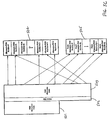
- Figure 10 illustrates a system for implementing the memory architecture shown in Figures 9A, 9B, and 9C.
- Program counter 201 simultaneously addresses routine ROM 903, main ROM 901, main RAM 905, and routine RAM 904.
- the address portion of the main RAM and main ROM microcode are used as inputs to multiplexer 1001.
- the most significant bit (MSB) 403 or other control bit from the program counter 201 is used to select the output of multiplexer 1001.
- MSB most significant bit
- main ROM microcode address or main RAM microcode address is selected for output from multiplexer 1001.
- the selected RAM or ROM address portion of the instruction is then conventionally mapped to its corresponding address in the index RAM 902.
- routine ROM microcode and routine RAM microcode are input to multiplexer 1002.
- MSB most significant bit
- routine ROM microcode, routine RAM microcode, main ROM or main RAM is selected for output and execution 203 and to set the address for the next instruction 204.
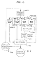
- FIG. 11 is a programming flow chart showing a microcode patch initialization routine for the memory architecture depicted in Figures 9A, 9B, and 9C.
- program initialization 1101 all index RAM locations are set to the unused pattern (such as all "1s") 1102.
- An index is read from ROM 1103 and written to RAM 1104, and pointer incremented to show the next index location 1105. The process is repeated until all indexes are initialized in order 1106.
- the presence of a microcode patch is queried from non-volatile memory used to store any patch routines by, for example, sampling the status of a designated "patch" bit 1107.
- the patch initialization routine is started 1108, its index is read from non-volatile memory 1109 and written to the corresponding RAM index location 1110.
- the patch routine is then read from non-volatile memory 1111 and written to the designated patch RAM area of memory 1112.
- the program pointer is incremented 1113 and the process repeated until all patches have been indexed and written to RAM 1114.
- the patch initialization program then returns to the main routine 1115.
Landscapes
- Engineering & Computer Science (AREA)
- Software Systems (AREA)
- Theoretical Computer Science (AREA)
- General Engineering & Computer Science (AREA)
- Physics & Mathematics (AREA)
- General Physics & Mathematics (AREA)
- Computer Security & Cryptography (AREA)
- Stored Programmes (AREA)
Applications Claiming Priority (2)
| Application Number | Priority Date | Filing Date | Title |
|---|---|---|---|
| US09/815,098 US6804772B2 (en) | 2000-06-12 | 2001-03-21 | Dynamic field patchable microarchitecture |
| US815098 | 2001-03-21 |
Publications (2)
| Publication Number | Publication Date |
|---|---|
| EP1244007A2 true EP1244007A2 (de) | 2002-09-25 |
| EP1244007A3 EP1244007A3 (de) | 2007-05-23 |
Family
ID=25216844
Family Applications (1)
| Application Number | Title | Priority Date | Filing Date |
|---|---|---|---|
| EP02090117A Ceased EP1244007A3 (de) | 2001-03-21 | 2002-03-21 | Dynamische Mikrokodemodifikation |
Country Status (1)
| Country | Link |
|---|---|
| EP (1) | EP1244007A3 (de) |
Cited By (3)
| Publication number | Priority date | Publication date | Assignee | Title |
|---|---|---|---|---|
| EP1507410A1 (de) * | 2003-08-14 | 2005-02-16 | Broadcom Corporation | Reprogrammierbarer Steuersignalgenerator für Videosignale |
| EP1507200A3 (de) * | 2003-08-11 | 2007-08-29 | Telairity Semiconductor, Inc. | System zur Reparatur von ROM Fehlern oder Programmierdefekten |
| US7489362B2 (en) | 2003-03-04 | 2009-02-10 | Broadcom Corporation | Television functionality on a chip |
Citations (4)
| Publication number | Priority date | Publication date | Assignee | Title |
|---|---|---|---|---|
| US3659257A (en) | 1968-11-04 | 1972-04-25 | Woods Hole Oceanographic Inst | Continuous magnetic line hydrophone |
| US3934227A (en) | 1973-12-05 | 1976-01-20 | Digital Computer Controls, Inc. | Memory correction system |
| WO1992008231A1 (en) | 1990-11-02 | 1992-05-14 | Transcomputer, Inc. | Rom patch device |
| US5757690A (en) | 1997-04-23 | 1998-05-26 | Exponential Technology, Inc. | Embedded ROM with RAM valid bits for fetching ROM-code updates from external memory |
Family Cites Families (4)
| Publication number | Priority date | Publication date | Assignee | Title |
|---|---|---|---|---|
| US3659275A (en) * | 1970-06-08 | 1972-04-25 | Cogar Corp | Memory correction redundancy system |
| DE2621399A1 (de) * | 1975-05-29 | 1976-12-09 | Int Standard Electric Corp | Speichereinrichtung |
| US4982360A (en) * | 1983-09-22 | 1991-01-01 | Digital Equipment Corporation | Memory subsystem |
| US6141740A (en) * | 1997-03-03 | 2000-10-31 | Advanced Micro Devices, Inc. | Apparatus and method for microcode patching for generating a next address |
-
2002
- 2002-03-21 EP EP02090117A patent/EP1244007A3/de not_active Ceased
Patent Citations (4)
| Publication number | Priority date | Publication date | Assignee | Title |
|---|---|---|---|---|
| US3659257A (en) | 1968-11-04 | 1972-04-25 | Woods Hole Oceanographic Inst | Continuous magnetic line hydrophone |
| US3934227A (en) | 1973-12-05 | 1976-01-20 | Digital Computer Controls, Inc. | Memory correction system |
| WO1992008231A1 (en) | 1990-11-02 | 1992-05-14 | Transcomputer, Inc. | Rom patch device |
| US5757690A (en) | 1997-04-23 | 1998-05-26 | Exponential Technology, Inc. | Embedded ROM with RAM valid bits for fetching ROM-code updates from external memory |
Non-Patent Citations (1)
| Title |
|---|
| IBM TECHNICAL DISCLOSURE BULLETIN, vol. 26, December 1983 (1983-12-01) |
Cited By (5)
| Publication number | Priority date | Publication date | Assignee | Title |
|---|---|---|---|---|
| US7489362B2 (en) | 2003-03-04 | 2009-02-10 | Broadcom Corporation | Television functionality on a chip |
| US7961255B2 (en) | 2003-03-04 | 2011-06-14 | Broadcom Corporation | Television functionality on a chip |
| US8854545B2 (en) | 2003-03-04 | 2014-10-07 | Broadcom Corporation | Television functionality on a chip |
| EP1507200A3 (de) * | 2003-08-11 | 2007-08-29 | Telairity Semiconductor, Inc. | System zur Reparatur von ROM Fehlern oder Programmierdefekten |
| EP1507410A1 (de) * | 2003-08-14 | 2005-02-16 | Broadcom Corporation | Reprogrammierbarer Steuersignalgenerator für Videosignale |
Also Published As
| Publication number | Publication date |
|---|---|
| EP1244007A3 (de) | 2007-05-23 |
Similar Documents
| Publication | Publication Date | Title |
|---|---|---|
| US6804772B2 (en) | Dynamic field patchable microarchitecture | |
| US6834384B2 (en) | Methods and apparatus for upgrading firmware in an embedded system | |
| KR100437230B1 (ko) | 비휘발성 메모리를 갱신하기 위한 방법 및 장치 | |
| US4802119A (en) | Single chip microcomputer with patching and configuration controlled by on-board non-volatile memory | |
| US4769767A (en) | Memory patching system | |
| US5592613A (en) | Microcomputer having a program correction function | |
| US6625809B1 (en) | Versatile boot method for a microcontroller's application software | |
| US7228392B2 (en) | Wireless data communications using FIFO for synchronization memory | |
| US20090327650A1 (en) | Device and method for bypassing a first program code portion with a replacement program code portion | |
| HK1043013A1 (zh) | 用於獨立下載特徵程序到無線通信裝置中一組存儲單元的系統和方法 | |
| US7856614B2 (en) | Programmable system-on-chip apparatus and method for updating firmware | |
| KR20010070416A (ko) | 컴퓨터 | |
| US5940627A (en) | User selectable feature set for a flash ROM based peripheral | |
| US7051231B2 (en) | Microprocessor system architecture to correct built-in ROM code | |
| US20010013091A1 (en) | Circuit arrangement and a method for creating and retrieveing replacement data | |
| US5983000A (en) | Apparatus for patching a control program in a processor | |
| EP1244007A2 (de) | Dynamische Mikrokodemodifikation | |
| US7984432B2 (en) | Method for patching a read-only memory and a data processing system comprising a means of patching the read-only memory based on patch contexts | |
| US6704865B1 (en) | Microprocessor conditional deterministic reset vector method | |
| KR100717110B1 (ko) | 롬 데이터 패치 회로, 이를 포함하는 임베디드 시스템 및롬 데이터 패치 방법 | |
| US20030027562A1 (en) | Radio communication device, method of and program for rewriting boot program therefor | |
| US6295603B1 (en) | Program controlled unit including a segment pointer selecting a bootstrap loader to be booted from a plurality of stored bootstrap loaders | |
| US20050086456A1 (en) | Addressing scheme to load configuration registers | |
| US20050207232A1 (en) | Access method for a NAND flash memory chip, and corresponding NAND flash memory chip | |
| US6148362A (en) | Microcomputer using nonvolatile semiconductor memory to store user code/data |
Legal Events
| Date | Code | Title | Description |
|---|---|---|---|
| PUAI | Public reference made under article 153(3) epc to a published international application that has entered the european phase |
Free format text: ORIGINAL CODE: 0009012 |
|
| AK | Designated contracting states |
Kind code of ref document: A2 Designated state(s): AT BE CH CY DE DK ES FI FR GB GR IE IT LI LU MC NL PT SE TR |
|
| AX | Request for extension of the european patent |
Free format text: AL;LT;LV;MK;RO;SI |
|
| 17P | Request for examination filed |
Effective date: 20020806 |
|
| RIN1 | Information on inventor provided before grant (corrected) |
Inventor name: LIN, JOHN H. Inventor name: LEE, SHERMAN Inventor name: CHOU, VIVIAN Y. |
|
| PUAL | Search report despatched |
Free format text: ORIGINAL CODE: 0009013 |
|
| RIC1 | Information provided on ipc code assigned before grant |
Ipc: G06F 9/445 20060101AFI20070412BHEP |
|
| AK | Designated contracting states |
Kind code of ref document: A3 Designated state(s): AT BE CH CY DE DK ES FI FR GB GR IE IT LI LU MC NL PT SE TR |
|
| AX | Request for extension of the european patent |
Extension state: AL LT LV MK RO SI |
|
| RAP1 | Party data changed (applicant data changed or rights of an application transferred) |
Owner name: BROADCOM CORPORATION |
|
| 17Q | First examination report despatched |
Effective date: 20071012 |
|
| AKX | Designation fees paid |
Designated state(s): DE FR GB |
|
| STAA | Information on the status of an ep patent application or granted ep patent |
Free format text: STATUS: THE APPLICATION HAS BEEN REFUSED |
|
| 18R | Application refused |
Effective date: 20091105 |