EP1237474B1 - Microelectrode supporting cell with excitable membrane - Google Patents
Microelectrode supporting cell with excitable membrane Download PDFInfo
- Publication number
- EP1237474B1 EP1237474B1 EP00988922A EP00988922A EP1237474B1 EP 1237474 B1 EP1237474 B1 EP 1237474B1 EP 00988922 A EP00988922 A EP 00988922A EP 00988922 A EP00988922 A EP 00988922A EP 1237474 B1 EP1237474 B1 EP 1237474B1
- Authority
- EP
- European Patent Office
- Prior art keywords
- cell
- microelectrode
- walls
- electrode
- insulating
- Prior art date
- Legal status (The legal status is an assumption and is not a legal conclusion. Google has not performed a legal analysis and makes no representation as to the accuracy of the status listed.)
- Expired - Lifetime
Links
- 239000012528 membrane Substances 0.000 title claims abstract description 7
- 239000011810 insulating material Substances 0.000 claims abstract description 12
- 125000006850 spacer group Chemical group 0.000 claims description 7
- 239000004642 Polyimide Substances 0.000 claims description 5
- 230000008021 deposition Effects 0.000 claims description 5
- 229920001721 polyimide Polymers 0.000 claims description 5
- 238000001514 detection method Methods 0.000 claims description 4
- 239000012530 fluid Substances 0.000 claims description 3
- 239000002365 multiple layer Substances 0.000 claims 2
- 239000010410 layer Substances 0.000 claims 1
- 210000004027 cell Anatomy 0.000 description 32
- 210000004153 islets of langerhan Anatomy 0.000 description 7
- 238000000151 deposition Methods 0.000 description 5
- 238000005530 etching Methods 0.000 description 4
- 239000000463 material Substances 0.000 description 3
- 238000000137 annealing Methods 0.000 description 2
- 230000000903 blocking effect Effects 0.000 description 2
- 239000002775 capsule Substances 0.000 description 2
- 239000004020 conductor Substances 0.000 description 2
- PCHJSUWPFVWCPO-UHFFFAOYSA-N gold Chemical compound [Au] PCHJSUWPFVWCPO-UHFFFAOYSA-N 0.000 description 2
- 239000010931 gold Substances 0.000 description 2
- 229910052737 gold Inorganic materials 0.000 description 2
- 238000001465 metallisation Methods 0.000 description 2
- 235000015097 nutrients Nutrition 0.000 description 2
- 238000001020 plasma etching Methods 0.000 description 2
- 238000004528 spin coating Methods 0.000 description 2
- WQZGKKKJIJFFOK-GASJEMHNSA-N Glucose Natural products OC[C@H]1OC(O)[C@H](O)[C@@H](O)[C@@H]1O WQZGKKKJIJFFOK-GASJEMHNSA-N 0.000 description 1
- 230000002238 attenuated effect Effects 0.000 description 1
- 239000000470 constituent Substances 0.000 description 1
- 230000000694 effects Effects 0.000 description 1
- 238000001704 evaporation Methods 0.000 description 1
- 230000008020 evaporation Effects 0.000 description 1
- 239000011521 glass Substances 0.000 description 1
- 239000008103 glucose Substances 0.000 description 1
- 239000007943 implant Substances 0.000 description 1
- 238000010348 incorporation Methods 0.000 description 1
- 239000012212 insulator Substances 0.000 description 1
- 238000004519 manufacturing process Methods 0.000 description 1
- 239000002184 metal Substances 0.000 description 1
- 229910052751 metal Inorganic materials 0.000 description 1
- 238000000034 method Methods 0.000 description 1
- 210000002569 neuron Anatomy 0.000 description 1
- 238000005192 partition Methods 0.000 description 1
- 230000002093 peripheral effect Effects 0.000 description 1
- 238000007789 sealing Methods 0.000 description 1
- 238000000926 separation method Methods 0.000 description 1
- 229910052710 silicon Inorganic materials 0.000 description 1
- 239000010703 silicon Substances 0.000 description 1
- 239000002904 solvent Substances 0.000 description 1
Images
Classifications
-
- G—PHYSICS
- G01—MEASURING; TESTING
- G01N—INVESTIGATING OR ANALYSING MATERIALS BY DETERMINING THEIR CHEMICAL OR PHYSICAL PROPERTIES
- G01N33/00—Investigating or analysing materials by specific methods not covered by groups G01N1/00 - G01N31/00
- G01N33/48—Biological material, e.g. blood, urine; Haemocytometers
- G01N33/483—Physical analysis of biological material
- G01N33/487—Physical analysis of biological material of liquid biological material
- G01N33/48707—Physical analysis of biological material of liquid biological material by electrical means
- G01N33/48728—Investigating individual cells, e.g. by patch clamp, voltage clamp
-
- A—HUMAN NECESSITIES
- A61—MEDICAL OR VETERINARY SCIENCE; HYGIENE
- A61B—DIAGNOSIS; SURGERY; IDENTIFICATION
- A61B5/00—Measuring for diagnostic purposes; Identification of persons
- A61B5/24—Detecting, measuring or recording bioelectric or biomagnetic signals of the body or parts thereof
- A61B5/25—Bioelectric electrodes therefor
- A61B5/279—Bioelectric electrodes therefor specially adapted for particular uses
- A61B5/28—Bioelectric electrodes therefor specially adapted for particular uses for electrocardiography [ECG]
- A61B5/282—Holders for multiple electrodes
Definitions
- the present invention relates to a glucose detector, and more particularly to a very small electrode capable of detecting the electrical activity of a cell or a cluster of excitable membrane cells, for example neurons, autonomous nodal cells of the heart or islets of Langerhans.
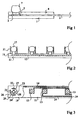
- FIG. 1 This patent describes an electrode of the type shown in FIG. 1 which comprises a support plate 1 made of a rigid insulating material such as silicon or glass. On this plate is disposed an electrode consisting of a conductive layer 2 connected to a wire 3. This conductive layer has for example a thickness less than 0.1 microns. The whole of the wafer 1 is covered with an insulating layer 4 provided with an opening 5 facing the conductive layer 2. A cell, for example an island of Langerhans, is disposed on the opening 5 so as to adhere the conductive layer 2 and the walls of the insulating layer 4.
- the exposed upper surface of the insulating layer on which the cells must at least partially grow (a part of each cell grows on the conductive plate and a part of the cell grows on the insulating layer) must be treated so that the cells grow on this layer and tend to adhere to it strongly and sealed "(column 4, lines 14 to 18) .It is also stated that” the strong adhesion and sealing between the cell and the insulating layer prevent the electrical signal from the cell from being attenuated by a short circuit between the cell or conductive plate and the environment surrounding the cell "(column 4, lines 22 to 26).
- the cell or island of Langerhans is very close to the corresponding electrode or in contact therewith. It is also expected that the part of the surrounding fluid trapped between the cell and the electrode is located in a closed enclosure by the walls of the opening 5, the conductive layer 2 and the cell 7.
- this document provides that several structures such as that illustrated in section in Figure 1 can be arranged in parallel on the same plate: the openings 5 are side by side and the son 3 are parallel to each other, in a perpendicular direction to the alignment direction of the cells.
- German patent application DE-A-197 12 309 relates to a microelectrode for small diameter cells (10 .mu.m ) in which contact between cells and electrodes is also sought.
- the features of the preamble of claim 1 are disclosed herein.
- Figure 1 the structure illustrated in Figure 1 is intended to be incorporated in a capsule. During this incorporation, it appears in practice that at least a portion of the islets of Langerhans are unhooked from the opening above which they must be located or aggregate with each other.
- An object according to the present invention is to overcome the disadvantages of this anterior electrode and to provide a higher electrode with a higher threshold of detectivity.
- the present invention provides a microelectrode for carrying at least one excitable membrane cell, comprising an insulating wafer provided with openings, each opening opening on a detection electrode and being surrounded by walls of insulating material substantially perpendicular to the wafer for locking said at least one cell in position, spacer means being provided for maintaining said at least one cell at a determined distance from the corresponding electrode.
- the spacer means are walls of insulating material substantially perpendicular to the wafer.
- the walls are formed from a multilayer structure of insulating material.
- the multilayer structure is formed by successive steps of spin coating and annealing of a polyimide.
- said opening is closed by an insulating wafer on which the electrode rests.
- said at least one excitable membrane cell is an island of Langerhans.
- microelectrodes are stacked, the walls of insulating material serving as spacers between two superposed electrodes.
- the thicknesses of the various layers and supports are not to scale and may be chosen conventionally by those skilled in the art.
- Fig. 2 is a sectional view schematically and partially showing a first embodiment of the present invention.
- an insulating support plate 11 for example a film of small thickness (a few microns), on which is deposited, for example by evaporation, a thin layer of a conductor, cram a metal, for example gold suitably etched to define conductive electrode plates and bonding tracks.
- a thin layer of a conductor for example by evaporation
- a metal for example gold suitably etched to define conductive electrode plates and bonding tracks.
- an example of conductive plates 13 and connecting tracks 14 can be seen.
- an insulating layer 19 is deposited. technique makes it possible to deposit layers having thicknesses of a few ⁇ m to a few tens of ⁇ m depending on the rotational speed of the spinner.
- the insulating layer 19 is provided with openings above the locations of the detecting electrodes, corresponding to Langerhans island positioning sites 17.
- each cell deposition site for example of Langerhans island
- lateral locking means for example four vertical walls 21-24.
- the spacing between these walls is chosen to be greater than or equal to the average value of the diameter of the cell or cells considered, this average value being generally of the order of 100 ⁇ m for a Langerhans island.
- the walls 21-24 may be made by deposition in thick layer, or preferably by successive deposits, an insulator and etching. For example, they will have a height slightly less than the diameter of an island of Langerhans.
- the etching may for example be carried out by reactive ion etching (RIE) in the presence of O 2 or CHF 3 or by excimer laser, which makes it possible to etch in a substantially vertical manner layers having thicknesses of the order of 100 ⁇ m. .
- RIE reactive ion etching
- the walls are "openwork" that is to say they do not form a continuous contour. In the example shown, they do not meet at the corners of the square they delimit. This is intended to allow nutrients (the medium in which the device will be placed) to reach all cells of the islet of Langerhans.
- spacing means are provided to cause the lower part of each island of Langerhans to be at a height substantially constant with respect to the corresponding detecting electrode.
- these spacing means consist of small walls 26-29, on whose vertices is based the island of Langerhans.
- the constituent materials of the elements of the electrode illustrated in Figures 2 and 3 will be chosen to allow simple manufacture and be biocompatible.
- the various insulating materials will be polyimides such as Dupont de Nemours polyimide PI 2611 and the conductive materials of the gold layers.
- the cells are represented as spaced apart by a distance greater than their diameter, it can be provided that the walls are arranged so that two neighboring cells are very close to one another, the walls to prevent two neighboring cells from clinging to each other.
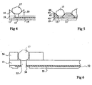
- Figures 4 to 6 show various alternative embodiments of a detector electrode site.
- the set of lateral blocking walls and spacing walls consists of a single structure.
- the walls 21-24 are replaced by walls 31-34 (only the walls 31 and 33 are visible in the sectional view).
- the wall 31 performs the functions of the lateral locking wall 21 and the spacer wall 26.
- the wall 33 performs the functions of the lateral locking wall 23 and the spacer wall 28.
- the walls 31 and 33 are relatively wide and have upper faces inclined inwardly.
- FIG. 5 represents a structure which is generally identical to that of FIG. 4 but which results from a deposition of multiple layers which are successively etched in a suitable manner to form the stepped inclined planes.
- a succession of layers 41, 42, 43, 44 is deposited, for example about ten successive layers each having a thickness of the order of a few ⁇ m to a few tens of ⁇ m, each layer in a first material being covered with a very thin layer of a second material serving as etching stop.
- Successive engravings are then carried out in concentric windows that are increasingly narrow to obtain the staircase structures represented.
- FIG. 6 shows another embodiment which differs from the previous embodiments essentially because the conductive layer constituting the detector electrode is not placed at the bottom of an opening corresponding to a blind hole, but on the opposite face compared to the island of Langerhans with a through opening.
- a relatively thick but flexible support 51 whose lower face is coated with a metallization 52.
- an insulating protection layer 53 is deposited on this metallization.
- the layer 53 is eliminated locally to reveal a detector electrode area 54 at each detection site.
- the support plate 51 is opened by a through hole 55 so that the detector electrode 54 constitutes a peripheral ring at the opening on the side of the lower face of the wafer 51.
- the thickness of the wafer 51 constitutes the fixing means of fixing the distance between the lower portion of the island of Langerhans 17 and the detector electrode 54.
- a thick layer of insulating material 56 having openings wider than the openings 55 at each site of detection. This layer 56 and the corresponding openings correspond to the lateral locking means described above.
- the opening 55 is a through opening, nutrients can arrive from the lower side of the Langerhans island through this opening.
- the wall 56 laterally blocking the island of Langerhans is openwork.
- a circular opening in a thick layer may be provided.
Landscapes
- Health & Medical Sciences (AREA)
- Life Sciences & Earth Sciences (AREA)
- Engineering & Computer Science (AREA)
- Biomedical Technology (AREA)
- Physics & Mathematics (AREA)
- General Health & Medical Sciences (AREA)
- Biophysics (AREA)
- Molecular Biology (AREA)
- Pathology (AREA)
- Chemical & Material Sciences (AREA)
- Immunology (AREA)
- Heart & Thoracic Surgery (AREA)
- Analytical Chemistry (AREA)
- Biochemistry (AREA)
- Food Science & Technology (AREA)
- General Physics & Mathematics (AREA)
- Hematology (AREA)
- Urology & Nephrology (AREA)
- Cardiology (AREA)
- Medicinal Chemistry (AREA)
- Medical Informatics (AREA)
- Surgery (AREA)
- Animal Behavior & Ethology (AREA)
- Public Health (AREA)
- Veterinary Medicine (AREA)
- Apparatus Associated With Microorganisms And Enzymes (AREA)
- Measuring Or Testing Involving Enzymes Or Micro-Organisms (AREA)
- Immobilizing And Processing Of Enzymes And Microorganisms (AREA)
- Micro-Organisms Or Cultivation Processes Thereof (AREA)
Abstract
Description
La présente invention concerne un détecteur de glycémie, et plus particulièrement une électrode de très petites dimensions susceptible de détecter l'activité électrique d'une cellule ou d'un amas de cellules à membrane excitable, par exemple des neurones, des cellules nodales autonomes du coeur ou des îlots de Langerhans.The present invention relates to a glucose detector, and more particularly to a very small electrode capable of detecting the electrical activity of a cell or a cluster of excitable membrane cells, for example neurons, autonomous nodal cells of the heart or islets of Langerhans.
De telles électrodes sont connues dans la technique et ont en particulier été décrites dans le brevet américain 5513636 de la société israélienne CB-Carmel Biotechnology Ltd.Such electrodes are known in the art and have in particular been described in US Pat. No. 5,513,636 of the Israeli company CB-Carmel Biotechnology Ltd.
Ce brevet décrit une électrode du type de celle représentée en figure 1 qui comprend une plaquette support 1 en un matériau isolant rigide tel que du silicium ou du verre. Sur cette plaquette est disposée une électrode constituée d'une couche conductrice 2 reliée à un fil 3. Cette couche conductrice a par exemple une épaisseur inférieure à 0,1 µm. L'ensemble de la plaquette 1 est recouvert d'une couche isolante 4 munie d'une ouverture 5 en regard de la couche conductrice 2. Une cellule, par exemple un îlot de Langerhans, est disposée sur l'ouverture 5 de façon à adhérer à la couche conductrice 2 et aux parois de la couche isolante 4. Il est précisé que "la surface supérieure exposée de la couche isolante sur laquelle les cellules doivent être amenées à croître au moins partiellement (une partie de chaque cellule croît sur la plaque conductrice et une partie de la cellule croît sur la couche isolante) doit être traitée pour que les cellules croissent sur cette couche et tendent à y adhérer de façon forte et étanche" (colonne 4, lignes 14 à 18). Il est également précisé que "la forte adhérence et le scellement entre la cellule et la couche isolante empêchent le signal électrique en provenance de la cellule d'être atténué par un court-circuit entre la cellule ou la plaque conductrice et le milieu environnant la cellule" (colonne 4, lignes 22 à 26).This patent describes an electrode of the type shown in FIG. 1 which comprises a
Ainsi, dans ce brevet, il est prévu que la cellule ou l'îlot de Langerhans est très proche de l'électrode correspondante ou en contact avec celle-ci. Il est également prévu que la partie du fluide environnant piégée entre la cellule et l'électrode est située dans une enceinte close par les parois de l'ouverture 5, la couche conductrice 2 et la cellule 7.Thus, in this patent, it is provided that the cell or island of Langerhans is very close to the corresponding electrode or in contact therewith. It is also expected that the part of the surrounding fluid trapped between the cell and the electrode is located in a closed enclosure by the walls of the opening 5, the conductive layer 2 and the
En outre, ce document prévoit que plusieurs structures telles que celle illustrée en coupe en figure 1 peuvent être disposées en parallèle sur une même plaquette : les ouvertures 5 sont côte à côte et les fils 3 sont parallèles les uns aux autres, dans une direction perpendiculaire à la direction d'alignement des cellules.In addition, this document provides that several structures such as that illustrated in section in Figure 1 can be arranged in parallel on the same plate: the openings 5 are side by side and the
La demande de brevet allemand DE-A-197 12 309 vise une microélectrode pour des cellules de petit diamètre (10 µm) dans laquelle on recherche également un contact entre cellules et électrodes. Les caractéristiques du préambule de la revendication 1 sont divulgées dans ce document.German patent application DE-A-197 12 309 relates to a microelectrode for small diameter cells (10 .mu.m ) in which contact between cells and electrodes is also sought. The features of the preamble of
La demanderesse a constaté qu'en pratique les signaux électriques détectés par de telles électrodes n'étaient pas optimaux et a cherché à augmenter la détectivité des électrodes.The Applicant has found that in practice the electrical signals detected by such electrodes were not optimal and sought to increase the detectivity of the electrodes.
Par ailleurs, la structure illustrée en figure 1 est destinée à être incorporée dans une capsule. Lors de cette incorporation, il apparaît en pratique qu'au moins une partie des îlots de Langerhans se décrochent de l'ouverture au-dessus de laquelle ils doivent être situés ou s'agrègent entre eux.Furthermore, the structure illustrated in Figure 1 is intended to be incorporated in a capsule. During this incorporation, it appears in practice that at least a portion of the islets of Langerhans are unhooked from the opening above which they must be located or aggregate with each other.
Un objet selon la présente invention est de pallier les inconvénients de cette électrode antérieure et de prévoir une électrode à seuil de détectivité plus élevé.An object according to the present invention is to overcome the disadvantages of this anterior electrode and to provide a higher electrode with a higher threshold of detectivity.
Pour atteindre ces objets, la présente invention prévoit une microélectrode destinée à porter au moins une cellule à membrane excitable, comprenant une plaquette isolante munie d'ouvertures, chaque ouverture débouchant sur une électrode de détection et étant entourée de murs en matériau isolant sensiblement perpendiculaires à la plaquette pour bloquer en position ladite au moins une cellule, des moyens d'écartement étant prévus pour maintenir ladite au moins une cellule à une distance déterminée de l'électrode correspondante.To achieve these objects, the present invention provides a microelectrode for carrying at least one excitable membrane cell, comprising an insulating wafer provided with openings, each opening opening on a detection electrode and being surrounded by walls of insulating material substantially perpendicular to the wafer for locking said at least one cell in position, spacer means being provided for maintaining said at least one cell at a determined distance from the corresponding electrode.
Selon un mode de réalisation de la présente invention, les moyens d'écartement sont des murs en matériau isolant, sensiblement perpendiculaires à la plaquette.According to one embodiment of the present invention, the spacer means are walls of insulating material substantially perpendicular to the wafer.
Selon un mode de réalisation de la présente invention, les murs sont formés à partir d'une structure multicouche de matériau isolant.According to one embodiment of the present invention, the walls are formed from a multilayer structure of insulating material.
Selon un mode de réalisation de la présente invention, la structure multicouche est formée par des étapes successives de dépôt à la tournette et de recuit d'un polyimide.According to one embodiment of the present invention, the multilayer structure is formed by successive steps of spin coating and annealing of a polyimide.
Selon un mode de réalisation de la présente invention, ladite ouverture est fermée par une plaquette isolante sur laquelle repose l'électrode.According to one embodiment of the present invention, said opening is closed by an insulating wafer on which the electrode rests.
Selon un mode de réalisation de la présente invention, ladite au moins une cellule à membrane excitable est un îlot de Langerhans.According to one embodiment of the present invention, said at least one excitable membrane cell is an island of Langerhans.
Selon un mode de réalisation de la présente invention, plusieurs microélectrodes sont empilées, les murs en matériau isolant servant d'entretoises entre deux électrodes superposées.According to one embodiment of the present invention, several microelectrodes are stacked, the walls of insulating material serving as spacers between two superposed electrodes.
Ces objets, caractéristiques et avantages, ainsi que d'autres de la présente invention seront exposés en détail dans la description suivante de modes de réalisation particuliers faite à titre non-limitatif en relation avec les figures jointes parmi lesquelles :
- la figure 1 est une vue en coupe partielle et schématique d'une électrode selon l'art antérieur ;
- la figure 2 est une vue en coupe schématique et partielle d'une électrode selon un mode de réalisation de la présente invention ;
- la figure 3 est une vue de dessus schématique de l'électrode de la figure 2 ;
- la figure 4 est une vue en coupe partielle illustrant un autre mode de réalisation ne faisant pas partie de la présente invention ;
- la figure 5 est une vue en coupe partielle illustrant un autre mode de réalisations ne faisant pas partie de la présente invention ; et
- la figure 6 est une vue en coupe partielle illustrant un autre mode de réalisation ne faisant pas partie de la présente invention.
- Figure 1 is a partial and schematic sectional view of an electrode according to the prior art;
- Figure 2 is a schematic and partial sectional view of an electrode according to an embodiment of the present invention;
- Figure 3 is a schematic top view of the electrode of Figure 2;
- Figure 4 is a partial sectional view illustrating another embodiment not forming part of the present invention;
- Figure 5 is a partial sectional view illustrating another embodiment not forming part of the present invention; and
- Figure 6 is a partial sectional view illustrating another embodiment not forming part of the present invention.
Dans les diverses figures, les épaisseurs des diverses couches et supports ne sont pas à l'échelle et pourront être choisies de façon classique par l'homme du métier.In the various figures, the thicknesses of the various layers and supports are not to scale and may be chosen conventionally by those skilled in the art.
La figure 2 est une vue en coupe représentant de façon schématique et partielle un premier mode de réalisation de la présente invention. On part d'une plaquette support isolante 11, par exemple un film de faible épaisseur (quelques µm), sur laquelle on dépose, par exemple par évaporation, une couche mince d'un conducteur, couramnent un métal, par exemple de l'or, convenablement gravée pour définir des plaques conductrices formant électrodes et des pistes de liaison. Dans la partie droite de la vue de dessus partiellement écorchée de la figure 3, on peut voir un exemple de plaques conductrices 13 et de pistes de liaison 14. On dépose ensuite, par exemple par dépôt à la tournette, une couche isolante 19. Cette technique permet de déposer des couches ayant des épaisseurs de quelques µm à quelques dizaines de µm selon la vitesse de rotation de la tournette. On pourra par exemple déposer une couche de polyimide mélangé à un solvant et ensuite recuit. La couche isolante 19 est munie d'ouvertures au-dessus des emplacements des électrodes détectrices, correspondant à des sites de positionnement d'îlots de Langerhans 17.Fig. 2 is a sectional view schematically and partially showing a first embodiment of the present invention. Starting from an
Selon un aspect de la présente invention, chaque site de dépôt de cellules, par exemple d'îlot de Langerhans, est encadré de moyens de blocage latéraux, par exemple quatre murs verticaux 21-24. L'espacement entre ces murs est choisi pour être supérieure ou égale à la valeur moyenne du diamètre de la ou des cellules considérées, cette valeur moyenne étant généralement de l'ordre de 100 µm pour un îlot de Langerhans. Les murs 21-24 pourront être réalisés par dépôt en couche épaisse, ou de préférence par dépôts successifs, d'un isolant et gravure. Ils auront par exemple une hauteur légèrement inférieure au diamètre d'un îlot de Langerhans. La gravure peut par exemple être réalisée par gravure ionique réactive (RIE) en présence d'O2 ou de CHF3 ou par laser excimère, ce qui permet de graver de façon sensiblement verticale des couches ayant des épaisseurs de l'ordre de 100 µm. Comme cela se voit en figure 3, les murs sont "ajourés" c'est-à-dire qu'ils ne forment pas un contour continu. Dans l'exemple représenté, ils ne se rejoignent pas au niveau des coins du carré qu'ils délimitent. Ceci est destiné à permettre à des nutriments (le milieu dans lequel le dispositif va être placé) d'atteindre toutes les cellules de l'îlot de Langerhans.According to one aspect of the present invention, each cell deposition site, for example of Langerhans island, is framed by lateral locking means, for example four vertical walls 21-24. The spacing between these walls is chosen to be greater than or equal to the average value of the diameter of the cell or cells considered, this average value being generally of the order of 100 μm for a Langerhans island. The walls 21-24 may be made by deposition in thick layer, or preferably by successive deposits, an insulator and etching. For example, they will have a height slightly less than the diameter of an island of Langerhans. The etching may for example be carried out by reactive ion etching (RIE) in the presence of O 2 or CHF 3 or by excimer laser, which makes it possible to etch in a substantially vertical manner layers having thicknesses of the order of 100 μm. . As can be seen in Figure 3, the walls are "openwork" that is to say they do not form a continuous contour. In the example shown, they do not meet at the corners of the square they delimit. This is intended to allow nutrients (the medium in which the device will be placed) to reach all cells of the islet of Langerhans.
Selon un deuxième aspect de la présente invention, il est prévu des moyens d'espacement pour amener la partie basse de chaque îlot de Langerhans à se trouver à une hauteur sensiblement constante par rapport à l'électrode détectrice correspondante. En effet, selon cet aspect de la présente invention, il a été déterminé que l'on augmente de façon importante la tension détectée par une électrode quand la distance entre la partie basse d'un îlot de Langerhans et l'électrode détectrice correspondante a une valeur déterminée, faible mais non nulle. On pourra choisir une distance de l'ordre de la moitié du diamètre de l'Îlot de Langerhans, par exemple comprise entre 0, 2 et 0, 7 fois le diamètre de l'îlot de Langerhans, bien que d'autres valeurs soient possibles. Pour d'autres cellules ou groupes de cellules on pourra de même choisir une distance optimale.According to a second aspect of the present invention, spacing means are provided to cause the lower part of each island of Langerhans to be at a height substantially constant with respect to the corresponding detecting electrode. Indeed, according to this aspect of the present invention, it has been determined that the voltage detected by an electrode is significantly increased when the distance between the lower part of a Langerhans island and the corresponding detector electrode has a difference. determined value, low but not zero. We can choose a distance of the order of half the diameter of the island of Langerhans, for example between 0, 2 and 0.7 times the diameter of the island of Langerhans, although other values are possible. For other cells or groups of cells it will be possible to choose an optimal distance.
Dans le cas des figures 2 et 3, ces moyens d'espacement sont constitués de petits murs 26-29, sur les sommets desquels s'appuie l'îlot de Langerhans.In the case of Figures 2 and 3, these spacing means consist of small walls 26-29, on whose vertices is based the island of Langerhans.
Les matériaux constitutifs des éléments de l'électrode illustrée en figures 2 et 3 seront choisis pour permettre une fabrication simple et être biocompatibles. Par exemple, les divers matériaux isolants seront des polyimides tels que le polyimide PI 2611 de Dupont de Nemours et les matériaux conducteurs des couches d'or.The constituent materials of the elements of the electrode illustrated in Figures 2 and 3 will be chosen to allow simple manufacture and be biocompatible. For example, the various insulating materials will be polyimides such as Dupont de Nemours polyimide PI 2611 and the conductive materials of the gold layers.
Comme le représente la figure 3, sur une même plaquette d'électrodes, on prévoira plusieurs sites disposés les uns derrière les autres dans le sens de la longueur de la plaquette. Ceci conduit à la réalisation d'un ensemble d'électrodes de petite dimension et particulièrement simple à implanter dans une capsule destinée à être placée dans le corps d'un patient. Bien que, pour clarifier la représentation, les cellules soient représentées comme espacées d'une distance supérieure à leur diamètre, on pourra prévoir que les murs sont disposés de telle sorte que deux cellules voisines sont très proches l'une de l'autre, les murs permettant d'éviter que deux cellules voisines ne s'aggrippent l'une à l'autre.As shown in Figure 3, on the same pad of electrodes, there will be provided several sites arranged one behind the other in the direction of the length of the wafer. This leads to the realization of a set of small electrodes and particularly simple to implant in a capsule to be placed in the body of a patient. Although, to clarify the representation, the cells are represented as spaced apart by a distance greater than their diameter, it can be provided that the walls are arranged so that two neighboring cells are very close to one another, the walls to prevent two neighboring cells from clinging to each other.
Selon un aspect de la présente invention, on pourra prévoir des murs de séparation plus hauts que le diamètre d'une cellule et empiler plusieurs microélectrodes, les murs de séparation servant d'entretoises entre deux microélectrodes superposées.According to one aspect of the present invention, it will be possible to provide separation walls higher than the diameter of a cell and to stack a plurality of microelectrodes, the partition walls serving as spacers between two superimposed microelectrodes.
Les figures 4 à 6 représentent diverses variantes de réalisation d'un site d'électrode détectrice.Figures 4 to 6 show various alternative embodiments of a detector electrode site.
Dans les modes de réalisation des figures 4 et 5, l'ensemble des murs de blocage latéraux et des murs d'espacement est constitué d'une seule et même structure.In the embodiments of FIGS. 4 and 5, the set of lateral blocking walls and spacing walls consists of a single structure.
Dans le cas de la figure 4, les murs 21-24 sont remplacés par des murs 31-34 (seuls les murs 31 et 33 sont visibles dans la vue en coupe) . Le mur 31 assure les fonctions du mur de blocage latéral 21 et du mur d'espacement 26. De même, le mur 33 assure les fonctions du mur de blocage latéral 23 et du mur d'espacement 28. A cette fin, les murs 31 et 33 sont relativement larges et ont des faces supérieures inclinées vers l'intérieur.In the case of Figure 4, the walls 21-24 are replaced by walls 31-34 (only the
La figure 5 représente une structure qui est globalement identique à celle de la figure 4 mais qui résulte d'un dépôt de couches multiples qui sont successivement gravées de façon appropriée pour former les plans inclinés en escalier. Ainsi, on dépose une succession de couches 41, 42, 43, 44 ..., par exemple une dizaine de couches successives ayant chacune une épaisseur de l'ordre de quelques µm à quelques dizaines de µm, chaque couche en un premier matériau étant recouverte d'une couche très mince d'un deuxième matériau servant d'arrêt de gravure. On procède ensuite à des gravures successives selon des fenêtres concentriques de plus en plus étroites pour obtenir les structures en escalier représentées. Inversement, on pourra après chaque dépôt procéder à une gravure, les couches successives étant gravées pour former des ouvertures plus larges que des ouvertures précédentes, et centrées sur celles-ci.FIG. 5 represents a structure which is generally identical to that of FIG. 4 but which results from a deposition of multiple layers which are successively etched in a suitable manner to form the stepped inclined planes. Thus, a succession of
La figure 6 représente un autre mode de réalisation qui diffère des modes de réalisation précédents essentiellement du fait que la couche conductrice constituant l'électrode détectrice n'est pas placée au fond d'une ouverture correspondant à un trou borgne, mais sur la face opposée par rapport à l'îlot de Langerhans d'une ouverture traversante. Dans le mode de réalisation de la figure 6, on part d'un support relativement épais mais souple 51 dont la face inférieure est revêtue d'une métallisation 52. Sur cette métallisation est déposée une couche isolante de protection 53. La couche 53 est éliminée localement pour laisser apparaître une zone d'électrode détectrice 54 au niveau de chaque site de détection. Au niveau de chacun de ces sites, la plaquette support 51 est ouverte par un trou traversant 55 de sorte que l'électrode détectrice 54 constitue un anneau périphérique à l'ouverture du côté de la face inférieure de la plaquette 51. Dans ce mode de réalisation, l'épaisseur de la plaquette 51 constitue le moyen d'écartement fixant la distance entre la partie inférieure de l'îlot de Langerhans 17 et l'électrode détectrice 54. Du côté de la face supérieure est déposée une couche épaisse de matériau isolant 56 comportant des ouvertures plus larges que les ouvertures 55 au niveau de chaque site de détection. Cette couche 56 et les ouvertures correspondantes correspondent au moyen de blocage latéral décrit précédemment.FIG. 6 shows another embodiment which differs from the previous embodiments essentially because the conductive layer constituting the detector electrode is not placed at the bottom of an opening corresponding to a blind hole, but on the opposite face compared to the island of Langerhans with a through opening. In the embodiment of FIG. 6, starting from a relatively thick but
Dans le mode de réalisation de la figure 6, on notera que, du fait que l'ouverture 55 est une ouverture traversante, des nutriments peuvent arriver du côté inférieur de l'îlot de Langerhans par cette ouverture. Ainsi, il n'est pas nécessaire que le mur 56 bloquant latéralement l'îlot de Langerhans soit ajouré. On pourra prévoir, par exemple, une ouverture circulaire dans une couche épaisse.In the embodiment of FIG. 6, it will be noted that, since the
Claims (7)
- A microelectrode intended to support at least one cell with an excitable membrane immerged in a fluid, including an insulating support plate (11) and an insulating layer (19) provided with openings, each opening emerging on a detection electrode (13) and being surrounded with walls (21-24) made of insulating material, substantially perpendicular to the plate to block in position said at least one cell, characterized in that it further includes spacing means (26-29) for maintaining said at least one cell at a determined distance from the corresponding electrode, said distance being occupied by said fluid.
- The microelectrode of claim 1, characterized in that the spacing means are walls made of an insulating material, substantially perpendicular to the plate.
- The microelectrode of claim 1, characterized in that the walls are formed from a multiple-layer structure of insulating material.
- The microelectrode of claim 3, characterized in that the multiple-layer structure is formed by successive steps of spin-on deposition and of anneal of a polyimide.
- The microelectrode of claim 1, wherein said opening is closed by an insulating plate on which the electrode is laid.
- The microelectrode of claim 1, characterized in that said at least one cell with an excitable membrane is an islet of Langerhans.
- A stack of the microelectrodes of any of claims 1 to 6, in which the walls of insulating material to block in position said at least one cell are used as spacers between two superposed microelectrodes.
Applications Claiming Priority (3)
| Application Number | Priority Date | Filing Date | Title |
|---|---|---|---|
| FR9915772A FR2802078B1 (en) | 1999-12-14 | 1999-12-14 | MICROELECTRODE CELL SUPPORT WITH EXCITABLE MEMBRANE |
| FR9915772 | 1999-12-14 | ||
| PCT/FR2000/003543 WO2001043636A1 (en) | 1999-12-14 | 2000-12-14 | Microelectrode supporting cell with excitable membrane |
Publications (2)
| Publication Number | Publication Date |
|---|---|
| EP1237474A1 EP1237474A1 (en) | 2002-09-11 |
| EP1237474B1 true EP1237474B1 (en) | 2006-03-08 |
Family
ID=9553254
Family Applications (1)
| Application Number | Title | Priority Date | Filing Date |
|---|---|---|---|
| EP00988922A Expired - Lifetime EP1237474B1 (en) | 1999-12-14 | 2000-12-14 | Microelectrode supporting cell with excitable membrane |
Country Status (7)
| Country | Link |
|---|---|
| US (1) | US20030078483A1 (en) |
| EP (1) | EP1237474B1 (en) |
| JP (1) | JP2003517148A (en) |
| AT (1) | ATE319372T1 (en) |
| DE (1) | DE60026609T2 (en) |
| FR (1) | FR2802078B1 (en) |
| WO (1) | WO2001043636A1 (en) |
Families Citing this family (1)
| Publication number | Priority date | Publication date | Assignee | Title |
|---|---|---|---|---|
| JP6218199B1 (en) * | 2016-10-06 | 2017-10-25 | 日本航空電子工業株式会社 | Electrochemical measuring device and transducer |
Citations (2)
| Publication number | Priority date | Publication date | Assignee | Title |
|---|---|---|---|---|
| WO2001025769A2 (en) * | 1999-10-01 | 2001-04-12 | Sophion Bioscience A/S | A substrate and a method for determining and/or monitoring electrophysiological properties of ion channels |
| EP1218736A1 (en) * | 1999-10-08 | 2002-07-03 | Nmi Naturwissenschaftliches Und Medizinisches Institut An Der Universität Tübingen | Method and device for taking measurements of cells which are contained in a liquid environment |
Family Cites Families (4)
| Publication number | Priority date | Publication date | Assignee | Title |
|---|---|---|---|---|
| US5513636A (en) * | 1994-08-12 | 1996-05-07 | Cb-Carmel Biotechnology Ltd. | Implantable sensor chip |
| DE19712309A1 (en) * | 1996-11-16 | 1998-05-20 | Nmi Univ Tuebingen | Microelement arrangement, method for contacting cells in a liquid environment and method for producing a microelement arrangement |
| EP0938674B1 (en) * | 1996-11-16 | 2005-06-01 | NMI Naturwissenschaftliches und Medizinisches Institut an der Universität Tübingen in Reutlingen Stiftung Bürgerlichen Rechts | Array of microelements, method of contacting cells in a liquid environment and method for the production of an array of microelements |
| US20020144905A1 (en) * | 1997-12-17 | 2002-10-10 | Christian Schmidt | Sample positioning and analysis system |
-
1999
- 1999-12-14 FR FR9915772A patent/FR2802078B1/en not_active Expired - Fee Related
-
2000
- 2000-12-14 DE DE60026609T patent/DE60026609T2/en not_active Expired - Lifetime
- 2000-12-14 WO PCT/FR2000/003543 patent/WO2001043636A1/en not_active Ceased
- 2000-12-14 EP EP00988922A patent/EP1237474B1/en not_active Expired - Lifetime
- 2000-12-14 AT AT00988922T patent/ATE319372T1/en not_active IP Right Cessation
- 2000-12-14 US US10/168,123 patent/US20030078483A1/en not_active Abandoned
- 2000-12-14 JP JP2001544579A patent/JP2003517148A/en not_active Withdrawn
Patent Citations (2)
| Publication number | Priority date | Publication date | Assignee | Title |
|---|---|---|---|---|
| WO2001025769A2 (en) * | 1999-10-01 | 2001-04-12 | Sophion Bioscience A/S | A substrate and a method for determining and/or monitoring electrophysiological properties of ion channels |
| EP1218736A1 (en) * | 1999-10-08 | 2002-07-03 | Nmi Naturwissenschaftliches Und Medizinisches Institut An Der Universität Tübingen | Method and device for taking measurements of cells which are contained in a liquid environment |
Also Published As
| Publication number | Publication date |
|---|---|
| DE60026609D1 (en) | 2006-05-04 |
| FR2802078A1 (en) | 2001-06-15 |
| JP2003517148A (en) | 2003-05-20 |
| WO2001043636A1 (en) | 2001-06-21 |
| US20030078483A1 (en) | 2003-04-24 |
| ATE319372T1 (en) | 2006-03-15 |
| DE60026609T2 (en) | 2006-12-28 |
| FR2802078B1 (en) | 2003-10-03 |
| EP1237474A1 (en) | 2002-09-11 |
Similar Documents
| Publication | Publication Date | Title |
|---|---|---|
| EP0557217B1 (en) | Capacitive micro-sensor with reduced parasitic capacitance and method of manufacturing the same | |
| EP0596456B1 (en) | Method of manufacturing an integrated capacitive transductor | |
| EP4062451B1 (en) | Method for manufacturing a detection device having improved getter protection | |
| EP0983609B1 (en) | Method for making a machined silicon micro-sensor | |
| EP3476284B1 (en) | Biocompatible integrated monolithic sensor, notably for an active implantable medical device | |
| FR2829876A1 (en) | PHOTOSENSITIVE CELL INCORPORATING A LIGHT GUIDE AND MATRIX COMPOSED OF SUCH CELLS | |
| EP0866972B1 (en) | Accelerometer and method for making same | |
| EP1237474B1 (en) | Microelectrode supporting cell with excitable membrane | |
| EP3633336B1 (en) | Pyroelectric detection device with rigid membrane | |
| EP1260813A1 (en) | System of electrodes for an electrochemical sensor | |
| FR2738705A1 (en) | ELECTROMECHANICAL SENSOR DEVICE AND METHOD FOR MANUFACTURING SUCH A DEVICE | |
| EP0279752B1 (en) | Method of producing metallised through-holes with different heights | |
| FR2746678A1 (en) | METHOD FOR MAKING A DEPOSIT ON A REMOVABLE MEDIUM, AND DEPOSIT CARRIED OUT ON A MEDIUM | |
| WO2021239737A1 (en) | Photovoltaic cell and string and associated methods | |
| EP4528806B1 (en) | Electronic chip comprising connection pillars | |
| EP4593074A1 (en) | Electronic component comprising connection pillars | |
| EP1557665A1 (en) | Electrode system for an electrochemical sensor | |
| EP4069884A1 (en) | Forming nanowires | |
| FR3099953A1 (en) | Collective manufacturing process of a pyroelectric detector | |
| FR2938974A1 (en) | MICROELECTROMECHANICAL COMPONENT AND METHOD OF MANUFACTURE | |
| FR3087006A1 (en) | PYROELECTRIC SENSOR WITH SUSPENDED MEMBRANE | |
| WO2002091556A1 (en) | Electrostatic actuator | |
| WO2005029063A1 (en) | Method for producing electrodes, an integrated circuit provided with protected electrode (s) and an electrochemical sensor |
Legal Events
| Date | Code | Title | Description |
|---|---|---|---|
| PUAI | Public reference made under article 153(3) epc to a published international application that has entered the european phase |
Free format text: ORIGINAL CODE: 0009012 |
|
| 17P | Request for examination filed |
Effective date: 20020705 |
|
| AK | Designated contracting states |
Kind code of ref document: A1 Designated state(s): AT BE CH CY DE DK ES FI FR GB GR IE IT LI LU MC NL PT SE TR |
|
| 17Q | First examination report despatched |
Effective date: 20050302 |
|
| GRAP | Despatch of communication of intention to grant a patent |
Free format text: ORIGINAL CODE: EPIDOSNIGR1 |
|
| GRAS | Grant fee paid |
Free format text: ORIGINAL CODE: EPIDOSNIGR3 |
|
| GRAA | (expected) grant |
Free format text: ORIGINAL CODE: 0009210 |
|
| RAP1 | Party data changed (applicant data changed or rights of an application transferred) |
Owner name: MICROVITAE TECHNOLOGIES |
|
| AK | Designated contracting states |
Kind code of ref document: B1 Designated state(s): AT BE CH CY DE DK ES FI FR GB GR IE IT LI LU MC NL PT SE TR |
|
| PG25 | Lapsed in a contracting state [announced via postgrant information from national office to epo] |
Ref country code: FI Free format text: LAPSE BECAUSE OF FAILURE TO SUBMIT A TRANSLATION OF THE DESCRIPTION OR TO PAY THE FEE WITHIN THE PRESCRIBED TIME-LIMIT Effective date: 20060308 Ref country code: NL Free format text: LAPSE BECAUSE OF FAILURE TO SUBMIT A TRANSLATION OF THE DESCRIPTION OR TO PAY THE FEE WITHIN THE PRESCRIBED TIME-LIMIT Effective date: 20060308 Ref country code: IE Free format text: LAPSE BECAUSE OF FAILURE TO SUBMIT A TRANSLATION OF THE DESCRIPTION OR TO PAY THE FEE WITHIN THE PRESCRIBED TIME-LIMIT Effective date: 20060308 |
|
| REG | Reference to a national code |
Ref country code: GB Ref legal event code: FG4D Free format text: NOT ENGLISH |
|
| REG | Reference to a national code |
Ref country code: CH Ref legal event code: EP |
|
| REG | Reference to a national code |
Ref country code: IE Ref legal event code: FG4D Free format text: LANGUAGE OF EP DOCUMENT: FRENCH |
|
| REF | Corresponds to: |
Ref document number: 60026609 Country of ref document: DE Date of ref document: 20060504 Kind code of ref document: P |
|
| PG25 | Lapsed in a contracting state [announced via postgrant information from national office to epo] |
Ref country code: DK Free format text: LAPSE BECAUSE OF FAILURE TO SUBMIT A TRANSLATION OF THE DESCRIPTION OR TO PAY THE FEE WITHIN THE PRESCRIBED TIME-LIMIT Effective date: 20060608 Ref country code: SE Free format text: LAPSE BECAUSE OF FAILURE TO SUBMIT A TRANSLATION OF THE DESCRIPTION OR TO PAY THE FEE WITHIN THE PRESCRIBED TIME-LIMIT Effective date: 20060608 |
|
| PG25 | Lapsed in a contracting state [announced via postgrant information from national office to epo] |
Ref country code: ES Free format text: LAPSE BECAUSE OF FAILURE TO SUBMIT A TRANSLATION OF THE DESCRIPTION OR TO PAY THE FEE WITHIN THE PRESCRIBED TIME-LIMIT Effective date: 20060619 |
|
| GBT | Gb: translation of ep patent filed (gb section 77(6)(a)/1977) |
Effective date: 20060619 |
|
| PG25 | Lapsed in a contracting state [announced via postgrant information from national office to epo] |
Ref country code: PT Free format text: LAPSE BECAUSE OF FAILURE TO SUBMIT A TRANSLATION OF THE DESCRIPTION OR TO PAY THE FEE WITHIN THE PRESCRIBED TIME-LIMIT Effective date: 20060808 |
|
| NLV1 | Nl: lapsed or annulled due to failure to fulfill the requirements of art. 29p and 29m of the patents act | ||
| REG | Reference to a national code |
Ref country code: IE Ref legal event code: FD4D |
|
| PGFP | Annual fee paid to national office [announced via postgrant information from national office to epo] |
Ref country code: GB Payment date: 20061214 Year of fee payment: 7 |
|
| PGFP | Annual fee paid to national office [announced via postgrant information from national office to epo] |
Ref country code: AT Payment date: 20061219 Year of fee payment: 7 |
|
| PG25 | Lapsed in a contracting state [announced via postgrant information from national office to epo] |
Ref country code: MC Free format text: LAPSE BECAUSE OF NON-PAYMENT OF DUE FEES Effective date: 20061231 Ref country code: CH Free format text: LAPSE BECAUSE OF NON-PAYMENT OF DUE FEES Effective date: 20061231 Ref country code: BE Free format text: LAPSE BECAUSE OF NON-PAYMENT OF DUE FEES Effective date: 20061231 Ref country code: LI Free format text: LAPSE BECAUSE OF NON-PAYMENT OF DUE FEES Effective date: 20061231 |
|
| PLBE | No opposition filed within time limit |
Free format text: ORIGINAL CODE: 0009261 |
|
| STAA | Information on the status of an ep patent application or granted ep patent |
Free format text: STATUS: NO OPPOSITION FILED WITHIN TIME LIMIT |
|
| 26N | No opposition filed |
Effective date: 20061211 |
|
| REG | Reference to a national code |
Ref country code: CH Ref legal event code: PL |
|
| BERE | Be: lapsed |
Owner name: MICROVITAE TECHNOLOGIES Effective date: 20061231 |
|
| PGFP | Annual fee paid to national office [announced via postgrant information from national office to epo] |
Ref country code: IT Payment date: 20071129 Year of fee payment: 8 |
|
| PG25 | Lapsed in a contracting state [announced via postgrant information from national office to epo] |
Ref country code: GR Free format text: LAPSE BECAUSE OF FAILURE TO SUBMIT A TRANSLATION OF THE DESCRIPTION OR TO PAY THE FEE WITHIN THE PRESCRIBED TIME-LIMIT Effective date: 20060609 |
|
| PG25 | Lapsed in a contracting state [announced via postgrant information from national office to epo] |
Ref country code: LU Free format text: LAPSE BECAUSE OF NON-PAYMENT OF DUE FEES Effective date: 20061214 Ref country code: TR Free format text: LAPSE BECAUSE OF FAILURE TO SUBMIT A TRANSLATION OF THE DESCRIPTION OR TO PAY THE FEE WITHIN THE PRESCRIBED TIME-LIMIT Effective date: 20060308 |
|
| GBPC | Gb: european patent ceased through non-payment of renewal fee |
Effective date: 20071214 |
|
| PG25 | Lapsed in a contracting state [announced via postgrant information from national office to epo] |
Ref country code: AT Free format text: LAPSE BECAUSE OF NON-PAYMENT OF DUE FEES Effective date: 20071214 |
|
| PG25 | Lapsed in a contracting state [announced via postgrant information from national office to epo] |
Ref country code: CY Free format text: LAPSE BECAUSE OF FAILURE TO SUBMIT A TRANSLATION OF THE DESCRIPTION OR TO PAY THE FEE WITHIN THE PRESCRIBED TIME-LIMIT Effective date: 20060308 |
|
| PG25 | Lapsed in a contracting state [announced via postgrant information from national office to epo] |
Ref country code: GB Free format text: LAPSE BECAUSE OF NON-PAYMENT OF DUE FEES Effective date: 20071214 |
|
| PG25 | Lapsed in a contracting state [announced via postgrant information from national office to epo] |
Ref country code: IT Free format text: LAPSE BECAUSE OF NON-PAYMENT OF DUE FEES Effective date: 20081214 |
|
| PGFP | Annual fee paid to national office [announced via postgrant information from national office to epo] |
Ref country code: DE Payment date: 20150109 Year of fee payment: 15 |
|
| REG | Reference to a national code |
Ref country code: FR Ref legal event code: PLFP Year of fee payment: 16 |
|
| REG | Reference to a national code |
Ref country code: DE Ref legal event code: R119 Ref document number: 60026609 Country of ref document: DE |
|
| PG25 | Lapsed in a contracting state [announced via postgrant information from national office to epo] |
Ref country code: DE Free format text: LAPSE BECAUSE OF NON-PAYMENT OF DUE FEES Effective date: 20160701 |
|
| REG | Reference to a national code |
Ref country code: FR Ref legal event code: PLFP Year of fee payment: 17 |
|
| REG | Reference to a national code |
Ref country code: FR Ref legal event code: PLFP Year of fee payment: 18 |
|
| PGFP | Annual fee paid to national office [announced via postgrant information from national office to epo] |
Ref country code: FR Payment date: 20181218 Year of fee payment: 19 |
|
| PG25 | Lapsed in a contracting state [announced via postgrant information from national office to epo] |
Ref country code: FR Free format text: LAPSE BECAUSE OF NON-PAYMENT OF DUE FEES Effective date: 20191231 |