EP1237474B1 - Mikroelektrode zum tragen von zellen mit reizbarer membran - Google Patents
Mikroelektrode zum tragen von zellen mit reizbarer membran Download PDFInfo
- Publication number
- EP1237474B1 EP1237474B1 EP00988922A EP00988922A EP1237474B1 EP 1237474 B1 EP1237474 B1 EP 1237474B1 EP 00988922 A EP00988922 A EP 00988922A EP 00988922 A EP00988922 A EP 00988922A EP 1237474 B1 EP1237474 B1 EP 1237474B1
- Authority
- EP
- European Patent Office
- Prior art keywords
- cell
- microelectrode
- walls
- electrode
- insulating
- Prior art date
- Legal status (The legal status is an assumption and is not a legal conclusion. Google has not performed a legal analysis and makes no representation as to the accuracy of the status listed.)
- Expired - Lifetime
Links
- 239000012528 membrane Substances 0.000 title claims abstract description 7
- 239000011810 insulating material Substances 0.000 claims abstract description 12
- 125000006850 spacer group Chemical group 0.000 claims description 7
- 239000004642 Polyimide Substances 0.000 claims description 5
- 230000008021 deposition Effects 0.000 claims description 5
- 229920001721 polyimide Polymers 0.000 claims description 5
- 238000001514 detection method Methods 0.000 claims description 4
- 239000012530 fluid Substances 0.000 claims description 3
- 239000002365 multiple layer Substances 0.000 claims 2
- 239000010410 layer Substances 0.000 claims 1
- 210000004027 cell Anatomy 0.000 description 32
- 210000004153 islets of langerhan Anatomy 0.000 description 7
- 238000000151 deposition Methods 0.000 description 5
- 238000005530 etching Methods 0.000 description 4
- 239000000463 material Substances 0.000 description 3
- 238000000137 annealing Methods 0.000 description 2
- 230000000903 blocking effect Effects 0.000 description 2
- 239000002775 capsule Substances 0.000 description 2
- 239000004020 conductor Substances 0.000 description 2
- PCHJSUWPFVWCPO-UHFFFAOYSA-N gold Chemical compound [Au] PCHJSUWPFVWCPO-UHFFFAOYSA-N 0.000 description 2
- 239000010931 gold Substances 0.000 description 2
- 229910052737 gold Inorganic materials 0.000 description 2
- 238000001465 metallisation Methods 0.000 description 2
- 235000015097 nutrients Nutrition 0.000 description 2
- 238000001020 plasma etching Methods 0.000 description 2
- 238000004528 spin coating Methods 0.000 description 2
- WQZGKKKJIJFFOK-GASJEMHNSA-N Glucose Natural products OC[C@H]1OC(O)[C@H](O)[C@@H](O)[C@@H]1O WQZGKKKJIJFFOK-GASJEMHNSA-N 0.000 description 1
- 230000002238 attenuated effect Effects 0.000 description 1
- 239000000470 constituent Substances 0.000 description 1
- 230000000694 effects Effects 0.000 description 1
- 238000001704 evaporation Methods 0.000 description 1
- 230000008020 evaporation Effects 0.000 description 1
- 239000011521 glass Substances 0.000 description 1
- 239000008103 glucose Substances 0.000 description 1
- 239000007943 implant Substances 0.000 description 1
- 238000010348 incorporation Methods 0.000 description 1
- 239000012212 insulator Substances 0.000 description 1
- 238000004519 manufacturing process Methods 0.000 description 1
- 239000002184 metal Substances 0.000 description 1
- 229910052751 metal Inorganic materials 0.000 description 1
- 238000000034 method Methods 0.000 description 1
- 210000002569 neuron Anatomy 0.000 description 1
- 238000005192 partition Methods 0.000 description 1
- 230000002093 peripheral effect Effects 0.000 description 1
- 238000007789 sealing Methods 0.000 description 1
- 238000000926 separation method Methods 0.000 description 1
- 229910052710 silicon Inorganic materials 0.000 description 1
- 239000010703 silicon Substances 0.000 description 1
- 239000002904 solvent Substances 0.000 description 1
Images
Classifications
-
- G—PHYSICS
- G01—MEASURING; TESTING
- G01N—INVESTIGATING OR ANALYSING MATERIALS BY DETERMINING THEIR CHEMICAL OR PHYSICAL PROPERTIES
- G01N33/00—Investigating or analysing materials by specific methods not covered by groups G01N1/00 - G01N31/00
- G01N33/48—Biological material, e.g. blood, urine; Haemocytometers
- G01N33/483—Physical analysis of biological material
- G01N33/487—Physical analysis of biological material of liquid biological material
- G01N33/48707—Physical analysis of biological material of liquid biological material by electrical means
- G01N33/48728—Investigating individual cells, e.g. by patch clamp, voltage clamp
-
- A—HUMAN NECESSITIES
- A61—MEDICAL OR VETERINARY SCIENCE; HYGIENE
- A61B—DIAGNOSIS; SURGERY; IDENTIFICATION
- A61B5/00—Measuring for diagnostic purposes; Identification of persons
- A61B5/24—Detecting, measuring or recording bioelectric or biomagnetic signals of the body or parts thereof
- A61B5/25—Bioelectric electrodes therefor
- A61B5/279—Bioelectric electrodes therefor specially adapted for particular uses
- A61B5/28—Bioelectric electrodes therefor specially adapted for particular uses for electrocardiography [ECG]
- A61B5/282—Holders for multiple electrodes
Definitions
- the present invention relates to a glucose detector, and more particularly to a very small electrode capable of detecting the electrical activity of a cell or a cluster of excitable membrane cells, for example neurons, autonomous nodal cells of the heart or islets of Langerhans.
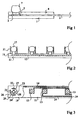
- FIG. 1 This patent describes an electrode of the type shown in FIG. 1 which comprises a support plate 1 made of a rigid insulating material such as silicon or glass. On this plate is disposed an electrode consisting of a conductive layer 2 connected to a wire 3. This conductive layer has for example a thickness less than 0.1 microns. The whole of the wafer 1 is covered with an insulating layer 4 provided with an opening 5 facing the conductive layer 2. A cell, for example an island of Langerhans, is disposed on the opening 5 so as to adhere the conductive layer 2 and the walls of the insulating layer 4.
- the exposed upper surface of the insulating layer on which the cells must at least partially grow (a part of each cell grows on the conductive plate and a part of the cell grows on the insulating layer) must be treated so that the cells grow on this layer and tend to adhere to it strongly and sealed "(column 4, lines 14 to 18) .It is also stated that” the strong adhesion and sealing between the cell and the insulating layer prevent the electrical signal from the cell from being attenuated by a short circuit between the cell or conductive plate and the environment surrounding the cell "(column 4, lines 22 to 26).
- the cell or island of Langerhans is very close to the corresponding electrode or in contact therewith. It is also expected that the part of the surrounding fluid trapped between the cell and the electrode is located in a closed enclosure by the walls of the opening 5, the conductive layer 2 and the cell 7.
- this document provides that several structures such as that illustrated in section in Figure 1 can be arranged in parallel on the same plate: the openings 5 are side by side and the son 3 are parallel to each other, in a perpendicular direction to the alignment direction of the cells.
- German patent application DE-A-197 12 309 relates to a microelectrode for small diameter cells (10 .mu.m ) in which contact between cells and electrodes is also sought.
- the features of the preamble of claim 1 are disclosed herein.
- Figure 1 the structure illustrated in Figure 1 is intended to be incorporated in a capsule. During this incorporation, it appears in practice that at least a portion of the islets of Langerhans are unhooked from the opening above which they must be located or aggregate with each other.
- An object according to the present invention is to overcome the disadvantages of this anterior electrode and to provide a higher electrode with a higher threshold of detectivity.
- the present invention provides a microelectrode for carrying at least one excitable membrane cell, comprising an insulating wafer provided with openings, each opening opening on a detection electrode and being surrounded by walls of insulating material substantially perpendicular to the wafer for locking said at least one cell in position, spacer means being provided for maintaining said at least one cell at a determined distance from the corresponding electrode.
- the spacer means are walls of insulating material substantially perpendicular to the wafer.
- the walls are formed from a multilayer structure of insulating material.
- the multilayer structure is formed by successive steps of spin coating and annealing of a polyimide.
- said opening is closed by an insulating wafer on which the electrode rests.
- said at least one excitable membrane cell is an island of Langerhans.
- microelectrodes are stacked, the walls of insulating material serving as spacers between two superposed electrodes.
- the thicknesses of the various layers and supports are not to scale and may be chosen conventionally by those skilled in the art.
- Fig. 2 is a sectional view schematically and partially showing a first embodiment of the present invention.
- an insulating support plate 11 for example a film of small thickness (a few microns), on which is deposited, for example by evaporation, a thin layer of a conductor, cram a metal, for example gold suitably etched to define conductive electrode plates and bonding tracks.
- a thin layer of a conductor for example by evaporation
- a metal for example gold suitably etched to define conductive electrode plates and bonding tracks.
- an example of conductive plates 13 and connecting tracks 14 can be seen.
- an insulating layer 19 is deposited. technique makes it possible to deposit layers having thicknesses of a few ⁇ m to a few tens of ⁇ m depending on the rotational speed of the spinner.
- the insulating layer 19 is provided with openings above the locations of the detecting electrodes, corresponding to Langerhans island positioning sites 17.
- each cell deposition site for example of Langerhans island
- lateral locking means for example four vertical walls 21-24.
- the spacing between these walls is chosen to be greater than or equal to the average value of the diameter of the cell or cells considered, this average value being generally of the order of 100 ⁇ m for a Langerhans island.
- the walls 21-24 may be made by deposition in thick layer, or preferably by successive deposits, an insulator and etching. For example, they will have a height slightly less than the diameter of an island of Langerhans.
- the etching may for example be carried out by reactive ion etching (RIE) in the presence of O 2 or CHF 3 or by excimer laser, which makes it possible to etch in a substantially vertical manner layers having thicknesses of the order of 100 ⁇ m. .
- RIE reactive ion etching
- the walls are "openwork" that is to say they do not form a continuous contour. In the example shown, they do not meet at the corners of the square they delimit. This is intended to allow nutrients (the medium in which the device will be placed) to reach all cells of the islet of Langerhans.
- spacing means are provided to cause the lower part of each island of Langerhans to be at a height substantially constant with respect to the corresponding detecting electrode.
- these spacing means consist of small walls 26-29, on whose vertices is based the island of Langerhans.
- the constituent materials of the elements of the electrode illustrated in Figures 2 and 3 will be chosen to allow simple manufacture and be biocompatible.
- the various insulating materials will be polyimides such as Dupont de Nemours polyimide PI 2611 and the conductive materials of the gold layers.
- the cells are represented as spaced apart by a distance greater than their diameter, it can be provided that the walls are arranged so that two neighboring cells are very close to one another, the walls to prevent two neighboring cells from clinging to each other.
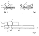
- Figures 4 to 6 show various alternative embodiments of a detector electrode site.
- the set of lateral blocking walls and spacing walls consists of a single structure.
- the walls 21-24 are replaced by walls 31-34 (only the walls 31 and 33 are visible in the sectional view).
- the wall 31 performs the functions of the lateral locking wall 21 and the spacer wall 26.
- the wall 33 performs the functions of the lateral locking wall 23 and the spacer wall 28.
- the walls 31 and 33 are relatively wide and have upper faces inclined inwardly.
- FIG. 5 represents a structure which is generally identical to that of FIG. 4 but which results from a deposition of multiple layers which are successively etched in a suitable manner to form the stepped inclined planes.
- a succession of layers 41, 42, 43, 44 is deposited, for example about ten successive layers each having a thickness of the order of a few ⁇ m to a few tens of ⁇ m, each layer in a first material being covered with a very thin layer of a second material serving as etching stop.
- Successive engravings are then carried out in concentric windows that are increasingly narrow to obtain the staircase structures represented.
- FIG. 6 shows another embodiment which differs from the previous embodiments essentially because the conductive layer constituting the detector electrode is not placed at the bottom of an opening corresponding to a blind hole, but on the opposite face compared to the island of Langerhans with a through opening.
- a relatively thick but flexible support 51 whose lower face is coated with a metallization 52.
- an insulating protection layer 53 is deposited on this metallization.
- the layer 53 is eliminated locally to reveal a detector electrode area 54 at each detection site.
- the support plate 51 is opened by a through hole 55 so that the detector electrode 54 constitutes a peripheral ring at the opening on the side of the lower face of the wafer 51.
- the thickness of the wafer 51 constitutes the fixing means of fixing the distance between the lower portion of the island of Langerhans 17 and the detector electrode 54.
- a thick layer of insulating material 56 having openings wider than the openings 55 at each site of detection. This layer 56 and the corresponding openings correspond to the lateral locking means described above.
- the opening 55 is a through opening, nutrients can arrive from the lower side of the Langerhans island through this opening.
- the wall 56 laterally blocking the island of Langerhans is openwork.
- a circular opening in a thick layer may be provided.
Landscapes
- Health & Medical Sciences (AREA)
- Life Sciences & Earth Sciences (AREA)
- Engineering & Computer Science (AREA)
- Biomedical Technology (AREA)
- Physics & Mathematics (AREA)
- General Health & Medical Sciences (AREA)
- Biophysics (AREA)
- Molecular Biology (AREA)
- Pathology (AREA)
- Chemical & Material Sciences (AREA)
- Immunology (AREA)
- Heart & Thoracic Surgery (AREA)
- Analytical Chemistry (AREA)
- Biochemistry (AREA)
- Food Science & Technology (AREA)
- General Physics & Mathematics (AREA)
- Hematology (AREA)
- Urology & Nephrology (AREA)
- Cardiology (AREA)
- Medicinal Chemistry (AREA)
- Medical Informatics (AREA)
- Surgery (AREA)
- Animal Behavior & Ethology (AREA)
- Public Health (AREA)
- Veterinary Medicine (AREA)
- Apparatus Associated With Microorganisms And Enzymes (AREA)
- Measuring Or Testing Involving Enzymes Or Micro-Organisms (AREA)
- Micro-Organisms Or Cultivation Processes Thereof (AREA)
- Immobilizing And Processing Of Enzymes And Microorganisms (AREA)
Claims (7)
- Mikroelektrode zur Aufnahme wenigstens einer in ein Strömungsmittel eingetauchten Zelle mit einer anregbaren Membran, welche eine isolierende Tragplatte bzw. -plakette (11) und eine mit Öffnungen versehene isolierende Schicht (19) aufweist, wobei jede Öffnung über einer Detektionselektrode (13) mündet und von Mauern bzw. Wandungen (21 - 24) aus einem isolierenden Material umgeben ist, die im wesentlichen senkrecht zu der Plakette sind, um die wenigstens eine Zelle in ihrer Stellung zu blockieren bzw. zu fixieren, dadurch gekennzeichnet, daß die Mikroelektrode des weiteren Abstandsmittel (26 - 29) aufweist, um die genannte wenigstens eine Zelle in einem vorgegebenen Abstand von der entsprechenden Elektrode zu halten, wobei dieser Abstand von dem genannten Strömungsmittel eingenommen wird.
- Mikroelektrode nach Anspruch 1, dadurch gekennzeichnet, daß die Abstandsmittel Mauern bzw. Wandungen aus einem isolierenden Material im wesentlichen senkrecht zu der Plakette sind.
- Mikroelektrode nach Anspruch 1, dadurch gekennzeichnet, daß die Mauern bzw. Wandungen ausgehend von einer Mehrschicht-Struktur aus isolierendem Material gebildet sind.
- Mikroelektrode nach Anspruch 3, dadurch gekennzeichnet, daß die Mehrschichtstruktur mittels aufeinanderfolgender Stufen von Schleuder-Abscheidung und Glühvergütung eines Polyimids gebildet werden.
- Mikroelektrode nach Anspruch 1, dadurch gekennzeichnet dass die genannte Öffnung durch eine isolierende Plakette geschlossen ist, auf welcher die Elektrode aufruht.
- Mikroelektrode nach Anspruch 1, dadurch gekennzeichnet, daß die genannte wenigstens eine Zelle mit anregbarer Membran eine Langerhans-Insel ist.
- Stapel von Mikroelektroden gemäß einem der Ansprüche 1 bis 6, bei welchem die Mauern bzw. Wandungen aus isolierendem Material zur Lageblockierung bzw.-fixierung der wenigstens einen Zelle als Zwischenabstandslage zwischen zwei übereinander liegenden Mikroelektroden dienen.
Applications Claiming Priority (3)
| Application Number | Priority Date | Filing Date | Title |
|---|---|---|---|
| FR9915772 | 1999-12-14 | ||
| FR9915772A FR2802078B1 (fr) | 1999-12-14 | 1999-12-14 | Microelectrode support de cellules a membrane excitable |
| PCT/FR2000/003543 WO2001043636A1 (fr) | 1999-12-14 | 2000-12-14 | Microelectrode support de cellules a membrane excitable |
Publications (2)
| Publication Number | Publication Date |
|---|---|
| EP1237474A1 EP1237474A1 (de) | 2002-09-11 |
| EP1237474B1 true EP1237474B1 (de) | 2006-03-08 |
Family
ID=9553254
Family Applications (1)
| Application Number | Title | Priority Date | Filing Date |
|---|---|---|---|
| EP00988922A Expired - Lifetime EP1237474B1 (de) | 1999-12-14 | 2000-12-14 | Mikroelektrode zum tragen von zellen mit reizbarer membran |
Country Status (7)
| Country | Link |
|---|---|
| US (1) | US20030078483A1 (de) |
| EP (1) | EP1237474B1 (de) |
| JP (1) | JP2003517148A (de) |
| AT (1) | ATE319372T1 (de) |
| DE (1) | DE60026609T2 (de) |
| FR (1) | FR2802078B1 (de) |
| WO (1) | WO2001043636A1 (de) |
Families Citing this family (1)
| Publication number | Priority date | Publication date | Assignee | Title |
|---|---|---|---|---|
| JP6218199B1 (ja) * | 2016-10-06 | 2017-10-25 | 日本航空電子工業株式会社 | 電気化学測定装置及びトランスデューサ |
Citations (2)
| Publication number | Priority date | Publication date | Assignee | Title |
|---|---|---|---|---|
| WO2001025769A2 (en) * | 1999-10-01 | 2001-04-12 | Sophion Bioscience A/S | A substrate and a method for determining and/or monitoring electrophysiological properties of ion channels |
| EP1218736A1 (de) * | 1999-10-08 | 2002-07-03 | Nmi Naturwissenschaftliches Und Medizinisches Institut An Der Universität Tübingen | Verfahren und vorrichtung zum messen an in einer flüssigen umgebung befindlichen zellen |
Family Cites Families (4)
| Publication number | Priority date | Publication date | Assignee | Title |
|---|---|---|---|---|
| US5513636A (en) | 1994-08-12 | 1996-05-07 | Cb-Carmel Biotechnology Ltd. | Implantable sensor chip |
| EP0938674B1 (de) * | 1996-11-16 | 2005-06-01 | NMI Naturwissenschaftliches und Medizinisches Institut an der Universität Tübingen in Reutlingen Stiftung Bürgerlichen Rechts | Mikroelementenanordnung, verfahren zum kontaktieren von in einer flüssigen umgebung befindlichen zellen und verfahren zum herstellen einer mikroelementenanordnung |
| DE19712309A1 (de) * | 1996-11-16 | 1998-05-20 | Nmi Univ Tuebingen | Mikroelementenanordnung, Verfahren zum Kontaktieren von in einer flüssigen Umgebung befindlichen Zellen und Verfahren zum Herstellen einer Mikroelementenanordnung |
| US20020144905A1 (en) * | 1997-12-17 | 2002-10-10 | Christian Schmidt | Sample positioning and analysis system |
-
1999
- 1999-12-14 FR FR9915772A patent/FR2802078B1/fr not_active Expired - Fee Related
-
2000
- 2000-12-14 AT AT00988922T patent/ATE319372T1/de not_active IP Right Cessation
- 2000-12-14 WO PCT/FR2000/003543 patent/WO2001043636A1/fr not_active Ceased
- 2000-12-14 US US10/168,123 patent/US20030078483A1/en not_active Abandoned
- 2000-12-14 EP EP00988922A patent/EP1237474B1/de not_active Expired - Lifetime
- 2000-12-14 JP JP2001544579A patent/JP2003517148A/ja not_active Withdrawn
- 2000-12-14 DE DE60026609T patent/DE60026609T2/de not_active Expired - Lifetime
Patent Citations (2)
| Publication number | Priority date | Publication date | Assignee | Title |
|---|---|---|---|---|
| WO2001025769A2 (en) * | 1999-10-01 | 2001-04-12 | Sophion Bioscience A/S | A substrate and a method for determining and/or monitoring electrophysiological properties of ion channels |
| EP1218736A1 (de) * | 1999-10-08 | 2002-07-03 | Nmi Naturwissenschaftliches Und Medizinisches Institut An Der Universität Tübingen | Verfahren und vorrichtung zum messen an in einer flüssigen umgebung befindlichen zellen |
Also Published As
| Publication number | Publication date |
|---|---|
| WO2001043636A1 (fr) | 2001-06-21 |
| US20030078483A1 (en) | 2003-04-24 |
| DE60026609T2 (de) | 2006-12-28 |
| FR2802078B1 (fr) | 2003-10-03 |
| DE60026609D1 (de) | 2006-05-04 |
| ATE319372T1 (de) | 2006-03-15 |
| EP1237474A1 (de) | 2002-09-11 |
| JP2003517148A (ja) | 2003-05-20 |
| FR2802078A1 (fr) | 2001-06-15 |
Similar Documents
| Publication | Publication Date | Title |
|---|---|---|
| EP0557217B1 (de) | Kapazitiver Mikrosensor mit geringer parasitärer Kapazität und Verfahren zur dessen Herstellung | |
| EP0596456B1 (de) | Methode zur Herstellung eines integrierten kapazitiven Transduktors | |
| EP3476284B1 (de) | Biokompatibler integrierter monolithischer sensor, insbesondere für eine aktive implantierbare medizinische vorrichtung | |
| FR2829876A1 (fr) | Cellule photosensible incorporant un guide de lumiere et matrice composee de telles cellules | |
| WO1998053483A1 (fr) | Procede de fabrication d'un micro-capteur en silicium usine | |
| EP0866972B1 (de) | Beschleunigungssensor und verfahren zu seiner herstellung | |
| EP1237474B1 (de) | Mikroelektrode zum tragen von zellen mit reizbarer membran | |
| EP3633336B1 (de) | Pyroelektrische detektionsvorrichtung mit starrer membran | |
| EP1260813A1 (de) | Elektrodensystem für einen elektrochemischen Sensor | |
| FR2738705A1 (fr) | Dispositif capteur electromecanique et procede de fabrication d'un tel dispositif | |
| EP0279752B1 (de) | Verfahren zum Herstellen von metallisierten Kontaktlöchern unterschiedlicher Höhe | |
| FR2746678A1 (fr) | Procede de realisation d'un depot sur un support amovible, et depot realise sur un support | |
| WO2021239737A1 (fr) | Cellule et chaîne photovoltaïques et procédés associés | |
| EP4528806B1 (de) | Elektronischer chip mit anschlusssäulen | |
| EP4593074A1 (de) | Elektronisches bauelement mit anschlusssäulen | |
| EP1557665A1 (de) | Elektrodenanordnung für einen elektrochemischen Sensor | |
| EP4069883A1 (de) | Vorrichtung mit nanodrähten | |
| EP4069884A1 (de) | Herstellung von nanodrähten | |
| FR3099953A1 (fr) | Procédé de fabrication collective d'un détecteur pyroélectrique | |
| FR3087006A1 (fr) | Dispositif de detection pyroelectrique a membrane suspendue | |
| WO2002091556A1 (fr) | Actionneur electrostatique | |
| WO2005029063A1 (fr) | Procede de realisation d'electrodes, circuit integre a electrode(s) protegee(s) et sonde electrochimique |
Legal Events
| Date | Code | Title | Description |
|---|---|---|---|
| PUAI | Public reference made under article 153(3) epc to a published international application that has entered the european phase |
Free format text: ORIGINAL CODE: 0009012 |
|
| 17P | Request for examination filed |
Effective date: 20020705 |
|
| AK | Designated contracting states |
Kind code of ref document: A1 Designated state(s): AT BE CH CY DE DK ES FI FR GB GR IE IT LI LU MC NL PT SE TR |
|
| 17Q | First examination report despatched |
Effective date: 20050302 |
|
| GRAP | Despatch of communication of intention to grant a patent |
Free format text: ORIGINAL CODE: EPIDOSNIGR1 |
|
| GRAS | Grant fee paid |
Free format text: ORIGINAL CODE: EPIDOSNIGR3 |
|
| GRAA | (expected) grant |
Free format text: ORIGINAL CODE: 0009210 |
|
| RAP1 | Party data changed (applicant data changed or rights of an application transferred) |
Owner name: MICROVITAE TECHNOLOGIES |
|
| AK | Designated contracting states |
Kind code of ref document: B1 Designated state(s): AT BE CH CY DE DK ES FI FR GB GR IE IT LI LU MC NL PT SE TR |
|
| PG25 | Lapsed in a contracting state [announced via postgrant information from national office to epo] |
Ref country code: FI Free format text: LAPSE BECAUSE OF FAILURE TO SUBMIT A TRANSLATION OF THE DESCRIPTION OR TO PAY THE FEE WITHIN THE PRESCRIBED TIME-LIMIT Effective date: 20060308 Ref country code: NL Free format text: LAPSE BECAUSE OF FAILURE TO SUBMIT A TRANSLATION OF THE DESCRIPTION OR TO PAY THE FEE WITHIN THE PRESCRIBED TIME-LIMIT Effective date: 20060308 Ref country code: IE Free format text: LAPSE BECAUSE OF FAILURE TO SUBMIT A TRANSLATION OF THE DESCRIPTION OR TO PAY THE FEE WITHIN THE PRESCRIBED TIME-LIMIT Effective date: 20060308 |
|
| REG | Reference to a national code |
Ref country code: GB Ref legal event code: FG4D Free format text: NOT ENGLISH |
|
| REG | Reference to a national code |
Ref country code: CH Ref legal event code: EP |
|
| REG | Reference to a national code |
Ref country code: IE Ref legal event code: FG4D Free format text: LANGUAGE OF EP DOCUMENT: FRENCH |
|
| REF | Corresponds to: |
Ref document number: 60026609 Country of ref document: DE Date of ref document: 20060504 Kind code of ref document: P |
|
| PG25 | Lapsed in a contracting state [announced via postgrant information from national office to epo] |
Ref country code: DK Free format text: LAPSE BECAUSE OF FAILURE TO SUBMIT A TRANSLATION OF THE DESCRIPTION OR TO PAY THE FEE WITHIN THE PRESCRIBED TIME-LIMIT Effective date: 20060608 Ref country code: SE Free format text: LAPSE BECAUSE OF FAILURE TO SUBMIT A TRANSLATION OF THE DESCRIPTION OR TO PAY THE FEE WITHIN THE PRESCRIBED TIME-LIMIT Effective date: 20060608 |
|
| PG25 | Lapsed in a contracting state [announced via postgrant information from national office to epo] |
Ref country code: ES Free format text: LAPSE BECAUSE OF FAILURE TO SUBMIT A TRANSLATION OF THE DESCRIPTION OR TO PAY THE FEE WITHIN THE PRESCRIBED TIME-LIMIT Effective date: 20060619 |
|
| GBT | Gb: translation of ep patent filed (gb section 77(6)(a)/1977) |
Effective date: 20060619 |
|
| PG25 | Lapsed in a contracting state [announced via postgrant information from national office to epo] |
Ref country code: PT Free format text: LAPSE BECAUSE OF FAILURE TO SUBMIT A TRANSLATION OF THE DESCRIPTION OR TO PAY THE FEE WITHIN THE PRESCRIBED TIME-LIMIT Effective date: 20060808 |
|
| NLV1 | Nl: lapsed or annulled due to failure to fulfill the requirements of art. 29p and 29m of the patents act | ||
| REG | Reference to a national code |
Ref country code: IE Ref legal event code: FD4D |
|
| PGFP | Annual fee paid to national office [announced via postgrant information from national office to epo] |
Ref country code: GB Payment date: 20061214 Year of fee payment: 7 |
|
| PGFP | Annual fee paid to national office [announced via postgrant information from national office to epo] |
Ref country code: AT Payment date: 20061219 Year of fee payment: 7 |
|
| PG25 | Lapsed in a contracting state [announced via postgrant information from national office to epo] |
Ref country code: MC Free format text: LAPSE BECAUSE OF NON-PAYMENT OF DUE FEES Effective date: 20061231 Ref country code: CH Free format text: LAPSE BECAUSE OF NON-PAYMENT OF DUE FEES Effective date: 20061231 Ref country code: BE Free format text: LAPSE BECAUSE OF NON-PAYMENT OF DUE FEES Effective date: 20061231 Ref country code: LI Free format text: LAPSE BECAUSE OF NON-PAYMENT OF DUE FEES Effective date: 20061231 |
|
| PLBE | No opposition filed within time limit |
Free format text: ORIGINAL CODE: 0009261 |
|
| STAA | Information on the status of an ep patent application or granted ep patent |
Free format text: STATUS: NO OPPOSITION FILED WITHIN TIME LIMIT |
|
| 26N | No opposition filed |
Effective date: 20061211 |
|
| REG | Reference to a national code |
Ref country code: CH Ref legal event code: PL |
|
| BERE | Be: lapsed |
Owner name: MICROVITAE TECHNOLOGIES Effective date: 20061231 |
|
| PGFP | Annual fee paid to national office [announced via postgrant information from national office to epo] |
Ref country code: IT Payment date: 20071129 Year of fee payment: 8 |
|
| PG25 | Lapsed in a contracting state [announced via postgrant information from national office to epo] |
Ref country code: GR Free format text: LAPSE BECAUSE OF FAILURE TO SUBMIT A TRANSLATION OF THE DESCRIPTION OR TO PAY THE FEE WITHIN THE PRESCRIBED TIME-LIMIT Effective date: 20060609 |
|
| PG25 | Lapsed in a contracting state [announced via postgrant information from national office to epo] |
Ref country code: LU Free format text: LAPSE BECAUSE OF NON-PAYMENT OF DUE FEES Effective date: 20061214 Ref country code: TR Free format text: LAPSE BECAUSE OF FAILURE TO SUBMIT A TRANSLATION OF THE DESCRIPTION OR TO PAY THE FEE WITHIN THE PRESCRIBED TIME-LIMIT Effective date: 20060308 |
|
| GBPC | Gb: european patent ceased through non-payment of renewal fee |
Effective date: 20071214 |
|
| PG25 | Lapsed in a contracting state [announced via postgrant information from national office to epo] |
Ref country code: AT Free format text: LAPSE BECAUSE OF NON-PAYMENT OF DUE FEES Effective date: 20071214 |
|
| PG25 | Lapsed in a contracting state [announced via postgrant information from national office to epo] |
Ref country code: CY Free format text: LAPSE BECAUSE OF FAILURE TO SUBMIT A TRANSLATION OF THE DESCRIPTION OR TO PAY THE FEE WITHIN THE PRESCRIBED TIME-LIMIT Effective date: 20060308 |
|
| PG25 | Lapsed in a contracting state [announced via postgrant information from national office to epo] |
Ref country code: GB Free format text: LAPSE BECAUSE OF NON-PAYMENT OF DUE FEES Effective date: 20071214 |
|
| PG25 | Lapsed in a contracting state [announced via postgrant information from national office to epo] |
Ref country code: IT Free format text: LAPSE BECAUSE OF NON-PAYMENT OF DUE FEES Effective date: 20081214 |
|
| PGFP | Annual fee paid to national office [announced via postgrant information from national office to epo] |
Ref country code: DE Payment date: 20150109 Year of fee payment: 15 |
|
| REG | Reference to a national code |
Ref country code: FR Ref legal event code: PLFP Year of fee payment: 16 |
|
| REG | Reference to a national code |
Ref country code: DE Ref legal event code: R119 Ref document number: 60026609 Country of ref document: DE |
|
| PG25 | Lapsed in a contracting state [announced via postgrant information from national office to epo] |
Ref country code: DE Free format text: LAPSE BECAUSE OF NON-PAYMENT OF DUE FEES Effective date: 20160701 |
|
| REG | Reference to a national code |
Ref country code: FR Ref legal event code: PLFP Year of fee payment: 17 |
|
| REG | Reference to a national code |
Ref country code: FR Ref legal event code: PLFP Year of fee payment: 18 |
|
| PGFP | Annual fee paid to national office [announced via postgrant information from national office to epo] |
Ref country code: FR Payment date: 20181218 Year of fee payment: 19 |
|
| PG25 | Lapsed in a contracting state [announced via postgrant information from national office to epo] |
Ref country code: FR Free format text: LAPSE BECAUSE OF NON-PAYMENT OF DUE FEES Effective date: 20191231 |