EP1237271A2 - Schaltungdanordnung für einen Treiber für Leistungshalbleitermodule - Google Patents
Schaltungdanordnung für einen Treiber für Leistungshalbleitermodule Download PDFInfo
- Publication number
- EP1237271A2 EP1237271A2 EP01129786A EP01129786A EP1237271A2 EP 1237271 A2 EP1237271 A2 EP 1237271A2 EP 01129786 A EP01129786 A EP 01129786A EP 01129786 A EP01129786 A EP 01129786A EP 1237271 A2 EP1237271 A2 EP 1237271A2
- Authority
- EP
- European Patent Office
- Prior art keywords
- power semiconductor
- circuit arrangement
- driver circuit
- pulse
- semiconductor module
- Prior art date
- Legal status (The legal status is an assumption and is not a legal conclusion. Google has not performed a legal analysis and makes no representation as to the accuracy of the status listed.)
- Granted
Links
Images

Classifications
-
- H—ELECTRICITY
- H02—GENERATION; CONVERSION OR DISTRIBUTION OF ELECTRIC POWER
- H02M—APPARATUS FOR CONVERSION BETWEEN AC AND AC, BETWEEN AC AND DC, OR BETWEEN DC AND DC, AND FOR USE WITH MAINS OR SIMILAR POWER SUPPLY SYSTEMS; CONVERSION OF DC OR AC INPUT POWER INTO SURGE OUTPUT POWER; CONTROL OR REGULATION THEREOF
- H02M7/00—Conversion of AC power input into DC power output; Conversion of DC power input into AC power output
- H02M7/003—Constructional details, e.g. physical layout, assembly, wiring or busbar connections
-
- H—ELECTRICITY
- H03—ELECTRONIC CIRCUITRY
- H03K—PULSE TECHNIQUE
- H03K17/00—Electronic switching or gating, i.e. not by contact-making and –breaking
- H03K17/16—Modifications for eliminating interference voltages or currents
Definitions
- the invention describes a driver circuit arrangement for a power semiconductor module in the topology of a 3-phase bridge according to the preamble of claim 1.
- driver circuitry for power semiconductor modules are from the literature known. In increasing the performance as well as increasing the Reliability of the power semiconductor modules is an optimization of the used ones Driver circuitry an imperative.
- a compact arrangement of the power semiconductor module and associated Driver circuit arrangement can be realized by this directly on the Power semiconductor module is arranged. Such an arrangement forces the Driver circuit a certain topology of their drive connections to the Power semiconductor module on.
- the task of the driver circuit is to control the circuit breakers after one by e.g. a microprocessor predetermined switching pattern such that the Output voltage of the power semiconductor module one for the respective application ideal output voltage corresponds as far as possible.
- the Driver circuit arrangement from a variety of active and passive components.
- Optocouplers Essentially two types of components are used for level adjustment, on the one hand optocouplers, on the other hand pulse transmitters. Have opposite pulse transmitters Optocouplers also have the advantage of being able to transmit power and thus as Power supply for components on the secondary side of level adjustment to be able to serve.
- the prior art includes pulse transmitters with two control channels for transmission of two control signals, each for a TOP and a BOT switch as well two secondary supply channels for power supply on the secondary side Consumer.
- Such consumers are exemplary components for correcting the Signal form of the transmitted control signals.
- transformers Signals such as Error signals, transmitted from the secondary to the primary side.
- Prior art driver circuitry assigns each phase to a 3-phase Bridge circuit to a pulse transformer.
- the invention has for its object a circuit arrangement for a Driver circuit arrangement for driving a power semiconductor module in the Topology of a 3-phase bridge with increased interference immunity and high Quality of insulation coordination with safe electrical isolation and high reliability imagine.
- Compact power semiconductor modules in 3-phase bridge topology have special features constructive conditions, since they are exemplary on particularly low parasitic Inductors are designed.
- State of the art are power semiconductor modules with the the base plate, usually a ceramic substrate, facing away from the side Power and control connections.
- the DC connections are one of the two long sides, the three AC connections on the opposite.
- the Most of the control connections are also located on the long sides of the Power semiconductor module. These are typically the gate and the Auxiliary emitter terminals.
- the control connections are located in this topology the BOT switch on one side, the TOP switch on the one opposite.
- the circuit board of the driver circuit arrangement is located directly above this Control connections on the power semiconductor module. With this arrangement you can short connections between the power semiconductor module and the Driver circuitry can be realized.
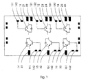
- a compact power semiconductor module in 3-phase bridge topology consists of a base plate, circuit breakers 11-16 and a housing with power and control connections located on the top.
- the circuit breakers are only outlined and not as a number individual power transistors drawn.
- the BOT switch 11 is directly adjacent to the TOP switches 14 of the first phase, as well as the BOT 12 and TOP switches 15 of the second Phase or the BOT-13 and TOP switches 16 of the third phase.
- the gate 111 as well as the Auxiliary emitter terminal 112 of the BOT switch 11 of the first phase is closely adjacent this, as well as the corresponding connections of the other circuit breakers.
- the minus 21, 23, 25 and plus poles 22, 24, 26 of the connections of the DC intermediate circuit are on the first longitudinal side, the 3 phases 31, 32, 33 of AC connections on the second long side.
- the secondary-side components 113 the control circuit including the connections 111, 112 for Power semiconductor module of the BOT switch 11 of the first phase are from the Pulse transformer 1 supplied.
- the pulse transmitter 1 also supplies the secondary side Components 143 of the control circuit including connections 141, 142 for Power semiconductor module of the TOP switch 14.
- the pulse transformer 2 or 3 the corresponding secondary-side component of the second or third phase.
- All crossing points 110, 120, 130, 140 between primary 9 and secondary Lines 8 are the starting points for faults as described above.
- Fig. 3 shows an inventive embodiment of a driver circuit arrangement for direct Mounting on a power semiconductor module according to Fig. 1.
- suitable pulse transmitters 4 on the one hand supplies the secondary side Components 113 of the control circuit of the BOT switch 11 of the first phase.
- This Components 113 are located directly at the control connections 111, 112 for Circuit breaker 11 of the power semiconductor module.
- the pulse transmitter 4 supplies furthermore the secondary-side components 123 of the control circuit of the BOT switch 12 of the second phase. These components 123 are located directly at the Control connections 121, 122 to the power switch 12 of the power semiconductor module.
- the pulse transformer 5 supplies the components 143 on the secondary side Control circuit of the TOP switch 14 of the first phase. These components 143 are located directly at the control connections 141, 142 to the circuit breaker 14 of the Power semiconductor module. Furthermore, the pulse transmitter 4 supplies the secondary side Components 123 of the control circuit of the BOT switch 12 of the second phase. This Components 123 are located directly at the control connections 121, 122 for Circuit breaker 12 of the power semiconductor module.
- the pulse transformer 3 supplies the corresponding ones as in the prior art Third phase device.
- the pulse transmitters 4 or 5 are placed on the secondary-side components 113 and 114, respectively. Because of this Embodiment, the primary-side lines 9 can cross without regard to the 8 lines on the secondary side. Those described in the prior art Disadvantages with regard to crosstalk, interference voltages and Isolation coordination no longer occurs. All lines 8 on the secondary side have one Distance of at least 10mm to the nearest primary line 9. This Increasing the insulation led to the avoidance of voltage flashovers.
- Another advantage of the inventive solution are the large, non-current-carrying ones Surfaces of the printed circuit board of the driver circuit arrangement. These areas are advantageous for Use shielding of the primary cables to each other.
Landscapes
- Engineering & Computer Science (AREA)
- Power Engineering (AREA)
- Power Conversion In General (AREA)
- Electronic Switches (AREA)
Abstract
Description
- Die Anordnung des jeweiligen Impulsübertragers kann nahe an den entsprechenden mit Signalen zu versorgenden Anschlüssen vorgenommen werden. Somit ist ein Kreuzung zwischen primärseitigen und sekundärseitigen Verbindungen verhindert. Daher sind auch die Gefahren durch Übersprechen bzw. Störspannungen auf eine gekreuzte anderen Leitung unterbunden, ein störsicherer Betrieb des Leistungshalbleiterbauelements ist somit gewährleistet.
- Die Abstände der primärseitigen zu den sekundärseitigen Leitungen wird um eine Größenordnung auf 10mm oder mehr erhöht. Damit können die hohen sekundärseitigen Spannungen nicht mehr zu zusätzlich Problemen mit der Isolationskoordination führen, da sämtliche relevanten Strecken deutlich vergrößert wurden.
- Fig. 1
- zeigt das Layout eines Leistungshalbleitermoduls nach dem Stand der Technik.
- Fig. 2
- zeigt eine Treiberschaltungsanordnung für ein Leistungshalbleitermodul nach dem Stand der Technik.
- Fig. 3
- zeigt eine erfinderische Ausgestaltung eine Treiberschaltungsanordnung für ein Leistungshalbleitermodul.
Claims (6)
- Treiberschaltungsanordnung für kompakte Leistungshalbleitermodule in 3- Phasen-Brücken- Topologie bestehend aus mindestens einer Leiterplatte 7 mit aktiven sowie passiven Bauelementen, drei Impulsübertragern 4, 5, 3 für je zwei Ansteuersignale sowie je zwei Spannungsversorgungen sekundärseitiger Bauelemente 113, 123, 133, 143, 153, 163
gekennzeichnet dadurch, dass
sich primärseitige Leitungen 9 nicht mit sekundärseitigen Leitungen 8 kreuzen 110, 120, 130, 140, indem ein erster Impulsübertrager 5 für die beiden TOP- Schalter 14, 15 der ersten sowie zweiten Phase, ein zweiter Impulsübertrager 4 für die beiden BOT-Schalter 11, 12 der ersten sowie der zweiten Phasen und eine dritter Impulsübertrager 3 für den TOP- 16 sowie den BOT- Schalter 13 der dritten Phase eingesetzt wird. - Treiberschaltungsanordnung nach Anspruch 1 dadurch gekennzeichnet, dass der Abstand primärseitiger Leitungen 9 zu sekundärseitigen Leitungen 8 mindestens 10mm beträgt.
- Treiberschaltungsanordnung nach Anspruch 1 dadurch gekennzeichnet, dass die Leistungsschalter 11, 12, 13, 14, 15, 16 Parallelschaltungen von mindestens einem IGBT mit mindestens einer Freilaufdiode sind.
- Treiberschaltungsanordnung nach Anspruch 1 dadurch gekennzeichnet, dass die Leiterplatte 7 direkt oberhalb des Leistungshalbleitermoduls angeordnet ist.
- Treiberschaltungsanordnung nach Anspruch 1 dadurch gekennzeichnet, dass die Impulsübertrager 4, 5, 3 nahe an den sekundärseitigen Bauelemente sowie den Ansteueranschlüssen 111, 112, 121, 122, 131, 132, 141, 142, 151, 152, 161, 162 des Leistungshalbleitermodul angeordnet sind.
- Treiberschaltungsanordnung nach Anspruch 1 dadurch gekennzeichnet, dass anstelle der Impulsübertrager 4, 5, 3 andere Bauelemente, wie Optokoppler oder Levelshifter, zur Pegelanpassung verwendet werden.
Applications Claiming Priority (2)
| Application Number | Priority Date | Filing Date | Title |
|---|---|---|---|
| DE10110100A DE10110100B4 (de) | 2001-03-02 | 2001-03-02 | Schaltungsanordnung für einen Treiber für Leistungsableitermodule |
| DE10110100 | 2001-03-02 |
Publications (3)
| Publication Number | Publication Date |
|---|---|
| EP1237271A2 true EP1237271A2 (de) | 2002-09-04 |
| EP1237271A3 EP1237271A3 (de) | 2008-03-19 |
| EP1237271B1 EP1237271B1 (de) | 2012-02-22 |
Family
ID=7676081
Family Applications (1)
| Application Number | Title | Priority Date | Filing Date |
|---|---|---|---|
| EP01129786A Expired - Lifetime EP1237271B1 (de) | 2001-03-02 | 2001-12-14 | Schaltungdanordnung für einen Treiber für Leistungshalbleitermodule |
Country Status (4)
| Country | Link |
|---|---|
| EP (1) | EP1237271B1 (de) |
| AT (1) | ATE546876T1 (de) |
| DE (1) | DE10110100B4 (de) |
| ES (1) | ES2380592T3 (de) |
Cited By (1)
| Publication number | Priority date | Publication date | Assignee | Title |
|---|---|---|---|---|
| DE102014111438B4 (de) * | 2013-08-12 | 2020-03-26 | Infineon Technologies Ag | Leistungsbaustein und Verfahren zu dessen Herstellung |
Families Citing this family (1)
| Publication number | Priority date | Publication date | Assignee | Title |
|---|---|---|---|---|
| DE10256057B3 (de) * | 2002-11-30 | 2004-05-19 | Semikron Elektronik Gmbh | Schaltungsanordnung zum Schutz eines Transistors gegen Überstrom und Überspannung |
Family Cites Families (4)
| Publication number | Priority date | Publication date | Assignee | Title |
|---|---|---|---|---|
| DE19630173C2 (de) * | 1996-07-26 | 2001-02-08 | Semikron Elektronik Gmbh | Leistungsmodul mit Halbleiterbauelementen |
| DE19781759T1 (de) * | 1997-03-18 | 1999-05-12 | Mitsubishi Electric Corp | Stromrichtereinrichtung |
| DE10037533C1 (de) * | 2000-08-01 | 2002-01-31 | Semikron Elektronik Gmbh | Induktivitätsarme Schaltungsanordnung |
| DE10063714C2 (de) * | 2000-12-20 | 2002-11-07 | Semikron Elektronik Gmbh | Leistungshalbleitermodul mit hoher Isolationsfestigkeit |
-
2001
- 2001-03-02 DE DE10110100A patent/DE10110100B4/de not_active Expired - Fee Related
- 2001-12-14 AT AT01129786T patent/ATE546876T1/de active
- 2001-12-14 ES ES01129786T patent/ES2380592T3/es not_active Expired - Lifetime
- 2001-12-14 EP EP01129786A patent/EP1237271B1/de not_active Expired - Lifetime
Cited By (1)
| Publication number | Priority date | Publication date | Assignee | Title |
|---|---|---|---|---|
| DE102014111438B4 (de) * | 2013-08-12 | 2020-03-26 | Infineon Technologies Ag | Leistungsbaustein und Verfahren zu dessen Herstellung |
Also Published As
| Publication number | Publication date |
|---|---|
| DE10110100A1 (de) | 2002-09-26 |
| ES2380592T3 (es) | 2012-05-16 |
| EP1237271A3 (de) | 2008-03-19 |
| ATE546876T1 (de) | 2012-03-15 |
| EP1237271B1 (de) | 2012-02-22 |
| DE10110100B4 (de) | 2008-03-13 |
Similar Documents
| Publication | Publication Date | Title |
|---|---|---|
| DE102015115271B4 (de) | Elektronikbaugruppe mit entstörkondensatoren und verfahren zum betrieb der elektronikbaugruppe | |
| DE102010002627B4 (de) | Niederinduktive Leistungshalbleiterbaugruppen | |
| DE112016003111B4 (de) | Leistungs-halbleitermodul | |
| EP1178595B1 (de) | Induktivitätsarme Schaltungsanordnung | |
| DE19732402A1 (de) | Elektrische Busanordnung und Verfahren zum Minimieren der Induktanz in einer elektrischen Busanordnung | |
| EP3180850B1 (de) | Niederinduktive schaltungsanordnung eines umrichters | |
| EP2989660B1 (de) | Halbleiterstapel für umrichter mit snubber-kondensatoren | |
| EP2871766B1 (de) | Ansteuerschaltung für Drei-Level-Inverter | |
| DE102004059313B3 (de) | Leistungshalbleitermodul mit verringerten parasitären Induktivitäten | |
| EP3281287B1 (de) | Schnellschaltende schaltungsanordnung für einen umrichter | |
| EP1237271B1 (de) | Schaltungdanordnung für einen Treiber für Leistungshalbleitermodule | |
| DE102014111438B4 (de) | Leistungsbaustein und Verfahren zu dessen Herstellung | |
| EP3621178B1 (de) | Wechselspannungsversorgungseinrichtung | |
| DE102013213986B4 (de) | Dreipunkt-Stromrichter | |
| EP3300470A1 (de) | Umrichter | |
| EP3281289B1 (de) | Leistungsstromrichter mit parallel geschalteten halbleiterschaltern | |
| DE102015105889A1 (de) | Schaltmodul und Umrichter mit wenigstens einem Schaltmodul | |
| EP3304718A1 (de) | Gleichspannungswandler für hohe spannungen | |
| DE102022207268A1 (de) | Inverteranordnung | |
| EP2102977B1 (de) | Schaltungsanordnung zur reduzierten schalterbelastung | |
| WO2017140464A1 (de) | Umrichter | |
| DE102021211519B4 (de) | Elektronische Baugruppe | |
| DE102017205606A1 (de) | Leiterplattenbasismodul für eine leistungselektronische Schaltung | |
| DE102024100740A1 (de) | Inverter, insbesondere mit modular arrangierten Inverterbaugruppen | |
| DE102015210823A1 (de) | Leistungsstromrichter ohne Leistungshalbleitermodul |
Legal Events
| Date | Code | Title | Description |
|---|---|---|---|
| PUAI | Public reference made under article 153(3) epc to a published international application that has entered the european phase |
Free format text: ORIGINAL CODE: 0009012 |
|
| AK | Designated contracting states |
Kind code of ref document: A2 Designated state(s): AT BE CH CY DE DK ES FI FR GB GR IE IT LI LU MC NL PT SE TR |
|
| AX | Request for extension of the european patent |
Free format text: AL;LT;LV;MK;RO;SI |
|
| RAP1 | Party data changed (applicant data changed or rights of an application transferred) |
Owner name: SEMIKRON ELEKTRONIK GMBH & CO. KG |
|
| PUAL | Search report despatched |
Free format text: ORIGINAL CODE: 0009013 |
|
| AK | Designated contracting states |
Kind code of ref document: A3 Designated state(s): AT BE CH CY DE DK ES FI FR GB GR IE IT LI LU MC NL PT SE TR |
|
| AX | Request for extension of the european patent |
Extension state: AL LT LV MK RO SI |
|
| 17P | Request for examination filed |
Effective date: 20080229 |
|
| AKX | Designation fees paid |
Designated state(s): AT BE CH CY DE DK ES FI FR GB GR IE IT LI LU MC NL PT SE TR |
|
| 17Q | First examination report despatched |
Effective date: 20100125 |
|
| GRAP | Despatch of communication of intention to grant a patent |
Free format text: ORIGINAL CODE: EPIDOSNIGR1 |
|
| GRAS | Grant fee paid |
Free format text: ORIGINAL CODE: EPIDOSNIGR3 |
|
| GRAA | (expected) grant |
Free format text: ORIGINAL CODE: 0009210 |
|
| AK | Designated contracting states |
Kind code of ref document: B1 Designated state(s): AT BE CH CY DE DK ES FI FR GB GR IE IT LI LU MC NL PT SE TR |
|
| REG | Reference to a national code |
Ref country code: GB Ref legal event code: FG4D Free format text: NOT ENGLISH |
|
| REG | Reference to a national code |
Ref country code: CH Ref legal event code: EP |
|
| REG | Reference to a national code |
Ref country code: CH Ref legal event code: NV Representative=s name: BRAUNPAT BRAUN EDER AG Ref country code: AT Ref legal event code: REF Ref document number: 546876 Country of ref document: AT Kind code of ref document: T Effective date: 20120315 |
|
| REG | Reference to a national code |
Ref country code: IE Ref legal event code: FG4D Free format text: LANGUAGE OF EP DOCUMENT: GERMAN |
|
| REG | Reference to a national code |
Ref country code: DE Ref legal event code: R096 Ref document number: 50116060 Country of ref document: DE Effective date: 20120419 |
|
| REG | Reference to a national code |
Ref country code: ES Ref legal event code: FG2A Ref document number: 2380592 Country of ref document: ES Kind code of ref document: T3 Effective date: 20120516 |
|
| REG | Reference to a national code |
Ref country code: NL Ref legal event code: VDEP Effective date: 20120222 |
|
| PG25 | Lapsed in a contracting state [announced via postgrant information from national office to epo] |
Ref country code: NL Free format text: LAPSE BECAUSE OF FAILURE TO SUBMIT A TRANSLATION OF THE DESCRIPTION OR TO PAY THE FEE WITHIN THE PRESCRIBED TIME-LIMIT Effective date: 20120222 |
|
| PG25 | Lapsed in a contracting state [announced via postgrant information from national office to epo] |
Ref country code: FI Free format text: LAPSE BECAUSE OF FAILURE TO SUBMIT A TRANSLATION OF THE DESCRIPTION OR TO PAY THE FEE WITHIN THE PRESCRIBED TIME-LIMIT Effective date: 20120222 Ref country code: PT Free format text: LAPSE BECAUSE OF FAILURE TO SUBMIT A TRANSLATION OF THE DESCRIPTION OR TO PAY THE FEE WITHIN THE PRESCRIBED TIME-LIMIT Effective date: 20120622 Ref country code: GR Free format text: LAPSE BECAUSE OF FAILURE TO SUBMIT A TRANSLATION OF THE DESCRIPTION OR TO PAY THE FEE WITHIN THE PRESCRIBED TIME-LIMIT Effective date: 20120523 |
|
| REG | Reference to a national code |
Ref country code: IE Ref legal event code: FD4D |
|
| PG25 | Lapsed in a contracting state [announced via postgrant information from national office to epo] |
Ref country code: CY Free format text: LAPSE BECAUSE OF FAILURE TO SUBMIT A TRANSLATION OF THE DESCRIPTION OR TO PAY THE FEE WITHIN THE PRESCRIBED TIME-LIMIT Effective date: 20120222 |
|
| PG25 | Lapsed in a contracting state [announced via postgrant information from national office to epo] |
Ref country code: DK Free format text: LAPSE BECAUSE OF FAILURE TO SUBMIT A TRANSLATION OF THE DESCRIPTION OR TO PAY THE FEE WITHIN THE PRESCRIBED TIME-LIMIT Effective date: 20120222 Ref country code: SE Free format text: LAPSE BECAUSE OF FAILURE TO SUBMIT A TRANSLATION OF THE DESCRIPTION OR TO PAY THE FEE WITHIN THE PRESCRIBED TIME-LIMIT Effective date: 20120222 Ref country code: IE Free format text: LAPSE BECAUSE OF FAILURE TO SUBMIT A TRANSLATION OF THE DESCRIPTION OR TO PAY THE FEE WITHIN THE PRESCRIBED TIME-LIMIT Effective date: 20120222 |
|
| PG25 | Lapsed in a contracting state [announced via postgrant information from national office to epo] |
Ref country code: IT Free format text: LAPSE BECAUSE OF FAILURE TO SUBMIT A TRANSLATION OF THE DESCRIPTION OR TO PAY THE FEE WITHIN THE PRESCRIBED TIME-LIMIT Effective date: 20120222 |
|
| PLBE | No opposition filed within time limit |
Free format text: ORIGINAL CODE: 0009261 |
|
| STAA | Information on the status of an ep patent application or granted ep patent |
Free format text: STATUS: NO OPPOSITION FILED WITHIN TIME LIMIT |
|
| 26N | No opposition filed |
Effective date: 20121123 |
|
| REG | Reference to a national code |
Ref country code: DE Ref legal event code: R097 Ref document number: 50116060 Country of ref document: DE Effective date: 20121123 |
|
| BERE | Be: lapsed |
Owner name: SEMIKRON ELEKTRONIK G.M.B.H. & CO. KG Effective date: 20121231 |
|
| PG25 | Lapsed in a contracting state [announced via postgrant information from national office to epo] |
Ref country code: MC Free format text: LAPSE BECAUSE OF NON-PAYMENT OF DUE FEES Effective date: 20121231 |
|
| PG25 | Lapsed in a contracting state [announced via postgrant information from national office to epo] |
Ref country code: BE Free format text: LAPSE BECAUSE OF NON-PAYMENT OF DUE FEES Effective date: 20121231 |
|
| REG | Reference to a national code |
Ref country code: AT Ref legal event code: MM01 Ref document number: 546876 Country of ref document: AT Kind code of ref document: T Effective date: 20121214 |
|
| PG25 | Lapsed in a contracting state [announced via postgrant information from national office to epo] |
Ref country code: TR Free format text: LAPSE BECAUSE OF FAILURE TO SUBMIT A TRANSLATION OF THE DESCRIPTION OR TO PAY THE FEE WITHIN THE PRESCRIBED TIME-LIMIT Effective date: 20120222 |
|
| PG25 | Lapsed in a contracting state [announced via postgrant information from national office to epo] |
Ref country code: AT Free format text: LAPSE BECAUSE OF NON-PAYMENT OF DUE FEES Effective date: 20121214 Ref country code: LU Free format text: LAPSE BECAUSE OF NON-PAYMENT OF DUE FEES Effective date: 20121214 |
|
| REG | Reference to a national code |
Ref country code: FR Ref legal event code: PLFP Year of fee payment: 15 |
|
| REG | Reference to a national code |
Ref country code: FR Ref legal event code: PLFP Year of fee payment: 16 |
|
| PGFP | Annual fee paid to national office [announced via postgrant information from national office to epo] |
Ref country code: CH Payment date: 20161222 Year of fee payment: 16 Ref country code: GB Payment date: 20161222 Year of fee payment: 16 |
|
| PGFP | Annual fee paid to national office [announced via postgrant information from national office to epo] |
Ref country code: ES Payment date: 20161221 Year of fee payment: 16 Ref country code: FR Payment date: 20161221 Year of fee payment: 16 |
|
| PGFP | Annual fee paid to national office [announced via postgrant information from national office to epo] |
Ref country code: DE Payment date: 20161231 Year of fee payment: 16 |
|
| REG | Reference to a national code |
Ref country code: CH Ref legal event code: PCAR Free format text: NEW ADDRESS: HOLEESTRASSE 87, 4054 BASEL (CH) |
|
| REG | Reference to a national code |
Ref country code: DE Ref legal event code: R119 Ref document number: 50116060 Country of ref document: DE |
|
| REG | Reference to a national code |
Ref country code: CH Ref legal event code: PL |
|
| GBPC | Gb: european patent ceased through non-payment of renewal fee |
Effective date: 20171214 |
|
| REG | Reference to a national code |
Ref country code: FR Ref legal event code: ST Effective date: 20180831 |
|
| PG25 | Lapsed in a contracting state [announced via postgrant information from national office to epo] |
Ref country code: DE Free format text: LAPSE BECAUSE OF NON-PAYMENT OF DUE FEES Effective date: 20180703 Ref country code: FR Free format text: LAPSE BECAUSE OF NON-PAYMENT OF DUE FEES Effective date: 20180102 |
|
| PG25 | Lapsed in a contracting state [announced via postgrant information from national office to epo] |
Ref country code: GB Free format text: LAPSE BECAUSE OF NON-PAYMENT OF DUE FEES Effective date: 20171214 Ref country code: LI Free format text: LAPSE BECAUSE OF NON-PAYMENT OF DUE FEES Effective date: 20171231 Ref country code: CH Free format text: LAPSE BECAUSE OF NON-PAYMENT OF DUE FEES Effective date: 20171231 |
|
| REG | Reference to a national code |
Ref country code: ES Ref legal event code: FD2A Effective date: 20190703 |
|
| PG25 | Lapsed in a contracting state [announced via postgrant information from national office to epo] |
Ref country code: ES Free format text: LAPSE BECAUSE OF NON-PAYMENT OF DUE FEES Effective date: 20171215 |