EP1237271A2 - Circuit arrangement for a driver for power semiconductor module - Google Patents
Circuit arrangement for a driver for power semiconductor module Download PDFInfo
- Publication number
- EP1237271A2 EP1237271A2 EP01129786A EP01129786A EP1237271A2 EP 1237271 A2 EP1237271 A2 EP 1237271A2 EP 01129786 A EP01129786 A EP 01129786A EP 01129786 A EP01129786 A EP 01129786A EP 1237271 A2 EP1237271 A2 EP 1237271A2
- Authority
- EP
- European Patent Office
- Prior art keywords
- power semiconductor
- circuit arrangement
- driver circuit
- pulse
- semiconductor module
- Prior art date
- Legal status (The legal status is an assumption and is not a legal conclusion. Google has not performed a legal analysis and makes no representation as to the accuracy of the status listed.)
- Granted
Links
Images

Classifications
-
- H—ELECTRICITY
- H02—GENERATION; CONVERSION OR DISTRIBUTION OF ELECTRIC POWER
- H02M—APPARATUS FOR CONVERSION BETWEEN AC AND AC, BETWEEN AC AND DC, OR BETWEEN DC AND DC, AND FOR USE WITH MAINS OR SIMILAR POWER SUPPLY SYSTEMS; CONVERSION OF DC OR AC INPUT POWER INTO SURGE OUTPUT POWER; CONTROL OR REGULATION THEREOF
- H02M7/00—Conversion of AC power input into DC power output; Conversion of DC power input into AC power output
- H02M7/003—Constructional details, e.g. physical layout, assembly, wiring or busbar connections
-
- H—ELECTRICITY
- H03—ELECTRONIC CIRCUITRY
- H03K—PULSE TECHNIQUE
- H03K17/00—Electronic switching or gating, i.e. not by contact-making and –breaking
- H03K17/16—Modifications for eliminating interference voltages or currents
Definitions
- the invention describes a driver circuit arrangement for a power semiconductor module in the topology of a 3-phase bridge according to the preamble of claim 1.
- driver circuitry for power semiconductor modules are from the literature known. In increasing the performance as well as increasing the Reliability of the power semiconductor modules is an optimization of the used ones Driver circuitry an imperative.
- a compact arrangement of the power semiconductor module and associated Driver circuit arrangement can be realized by this directly on the Power semiconductor module is arranged. Such an arrangement forces the Driver circuit a certain topology of their drive connections to the Power semiconductor module on.
- the task of the driver circuit is to control the circuit breakers after one by e.g. a microprocessor predetermined switching pattern such that the Output voltage of the power semiconductor module one for the respective application ideal output voltage corresponds as far as possible.
- the Driver circuit arrangement from a variety of active and passive components.
- Optocouplers Essentially two types of components are used for level adjustment, on the one hand optocouplers, on the other hand pulse transmitters. Have opposite pulse transmitters Optocouplers also have the advantage of being able to transmit power and thus as Power supply for components on the secondary side of level adjustment to be able to serve.
- the prior art includes pulse transmitters with two control channels for transmission of two control signals, each for a TOP and a BOT switch as well two secondary supply channels for power supply on the secondary side Consumer.
- Such consumers are exemplary components for correcting the Signal form of the transmitted control signals.
- transformers Signals such as Error signals, transmitted from the secondary to the primary side.
- Prior art driver circuitry assigns each phase to a 3-phase Bridge circuit to a pulse transformer.
- the invention has for its object a circuit arrangement for a Driver circuit arrangement for driving a power semiconductor module in the Topology of a 3-phase bridge with increased interference immunity and high Quality of insulation coordination with safe electrical isolation and high reliability imagine.
- Compact power semiconductor modules in 3-phase bridge topology have special features constructive conditions, since they are exemplary on particularly low parasitic Inductors are designed.
- State of the art are power semiconductor modules with the the base plate, usually a ceramic substrate, facing away from the side Power and control connections.
- the DC connections are one of the two long sides, the three AC connections on the opposite.
- the Most of the control connections are also located on the long sides of the Power semiconductor module. These are typically the gate and the Auxiliary emitter terminals.
- the control connections are located in this topology the BOT switch on one side, the TOP switch on the one opposite.
- the circuit board of the driver circuit arrangement is located directly above this Control connections on the power semiconductor module. With this arrangement you can short connections between the power semiconductor module and the Driver circuitry can be realized.
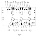
- a compact power semiconductor module in 3-phase bridge topology consists of a base plate, circuit breakers 11-16 and a housing with power and control connections located on the top.
- the circuit breakers are only outlined and not as a number individual power transistors drawn.
- the BOT switch 11 is directly adjacent to the TOP switches 14 of the first phase, as well as the BOT 12 and TOP switches 15 of the second Phase or the BOT-13 and TOP switches 16 of the third phase.
- the gate 111 as well as the Auxiliary emitter terminal 112 of the BOT switch 11 of the first phase is closely adjacent this, as well as the corresponding connections of the other circuit breakers.
- the minus 21, 23, 25 and plus poles 22, 24, 26 of the connections of the DC intermediate circuit are on the first longitudinal side, the 3 phases 31, 32, 33 of AC connections on the second long side.
- the secondary-side components 113 the control circuit including the connections 111, 112 for Power semiconductor module of the BOT switch 11 of the first phase are from the Pulse transformer 1 supplied.
- the pulse transmitter 1 also supplies the secondary side Components 143 of the control circuit including connections 141, 142 for Power semiconductor module of the TOP switch 14.
- the pulse transformer 2 or 3 the corresponding secondary-side component of the second or third phase.
- All crossing points 110, 120, 130, 140 between primary 9 and secondary Lines 8 are the starting points for faults as described above.
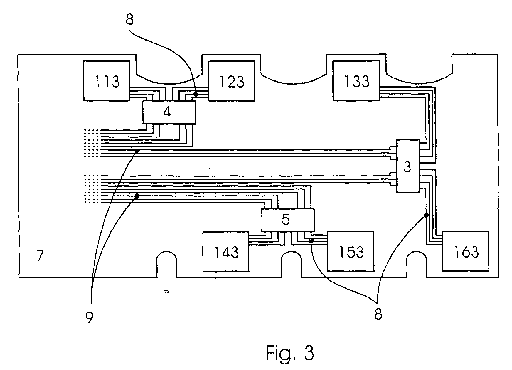
- Fig. 3 shows an inventive embodiment of a driver circuit arrangement for direct Mounting on a power semiconductor module according to Fig. 1.
- suitable pulse transmitters 4 on the one hand supplies the secondary side Components 113 of the control circuit of the BOT switch 11 of the first phase.
- This Components 113 are located directly at the control connections 111, 112 for Circuit breaker 11 of the power semiconductor module.
- the pulse transmitter 4 supplies furthermore the secondary-side components 123 of the control circuit of the BOT switch 12 of the second phase. These components 123 are located directly at the Control connections 121, 122 to the power switch 12 of the power semiconductor module.
- the pulse transformer 5 supplies the components 143 on the secondary side Control circuit of the TOP switch 14 of the first phase. These components 143 are located directly at the control connections 141, 142 to the circuit breaker 14 of the Power semiconductor module. Furthermore, the pulse transmitter 4 supplies the secondary side Components 123 of the control circuit of the BOT switch 12 of the second phase. This Components 123 are located directly at the control connections 121, 122 for Circuit breaker 12 of the power semiconductor module.
- the pulse transformer 3 supplies the corresponding ones as in the prior art Third phase device.
- the pulse transmitters 4 or 5 are placed on the secondary-side components 113 and 114, respectively. Because of this Embodiment, the primary-side lines 9 can cross without regard to the 8 lines on the secondary side. Those described in the prior art Disadvantages with regard to crosstalk, interference voltages and Isolation coordination no longer occurs. All lines 8 on the secondary side have one Distance of at least 10mm to the nearest primary line 9. This Increasing the insulation led to the avoidance of voltage flashovers.
- Another advantage of the inventive solution are the large, non-current-carrying ones Surfaces of the printed circuit board of the driver circuit arrangement. These areas are advantageous for Use shielding of the primary cables to each other.
Landscapes
- Engineering & Computer Science (AREA)
- Power Engineering (AREA)
- Power Conversion In General (AREA)
- Electronic Switches (AREA)
Abstract
Die Erfindung beschreibt eine Treiberschaltung für kompakte Leistungshalbleitermodule in
3- Phasen- Brücken- Topologie Bei der Erhöhung der Leistungsfähigkeit sowie einer
Steigerung der Zuverlässigkeit derartiger Leistungshalbleitermodule ist eine Optimierung
der verwendeten Treiberschaltung eine zwingende Voraussetzung. Diese
Treiberschaltungen bestehen in der Regel aus einer Leiterplatte 7 mit aktiven sowie
passiven Bauelementen, drei Impulsübertragern 4, 5, 3 für je zwei Ansteuersignale sowie
zwei Spannungsversorgungen sekundärseitiger Bauelemente 113, 123, 133, 143, 153, 163.
Die Topologie der erfinderischen Treiberschaltungen ist gekennzeichnet durch einen ersten
Impulsübertrager 5 für die beiden TOP- Schalter 14, 15 der ersten sowie zweiten Phase,
einen zweiten Impulsübertrager 4 für die beiden BOT- Schalter 11, 12 der ersten sowie der
zweiten Phasen und einen dritten Impulsübertrager 3 für den TOP- 16 sowie den BOT-Schalter
13 der dritten. Dadurch ist eine gewährleistet, dass sich primärseitige nicht mit
sekundärseitigen Leitungen kreuzen.
Description
Die Erfindung beschreibt eine Treiberschaltungsanordnung für ein Leistungshalbleitermodul in der Topologie einer 3- Phasen Brücke nach dem Oberbegriff des Anspruches 1. Derartige Treiberschaltungsanordnung für Leistungshalbleitermodule sind aus der Literatur bekannt. Bei der Erhöhung der Leistungsfähigkeit sowie einer Steigerung der Zuverlässigkeit der Leistungshalbleitermodule ist eine Optimierung der verwendeten Treiberschaltungsanordnung eine zwingende Voraussetzung.The invention describes a driver circuit arrangement for a power semiconductor module in the topology of a 3-phase bridge according to the preamble of claim 1. Such driver circuitry for power semiconductor modules are from the literature known. In increasing the performance as well as increasing the Reliability of the power semiconductor modules is an optimization of the used ones Driver circuitry an imperative.
In der Entwicklung von Leistungshalbleitermodulen bilden den modernen Stand der Technik kompakte Aufbauvarianten, die beispielsweise einen 3- Phasen- Brückengleichrichter in einem Gehäuse ohne Grundplatte vereinen. Derartige Aufbauten sind beispielhaft aus der DE 196 30 173 C1 bekannt. Weitere aktuelle Entwicklungen betreffen die Verringerung der parasitären Induktivitäten in Leistungshalbleitermodulen, wie beispielhaft in der DE 100 37 533 A1 vorgestellt. Die Entwicklung der in derartigen Modulen eingesetzten Leistungsschalter, die vornehmlich aus einer Parallelschaltung von mehreren Leistungstransistoren wie z.B. IGBTs (insulated gate bipolar transistor) mit parallel geschalteten Freilaufdioden bestehen, geht zu höheren Sperrspannungen. Den Stand der Technik bilden hier IGBTs der Sperrspannungsklassen 600V, 1200V, 1700V sowie 3300V.In the development of power semiconductor modules form the modern state of the art compact design variants, for example in a 3-phase bridge rectifier combine in a housing without a base plate. Such structures are exemplary from the DE 196 30 173 C1 known. Further current developments concern the reduction of parasitic inductances in power semiconductor modules, such as in the DE 100 37 533 A1 presented. The development of those used in such modules Circuit breakers, which consist primarily of a parallel connection of several Power transistors such as IGBTs (insulated gate bipolar transistor) with parallel switched freewheeling diodes exist, goes to higher reverse voltages. The state of the Technology forms IGBTs of the blocking voltage classes 600V, 1200V, 1700V and 3300V.
Durch derartige kompakte Module mit steigender Leistungsfähigkeit bei verringertem Flächenbedarf steigen auch die Anforderungen an die zu ihrer Ansteuerung benötigten Treiberschaltungen.Through such compact modules with increasing performance with reduced Space requirements also increase the requirements for those required to control them Driver circuits.
Eine kompakte Anordnung aus Leistungshalbleitermodul und dazugehöriger Treiberschaltungsanordnung ist realisierbar indem diese direkt auf dem Leistungshalbleitermodul angeordnet ist. Eine derartige Anordnung zwingt der Treiberschaltung eine gewisse Topologie ihrer Ansteueranschlüsse an das Leistungshalbleitermodul auf.A compact arrangement of the power semiconductor module and associated Driver circuit arrangement can be realized by this directly on the Power semiconductor module is arranged. Such an arrangement forces the Driver circuit a certain topology of their drive connections to the Power semiconductor module on.
Die Aufgabe der Treiberschaltung besteht in der Ansteuerung der Leistungsschaltern nach einem durch z.B. einen Mikroprozessor vorgegebenen Schaltmuster derart, dass die Ausgangsspannung des Leistungshalbleitermoduls einer für den jeweiligen Einsatzzweck idealen Ausgangsspannung weitestgehend entspricht. Zu diesem Zweck besteht die Treiberschaltungsanordnung aus eine Vielzahl aktiver sowie passiver Bauelemente.The task of the driver circuit is to control the circuit breakers after one by e.g. a microprocessor predetermined switching pattern such that the Output voltage of the power semiconductor module one for the respective application ideal output voltage corresponds as far as possible. For this purpose the Driver circuit arrangement from a variety of active and passive components.
Eine wesentlich Rolle kommt bei der genannten Aufgabe der Pegelanpassung der Ansteuersignale der Leistungsschalter zu. Diese Pegelanpassung ist in der Regel sowohl für die TOP- Schalter als auch für die BOT- Schalter einer 3- Phasen- Brückenschaltung notwendig, da das Bezugspotential auch für die BOT- Schalter nicht zwangsläufig identisch ist mit dem Bezugspotential der Treiberschaltungsanordnung.An essential role comes in the mentioned task of level adjustment Control signals of the circuit breakers. This level adjustment is usually both for the TOP switches as well as for the BOT switches of a 3-phase bridge circuit This is necessary because the reference potential is not necessarily identical for the BOT switches either is with the reference potential of the driver circuit arrangement.
Als Pegelanpassung kommen im wesentliche zwei Arten von Bauelement zum Einsatz, einerseits Optokoppler, anderseits Impulsübertrager. Impulsübertrager haben gegenüber Optokoppplern den Vorteil auch Leistung übertragen zu können und somit als Spannungsversorgung von Bauelemente auf der Sekundärseite der Pegelanpassung dienen zu können.Essentially two types of components are used for level adjustment, on the one hand optocouplers, on the other hand pulse transmitters. Have opposite pulse transmitters Optocouplers also have the advantage of being able to transmit power and thus as Power supply for components on the secondary side of level adjustment to be able to serve.
Zum Stand der Technik zählen Impulsübertrager mit zwei Steuerkanälen zur Übertragung von zwei Ansteuersignalen beispielhaft für je einen TOP- und einen BOT- Schalters sowie zwei sekundärseitigen Versorgungskanälen zur Spannungsversorgung sekundärseitiger Verbraucher. Derartige Verbraucher sind beispielhaft Bauelemente zur Korrektur der Signalform der übertragenen Ansteuersignale. Weiterhin können derartige Übertrager Signale, wie z.B. Fehlersignale, von der Sekundär- auf die Primärseite übertragen.The prior art includes pulse transmitters with two control channels for transmission of two control signals, each for a TOP and a BOT switch as well two secondary supply channels for power supply on the secondary side Consumer. Such consumers are exemplary components for correcting the Signal form of the transmitted control signals. Furthermore, such transformers Signals such as Error signals, transmitted from the secondary to the primary side.
Treiberschaltungsanordnungen nach dem Stand der Technik ordnen jeder Phase einer 3-Phasen- Brückenschaltung einen Impulsübertrager zu.Prior art driver circuitry assigns each phase to a 3-phase Bridge circuit to a pulse transformer.
Dabei kommt es zwangsläufig zu Topologien bei denen primärseitige Signalwege von sekundärseitigen gekreuzt werden. An derartigen Kreuzungspunkten ist der Abstand zwischen den beiden sich kreuzenden Leitungen bei Verwendung gängiger Leitplatten in der Größenordnung von 1mm oder weniger.This inevitably leads to topologies in which primary signal paths from are crossed on the secondary side. The distance is at such crossing points between the two crossing lines when using common baffles in on the order of 1mm or less.
Besonders bei Verwendung von IGBTs der Sperrspannungsklassen über 600V sind kurze Schaltzeiten der Leistungsschalter zur Erzeugung qualitativ hochwertiger Ausgangssignale des Leistungshalbleitermoduls notwendig. Dieses schnelle Schalten entspricht schnellen Spannungsänderungen (hohes dU/dt) auf den Ansteuerleitungen.Especially when using IGBTs of reverse voltage classes over 600V are short Switching times of the circuit breakers to generate high quality output signals of the power semiconductor module is necessary. This fast switching corresponds to fast Voltage changes (high dU / dt) on the control lines.
Derartige schnelle Spannungsänderungen können an den Knotenpunkten zu Übersprechen bzw. Störspannungen auf der jeweils anderen Leitung führen. Diese Störspannungen können zu Störungen im Betrieb des Leistunghalbleitermoduls oder sogar zu dessen Ausfall führen.Such rapid voltage changes can lead to crosstalk at the nodes or lead to interference voltages on the other line. These interference voltages can lead to malfunctions in the operation of the power semiconductor module or even to it Failure.
Die hohen sekundärseitigen Spannungen führen zusätzlich zu Problemen mit der Isolationskoordination. Hierunter werden Effekte wie Teilentladungen im Volumen und an der Oberfläche der Leiterplatte verstanden. Weitergehende Informationen hierzu finden sich in "Kapitel 1 bei König, Rao, Teilentladungen in Betriebsmitteln der Energietechnik, VDE-Verlag 1993 ISBN 3-8007-1764-6", in der DIN EN 50178 (VDE 0160) sowie bezüglich der Auswirkungen auf Leistungshalbleiterbauelemente in der DE 100 63 714 A1.The high secondary voltages also lead to problems with the Insulation coordination. This includes effects such as partial discharges in volume and on understood the surface of the circuit board. Further information can be found in "Chapter 1 at König, Rao, partial discharges in energy technology equipment, VDE publishing house 1993 ISBN 3-8007-1764-6 ", in DIN EN 50178 (VDE 0160) and with regard to Effects on power semiconductor components in DE 100 63 714 A1.
Der Erfindung liegt die Aufgabe zugrunde eine Schaltungsanordnung für eine Treiberschaltungsanordnung zur Ansteuerung eines Leistungshalbleitermoduls in der Topologie einer 3- Phasen- Brücke mit gesteigerter Störspannungsfestigkeit sowie hoher Qualität der Isolationskoordination bei sicherer Potentialtrennung und hoher Zuverlässigkeit vorzustellen.The invention has for its object a circuit arrangement for a Driver circuit arrangement for driving a power semiconductor module in the Topology of a 3-phase bridge with increased interference immunity and high Quality of insulation coordination with safe electrical isolation and high reliability imagine.
Die Aufgabe wird erfindungsgemäß gelöst durch die Merkmale des kennzeichnenden Teils des Anspruchs 1. Bevorzugte Ausführungsformen sind in den Unteransprüchen beschrieben.The object is achieved by the features of the characterizing part of claim 1. Preferred embodiments are in the subclaims described.
Kompakte Leistungshalbleitermodule in 3- Phasen- Brücken- Topologie weisen spezielle konstruktive Gegebenheiten auf, da sie beispielhaft auf besonders geringe parasitäre Induktivitäten ausgelegt sind. Stand der Technik sind Leistungshalbleitermodule mit an der der Grundplatte, meist einem keramischen Substrat, abgewandten Seite herausgeführten Leistungs- sowie Ansteueranschlüssen. Durch den inneren Aufbau dieser Leistungshalbleitermodule vorgegeben befinden sich die Gleichstromanschlüsse ein einer der beiden Längsseiten, die drei Wechselstromanschlüsse an der gegenüberliegenden. Die Mehrzahl der Ansteueranschlüsse befindet sich ebenfalls an den Längsseiten des Leistungshalbleitermoduls. Hierbei handelt es sich typischerweise um die Gate- sowie die Hilfsemitteranschlüsse. Bei dieser Aufbautopologie befinden sich die Ansteueranschlüsse der BOT- Schalter auf der einen Seite, diejenigen der TOP- Schalter auf der gegenüberliegenden. Compact power semiconductor modules in 3-phase bridge topology have special features constructive conditions, since they are exemplary on particularly low parasitic Inductors are designed. State of the art are power semiconductor modules with the the base plate, usually a ceramic substrate, facing away from the side Power and control connections. Through the internal structure of this Given power semiconductor modules, the DC connections are one of the two long sides, the three AC connections on the opposite. The Most of the control connections are also located on the long sides of the Power semiconductor module. These are typically the gate and the Auxiliary emitter terminals. The control connections are located in this topology the BOT switch on one side, the TOP switch on the one opposite.
Die Leiterplatte der Treiberschaltungsanordnung befindet sich direkt oberhalb diese Ansteueranschlüsse auf dem Leistungshalbleitermodul. Durch diese Anordnung können kurze Verbindungen zwischen dem Leistungshalbleitermodul und der Treiberschaltungsanordnung realisiert werden.The circuit board of the driver circuit arrangement is located directly above this Control connections on the power semiconductor module. With this arrangement you can short connections between the power semiconductor module and the Driver circuitry can be realized.
Die jeder der drei Phasen und somit je einem TOP- sowie einem BOT- Schalter zugeordneten Impulsübertrager befinden sich bei dieser Topologie zwischen den jeweiligen Anschlüssen auf der Leiterplatte der Treiberschaltungsanordnung. Daher ergeben sich zwangsläufig Kreuzungspunkte zwischen primärseitigen und sekundärseitigen Signalen.The each of the three phases and thus one TOP and one BOT switch assigned pulse transmitters are in this topology between the respective Connections on the printed circuit board of the driver circuit arrangement. Hence arise inevitably crossing points between primary and secondary signals.
Die Erfinderische Ausgestaltung der Leiterplatte der Treiberschaltungsanordnung verwendet für eine erste sowie eine zweite Phase des Wechselstroms zwei Übertrager in einer Zuordnung derart, dass die beiden TOP- Schalter der ersten und zweiten Phase einem ersten Impulsübertrager zugeordnet sind sowie die beiden BOT- Schalter der ersten und zweiten Phase einem zweiten Impulsübertrager zugeordnet sind. Die Zuordnung des dritten Impulsübertrager bleibt gegenüber dem Stand der Technik unverändert. Die Zuordnung des ersten bzw. zweiten Impulsübertragers zu den TOP- bzw. BOT- Schaltern der ersten und zweiten Phase weist folgende erfinderisch Vorteile gegenüber dem Stand der Technik auf:
- Die Anordnung des jeweiligen Impulsübertragers kann nahe an den entsprechenden mit Signalen zu versorgenden Anschlüssen vorgenommen werden. Somit ist ein Kreuzung zwischen primärseitigen und sekundärseitigen Verbindungen verhindert. Daher sind auch die Gefahren durch Übersprechen bzw. Störspannungen auf eine gekreuzte anderen Leitung unterbunden, ein störsicherer Betrieb des Leistungshalbleiterbauelements ist somit gewährleistet.
- Die Abstände der primärseitigen zu den sekundärseitigen Leitungen wird um eine Größenordnung auf 10mm oder mehr erhöht. Damit können die hohen sekundärseitigen Spannungen nicht mehr zu zusätzlich Problemen mit der Isolationskoordination führen, da sämtliche relevanten Strecken deutlich vergrößert wurden.
- The arrangement of the respective pulse transmitter can be carried out close to the corresponding connections to be supplied with signals. This prevents the primary and secondary connections from crossing. Therefore, the dangers of crosstalk or interference voltages on a crossed other line are prevented, an interference-free operation of the power semiconductor component is thus guaranteed.
- The distances between the primary-side and the secondary-side lines are increased by an order of magnitude to 10 mm or more. As a result, the high voltages on the secondary side can no longer lead to additional problems with insulation coordination, since all relevant routes have been significantly enlarged.
Dieser deutlichen Gewinn an Zuverlässigkeit der Treiberschaltungsanordnung führt auch direkt zu einer der Erhöhung der Leistungsfähigkeit sowie einer Steigerung der Zuverlässigkeit des Systems aus Leistungshalbleitermodul und der zugehörigen Treiberschaltungsanordnung. This significant gain in reliability of the driver circuitry also leads directly to an increase in performance as well as an increase in Reliability of the system comprising the power semiconductor module and the associated one Drive circuitry.
Der erfinderisch Gedanke wird anhand der Ausführungsbeispiele in den Fig. 1 bis 3 näher erläutert.
- Fig. 1
- zeigt das Layout eines Leistungshalbleitermoduls nach dem Stand der Technik.
- Fig. 2
- zeigt eine Treiberschaltungsanordnung für ein Leistungshalbleitermodul nach dem Stand der Technik.
- Fig. 3
- zeigt eine erfinderische Ausgestaltung eine Treiberschaltungsanordnung für ein Leistungshalbleitermodul.
- Fig. 1
- shows the layout of a power semiconductor module according to the prior art.
- Fig. 2
- shows a driver circuit arrangement for a power semiconductor module according to the prior art.
- Fig. 3
- shows an inventive embodiment of a driver circuit arrangement for a power semiconductor module.
Ein kompaktes Leistungshalbleitermodul in 3- Phasen- Brücken- Topologie nach Fig. 1
besteht neben einer Grundplatte, aus den Leistungsschaltern 11-16 sowie einem Gehäuse
mit an dessen Oberseite befindlichen Leistungs- und Ansteueranschlüssen. Der
Übersichlichkeit halber sind die Leistungsschalter nur skizziert und nicht als eine Anzahl
einzelner Leistungstransistoren gezeichnet. Der BOT- Schalter 11 ist direkt benachbart zum
TOP- Schalter 14 der ersten Phase, ebenso die BOT- 12 und TOP- Schalter 15 der zweiten
Phase bzw. die BOT- 13 und TOP- Schalter 16 der dritten Phase. Der Gate- 111 sowie der
Hilfsemitteranschluss 112 des BOT- Schalters 11 der ersten Phase liegt eng benachbart zu
diesem, ebenso die entsprechenden Anschlüsse der anderen Leistungsschalter.A compact power semiconductor module in 3-phase bridge topology according to FIG. 1
consists of a base plate, circuit breakers 11-16 and a housing
with power and control connections located on the top. The
For the sake of clarity, the circuit breakers are only outlined and not as a number
individual power transistors drawn. The
Die Minus- 21, 23, 25 sowie Pluspole 22, 24 ,26 der Anschlüsse des
Gleichstromzwischenkreises liegen an der ersten Längsseite die 3 Phasen 31, 32, 33 der
Wechselstromanschlüsse an der zweiten Längsseite. Auf die Darstellung der internen
Verschaltung wurde verzichtet.The minus 21, 23, 25 and
Fig. 2 zeigt den Stand der Technik einer Treiberschaltungsanordnung zur direkten Montage
auf einem Leistungshalbleitermodul nach Fig. 1. Die sekundärseitigen Bauelemente 113
der Ansteuerschaltung einschließlich der Anschlüsse 111, 112 zum
Leistungshalbleitermodul des BOT- Schalters 11 der ersten Phase werden aus dem
Impulsübertrager 1 versorgt. Der Impulsübertrager 1 versorgt ebenso die sekundärseitigen
Bauelemente 143 der Ansteuerschaltung einschließlich der Anschlüsse 141, 142 zum
Leistungshalbleitermodul des TOP- Schalters 14. Analog versorgt der Impulsübertrager 2
bzw. 3 die entsprechenden sekundärseitigen Bauelement der zweiten bzw. dritten Phase.2 shows the prior art of a driver circuit arrangement for direct assembly
on a power semiconductor module according to FIG. 1. The secondary-
Alle Kreuzungspunkte 110, 120, 130, 140 zwischen primärseitigen 9 und sekundärseitigen
Leitungen 8 sind die Ausgangspunkte für Störungen wie oben beschrieben. All crossing points 110, 120, 130, 140 between primary 9 and
Fig. 3 zeigt eine erfinderische Ausgestaltung einer Treiberschaltungsanordnung zur direkten
Montage auf einem Leistungshalbleitermodul nach Fig. 1. Der für die Versorgung von zwei
Leistungschaltern geeignete Impulsübertrager 4 versorgt einerseits die sekundärseitigen
Bauelemente 113 der Ansteuerschaltung des BOT- Schalters 11 der ersten Phase. Diese
Bauelemente 113 befinden sich direkt bei den Ansteueranschlüssen 111, 112 zum
Leistungsschalters 11 des Leistungshalbleitermoduls. Der Impulsübertrager 4 versorgt
weiterhin die sekundärseitigen Bauelemente 123 der Ansteuerschaltung des BOT-Schalters
12 der zweiten Phase. Diese Bauelemente 123 befinden sich direkt bei den
Ansteueranschlüssen 121, 122 zum Leistungsschalters 12 des Leistungshalbleitermoduls.Fig. 3 shows an inventive embodiment of a driver circuit arrangement for direct
Mounting on a power semiconductor module according to Fig. 1. The for the supply of two
Circuit breakers
Der Impulsübertrager 5 versorgt einerseits die sekundärseitigen Bauelemente 143 der
Ansteuerschaltung des TOP- Schalters 14 der ersten Phase. Diese Bauelemente 143
befinden sich direkt bei den Ansteueranschlüssen 141, 142 zum Leistungsschalters 14 des
Leistungshalbleitermoduls. Weiterhin versorgt der Impulsübertrager 4 die sekundärseitigen
Bauelemente 123 der Ansteuerschaltung des BOT- Schalters 12 der zweiten Phase. Diese
Bauelemente 123 befinden sich direkt bei den Ansteueranschlüssen 121, 122 zum
Leistungsschalters 12 des Leistungshalbleitermoduls.On the one hand, the
Der Impulsübertrager 3 versorgt wie beim Stand der Technik die entsprechenden
Bauelement der dritten Phase.The
Durch die beschriebene Veränderung der Versorgung können die Impulsübertrager 4 bzw.
5 nach an den sekundärseitigen Bauelementen 113 bzw. 114 plaziert werden. Durch dieses
Ausgestaltung können die primärseitigen Leitungen 9 kreuzungsfrei bezüglich der
sekundärseitigen 8 Leitungen geführt werden. Die beim Stand der Technik beschriebenen
Nachteile bezüglich des Übersprechens, der Störspannungen bzw. der
Isolationskoordination treten nicht mehr auf. Alle sekundärseitigen Leitungen 8 weisen eine
Abstand von mindestens 10mm zur nächstgelegen primärseitigen Leitung 9 auf. Dieser
Vergrößerung der Isolierung führte zu Vermeidung von Spannungsüberschlägen.By changing the supply as described, the
Ein weitere Vorteil der erfinderischen Lösung sind die großen nicht stromdurchflossenen Flächen der Leiterplatte der Treiberschaltungsanordnung. Diese Flächen sind vorteilhaft zur Abschirmung der primärseitigen Leitungen zueinander einzusetzen.Another advantage of the inventive solution are the large, non-current-carrying ones Surfaces of the printed circuit board of the driver circuit arrangement. These areas are advantageous for Use shielding of the primary cables to each other.
Claims (6)
gekennzeichnet dadurch, dass
sich primärseitige Leitungen 9 nicht mit sekundärseitigen Leitungen 8 kreuzen 110, 120, 130, 140, indem ein erster Impulsübertrager 5 für die beiden TOP- Schalter 14, 15 der ersten sowie zweiten Phase, ein zweiter Impulsübertrager 4 für die beiden BOT-Schalter 11, 12 der ersten sowie der zweiten Phasen und eine dritter Impulsübertrager 3 für den TOP- 16 sowie den BOT- Schalter 13 der dritten Phase eingesetzt wird.Driver circuit arrangement for compact power semiconductor modules in 3-phase bridge topology consisting of at least one printed circuit board 7 with active and passive components, three pulse transformers 4, 5, 3 for two control signals each and two voltage supplies for secondary-side components 113, 123, 133, 143, 153 , 163
characterized in that
lines 9 on the primary side do not intersect 110, 120, 130, 140 with lines 8 on the secondary side, in that a first pulse transmitter 5 for the two TOP switches 14, 15 of the first and second phase, a second pulse transmitter 4 for the two BOT switches 11, 12 of the first and second phases and a third pulse transmitter 3 for the TOP 16 and the BOT switch 13 of the third phase is used.
Applications Claiming Priority (2)
| Application Number | Priority Date | Filing Date | Title |
|---|---|---|---|
| DE10110100A DE10110100B4 (en) | 2001-03-02 | 2001-03-02 | Circuit arrangement for a driver for power diverter modules |
| DE10110100 | 2001-03-02 |
Publications (3)
| Publication Number | Publication Date |
|---|---|
| EP1237271A2 true EP1237271A2 (en) | 2002-09-04 |
| EP1237271A3 EP1237271A3 (en) | 2008-03-19 |
| EP1237271B1 EP1237271B1 (en) | 2012-02-22 |
Family
ID=7676081
Family Applications (1)
| Application Number | Title | Priority Date | Filing Date |
|---|---|---|---|
| EP01129786A Expired - Lifetime EP1237271B1 (en) | 2001-03-02 | 2001-12-14 | Circuit arrangement for a driver for power semiconductor module |
Country Status (4)
| Country | Link |
|---|---|
| EP (1) | EP1237271B1 (en) |
| AT (1) | ATE546876T1 (en) |
| DE (1) | DE10110100B4 (en) |
| ES (1) | ES2380592T3 (en) |
Cited By (1)
| Publication number | Priority date | Publication date | Assignee | Title |
|---|---|---|---|---|
| DE102014111438B4 (en) * | 2013-08-12 | 2020-03-26 | Infineon Technologies Ag | Power module and method for its production |
Families Citing this family (1)
| Publication number | Priority date | Publication date | Assignee | Title |
|---|---|---|---|---|
| DE10256057B3 (en) * | 2002-11-30 | 2004-05-19 | Semikron Elektronik Gmbh | Circuit for protecting transistor against overcurrent and overvoltage, includes comparator connected to voltage dividers and capacitor |
Family Cites Families (4)
| Publication number | Priority date | Publication date | Assignee | Title |
|---|---|---|---|---|
| DE19630173C2 (en) * | 1996-07-26 | 2001-02-08 | Semikron Elektronik Gmbh | Power module with semiconductor components |
| DE19781759T1 (en) * | 1997-03-18 | 1999-05-12 | Mitsubishi Electric Corp | Power converter device |
| DE10037533C1 (en) * | 2000-08-01 | 2002-01-31 | Semikron Elektronik Gmbh | Low-inductance circuit arrangement |
| DE10063714C2 (en) * | 2000-12-20 | 2002-11-07 | Semikron Elektronik Gmbh | Power semiconductor module with high insulation strength |
-
2001
- 2001-03-02 DE DE10110100A patent/DE10110100B4/en not_active Expired - Fee Related
- 2001-12-14 AT AT01129786T patent/ATE546876T1/en active
- 2001-12-14 ES ES01129786T patent/ES2380592T3/en not_active Expired - Lifetime
- 2001-12-14 EP EP01129786A patent/EP1237271B1/en not_active Expired - Lifetime
Cited By (1)
| Publication number | Priority date | Publication date | Assignee | Title |
|---|---|---|---|---|
| DE102014111438B4 (en) * | 2013-08-12 | 2020-03-26 | Infineon Technologies Ag | Power module and method for its production |
Also Published As
| Publication number | Publication date |
|---|---|
| DE10110100A1 (en) | 2002-09-26 |
| ES2380592T3 (en) | 2012-05-16 |
| EP1237271A3 (en) | 2008-03-19 |
| ATE546876T1 (en) | 2012-03-15 |
| EP1237271B1 (en) | 2012-02-22 |
| DE10110100B4 (en) | 2008-03-13 |
Similar Documents
| Publication | Publication Date | Title |
|---|---|---|
| DE102015115271B4 (en) | ELECTRONICS ASSEMBLY WITH SUPPRESSION CAPACITORS AND METHOD FOR OPERATING THE ELECTRONICS ASSEMBLY | |
| DE102010002627B4 (en) | Low-inductance power semiconductor assemblies | |
| DE112016003111B4 (en) | POWER SEMICONDUCTOR MODULE | |
| EP1178595B1 (en) | Arrangement with a low inductance for circuit | |
| DE19732402A1 (en) | Electrical bus arrangement and method for minimizing inductance in an electrical bus arrangement | |
| EP3180850B1 (en) | Low inductivity circuit arrangement of an inverter | |
| EP2989660B1 (en) | Semiconductor stack for converter with snubber capacitors | |
| EP2871766B1 (en) | Control circuit for three level inverter | |
| DE102004059313B3 (en) | Power semiconductor module, has half-bridge circuit arrangement with power circuit, each consisting of power transistor and power diode, and two electrically alternating current connectors connected to transistors, respectively | |
| EP3281287B1 (en) | Fast-switching circuit asssembly for a converter | |
| EP1237271B1 (en) | Circuit arrangement for a driver for power semiconductor module | |
| DE102014111438B4 (en) | Power module and method for its production | |
| EP3621178B1 (en) | Ac power supply device | |
| DE102013213986B4 (en) | Three-point converter | |
| EP3300470A1 (en) | Converter | |
| EP3281289B1 (en) | Power converter comprising semiconductor switches connected in parallel | |
| DE102015105889A1 (en) | Switching module and converter with at least one switching module | |
| EP3304718A1 (en) | Dc-to-dc converter for high voltages | |
| DE102022207268A1 (en) | Inverter arrangement | |
| EP2102977B1 (en) | Circuit arrangement for reduced switch load | |
| WO2017140464A1 (en) | Converter | |
| DE102021211519B4 (en) | Electronic assembly | |
| DE102017205606A1 (en) | PCB base module for a power electronic circuit | |
| DE102024100740A1 (en) | Inverters, especially with modularly arranged inverter modules | |
| DE102015210823A1 (en) | Power converter without power semiconductor module |
Legal Events
| Date | Code | Title | Description |
|---|---|---|---|
| PUAI | Public reference made under article 153(3) epc to a published international application that has entered the european phase |
Free format text: ORIGINAL CODE: 0009012 |
|
| AK | Designated contracting states |
Kind code of ref document: A2 Designated state(s): AT BE CH CY DE DK ES FI FR GB GR IE IT LI LU MC NL PT SE TR |
|
| AX | Request for extension of the european patent |
Free format text: AL;LT;LV;MK;RO;SI |
|
| RAP1 | Party data changed (applicant data changed or rights of an application transferred) |
Owner name: SEMIKRON ELEKTRONIK GMBH & CO. KG |
|
| PUAL | Search report despatched |
Free format text: ORIGINAL CODE: 0009013 |
|
| AK | Designated contracting states |
Kind code of ref document: A3 Designated state(s): AT BE CH CY DE DK ES FI FR GB GR IE IT LI LU MC NL PT SE TR |
|
| AX | Request for extension of the european patent |
Extension state: AL LT LV MK RO SI |
|
| 17P | Request for examination filed |
Effective date: 20080229 |
|
| AKX | Designation fees paid |
Designated state(s): AT BE CH CY DE DK ES FI FR GB GR IE IT LI LU MC NL PT SE TR |
|
| 17Q | First examination report despatched |
Effective date: 20100125 |
|
| GRAP | Despatch of communication of intention to grant a patent |
Free format text: ORIGINAL CODE: EPIDOSNIGR1 |
|
| GRAS | Grant fee paid |
Free format text: ORIGINAL CODE: EPIDOSNIGR3 |
|
| GRAA | (expected) grant |
Free format text: ORIGINAL CODE: 0009210 |
|
| AK | Designated contracting states |
Kind code of ref document: B1 Designated state(s): AT BE CH CY DE DK ES FI FR GB GR IE IT LI LU MC NL PT SE TR |
|
| REG | Reference to a national code |
Ref country code: GB Ref legal event code: FG4D Free format text: NOT ENGLISH |
|
| REG | Reference to a national code |
Ref country code: CH Ref legal event code: EP |
|
| REG | Reference to a national code |
Ref country code: CH Ref legal event code: NV Representative=s name: BRAUNPAT BRAUN EDER AG Ref country code: AT Ref legal event code: REF Ref document number: 546876 Country of ref document: AT Kind code of ref document: T Effective date: 20120315 |
|
| REG | Reference to a national code |
Ref country code: IE Ref legal event code: FG4D Free format text: LANGUAGE OF EP DOCUMENT: GERMAN |
|
| REG | Reference to a national code |
Ref country code: DE Ref legal event code: R096 Ref document number: 50116060 Country of ref document: DE Effective date: 20120419 |
|
| REG | Reference to a national code |
Ref country code: ES Ref legal event code: FG2A Ref document number: 2380592 Country of ref document: ES Kind code of ref document: T3 Effective date: 20120516 |
|
| REG | Reference to a national code |
Ref country code: NL Ref legal event code: VDEP Effective date: 20120222 |
|
| PG25 | Lapsed in a contracting state [announced via postgrant information from national office to epo] |
Ref country code: NL Free format text: LAPSE BECAUSE OF FAILURE TO SUBMIT A TRANSLATION OF THE DESCRIPTION OR TO PAY THE FEE WITHIN THE PRESCRIBED TIME-LIMIT Effective date: 20120222 |
|
| PG25 | Lapsed in a contracting state [announced via postgrant information from national office to epo] |
Ref country code: FI Free format text: LAPSE BECAUSE OF FAILURE TO SUBMIT A TRANSLATION OF THE DESCRIPTION OR TO PAY THE FEE WITHIN THE PRESCRIBED TIME-LIMIT Effective date: 20120222 Ref country code: PT Free format text: LAPSE BECAUSE OF FAILURE TO SUBMIT A TRANSLATION OF THE DESCRIPTION OR TO PAY THE FEE WITHIN THE PRESCRIBED TIME-LIMIT Effective date: 20120622 Ref country code: GR Free format text: LAPSE BECAUSE OF FAILURE TO SUBMIT A TRANSLATION OF THE DESCRIPTION OR TO PAY THE FEE WITHIN THE PRESCRIBED TIME-LIMIT Effective date: 20120523 |
|
| REG | Reference to a national code |
Ref country code: IE Ref legal event code: FD4D |
|
| PG25 | Lapsed in a contracting state [announced via postgrant information from national office to epo] |
Ref country code: CY Free format text: LAPSE BECAUSE OF FAILURE TO SUBMIT A TRANSLATION OF THE DESCRIPTION OR TO PAY THE FEE WITHIN THE PRESCRIBED TIME-LIMIT Effective date: 20120222 |
|
| PG25 | Lapsed in a contracting state [announced via postgrant information from national office to epo] |
Ref country code: DK Free format text: LAPSE BECAUSE OF FAILURE TO SUBMIT A TRANSLATION OF THE DESCRIPTION OR TO PAY THE FEE WITHIN THE PRESCRIBED TIME-LIMIT Effective date: 20120222 Ref country code: SE Free format text: LAPSE BECAUSE OF FAILURE TO SUBMIT A TRANSLATION OF THE DESCRIPTION OR TO PAY THE FEE WITHIN THE PRESCRIBED TIME-LIMIT Effective date: 20120222 Ref country code: IE Free format text: LAPSE BECAUSE OF FAILURE TO SUBMIT A TRANSLATION OF THE DESCRIPTION OR TO PAY THE FEE WITHIN THE PRESCRIBED TIME-LIMIT Effective date: 20120222 |
|
| PG25 | Lapsed in a contracting state [announced via postgrant information from national office to epo] |
Ref country code: IT Free format text: LAPSE BECAUSE OF FAILURE TO SUBMIT A TRANSLATION OF THE DESCRIPTION OR TO PAY THE FEE WITHIN THE PRESCRIBED TIME-LIMIT Effective date: 20120222 |
|
| PLBE | No opposition filed within time limit |
Free format text: ORIGINAL CODE: 0009261 |
|
| STAA | Information on the status of an ep patent application or granted ep patent |
Free format text: STATUS: NO OPPOSITION FILED WITHIN TIME LIMIT |
|
| 26N | No opposition filed |
Effective date: 20121123 |
|
| REG | Reference to a national code |
Ref country code: DE Ref legal event code: R097 Ref document number: 50116060 Country of ref document: DE Effective date: 20121123 |
|
| BERE | Be: lapsed |
Owner name: SEMIKRON ELEKTRONIK G.M.B.H. & CO. KG Effective date: 20121231 |
|
| PG25 | Lapsed in a contracting state [announced via postgrant information from national office to epo] |
Ref country code: MC Free format text: LAPSE BECAUSE OF NON-PAYMENT OF DUE FEES Effective date: 20121231 |
|
| PG25 | Lapsed in a contracting state [announced via postgrant information from national office to epo] |
Ref country code: BE Free format text: LAPSE BECAUSE OF NON-PAYMENT OF DUE FEES Effective date: 20121231 |
|
| REG | Reference to a national code |
Ref country code: AT Ref legal event code: MM01 Ref document number: 546876 Country of ref document: AT Kind code of ref document: T Effective date: 20121214 |
|
| PG25 | Lapsed in a contracting state [announced via postgrant information from national office to epo] |
Ref country code: TR Free format text: LAPSE BECAUSE OF FAILURE TO SUBMIT A TRANSLATION OF THE DESCRIPTION OR TO PAY THE FEE WITHIN THE PRESCRIBED TIME-LIMIT Effective date: 20120222 |
|
| PG25 | Lapsed in a contracting state [announced via postgrant information from national office to epo] |
Ref country code: AT Free format text: LAPSE BECAUSE OF NON-PAYMENT OF DUE FEES Effective date: 20121214 Ref country code: LU Free format text: LAPSE BECAUSE OF NON-PAYMENT OF DUE FEES Effective date: 20121214 |
|
| REG | Reference to a national code |
Ref country code: FR Ref legal event code: PLFP Year of fee payment: 15 |
|
| REG | Reference to a national code |
Ref country code: FR Ref legal event code: PLFP Year of fee payment: 16 |
|
| PGFP | Annual fee paid to national office [announced via postgrant information from national office to epo] |
Ref country code: CH Payment date: 20161222 Year of fee payment: 16 Ref country code: GB Payment date: 20161222 Year of fee payment: 16 |
|
| PGFP | Annual fee paid to national office [announced via postgrant information from national office to epo] |
Ref country code: ES Payment date: 20161221 Year of fee payment: 16 Ref country code: FR Payment date: 20161221 Year of fee payment: 16 |
|
| PGFP | Annual fee paid to national office [announced via postgrant information from national office to epo] |
Ref country code: DE Payment date: 20161231 Year of fee payment: 16 |
|
| REG | Reference to a national code |
Ref country code: CH Ref legal event code: PCAR Free format text: NEW ADDRESS: HOLEESTRASSE 87, 4054 BASEL (CH) |
|
| REG | Reference to a national code |
Ref country code: DE Ref legal event code: R119 Ref document number: 50116060 Country of ref document: DE |
|
| REG | Reference to a national code |
Ref country code: CH Ref legal event code: PL |
|
| GBPC | Gb: european patent ceased through non-payment of renewal fee |
Effective date: 20171214 |
|
| REG | Reference to a national code |
Ref country code: FR Ref legal event code: ST Effective date: 20180831 |
|
| PG25 | Lapsed in a contracting state [announced via postgrant information from national office to epo] |
Ref country code: DE Free format text: LAPSE BECAUSE OF NON-PAYMENT OF DUE FEES Effective date: 20180703 Ref country code: FR Free format text: LAPSE BECAUSE OF NON-PAYMENT OF DUE FEES Effective date: 20180102 |
|
| PG25 | Lapsed in a contracting state [announced via postgrant information from national office to epo] |
Ref country code: GB Free format text: LAPSE BECAUSE OF NON-PAYMENT OF DUE FEES Effective date: 20171214 Ref country code: LI Free format text: LAPSE BECAUSE OF NON-PAYMENT OF DUE FEES Effective date: 20171231 Ref country code: CH Free format text: LAPSE BECAUSE OF NON-PAYMENT OF DUE FEES Effective date: 20171231 |
|
| REG | Reference to a national code |
Ref country code: ES Ref legal event code: FD2A Effective date: 20190703 |
|
| PG25 | Lapsed in a contracting state [announced via postgrant information from national office to epo] |
Ref country code: ES Free format text: LAPSE BECAUSE OF NON-PAYMENT OF DUE FEES Effective date: 20171215 |