EP1237270A2 - Gesteuerte Diodenrückgewinnungsschaltung - Google Patents
Gesteuerte Diodenrückgewinnungsschaltung Download PDFInfo
- Publication number
- EP1237270A2 EP1237270A2 EP02010727A EP02010727A EP1237270A2 EP 1237270 A2 EP1237270 A2 EP 1237270A2 EP 02010727 A EP02010727 A EP 02010727A EP 02010727 A EP02010727 A EP 02010727A EP 1237270 A2 EP1237270 A2 EP 1237270A2
- Authority
- EP
- European Patent Office
- Prior art keywords
- diode
- circuit
- recovery
- current
- inductor
- Prior art date
- Legal status (The legal status is an assumption and is not a legal conclusion. Google has not performed a legal analysis and makes no representation as to the accuracy of the status listed.)
- Withdrawn
Links
Images
Classifications
-
- H—ELECTRICITY
- H02—GENERATION; CONVERSION OR DISTRIBUTION OF ELECTRIC POWER
- H02M—APPARATUS FOR CONVERSION BETWEEN AC AND AC, BETWEEN AC AND DC, OR BETWEEN DC AND DC, AND FOR USE WITH MAINS OR SIMILAR POWER SUPPLY SYSTEMS; CONVERSION OF DC OR AC INPUT POWER INTO SURGE OUTPUT POWER; CONTROL OR REGULATION THEREOF
- H02M1/00—Details of apparatus for conversion
- H02M1/32—Means for protecting converters other than automatic disconnection
-
- H—ELECTRICITY
- H02—GENERATION; CONVERSION OR DISTRIBUTION OF ELECTRIC POWER
- H02M—APPARATUS FOR CONVERSION BETWEEN AC AND AC, BETWEEN AC AND DC, OR BETWEEN DC AND DC, AND FOR USE WITH MAINS OR SIMILAR POWER SUPPLY SYSTEMS; CONVERSION OF DC OR AC INPUT POWER INTO SURGE OUTPUT POWER; CONTROL OR REGULATION THEREOF
- H02M7/00—Conversion of AC power input into DC power output; Conversion of DC power input into AC power output
- H02M7/42—Conversion of DC power input into AC power output without possibility of reversal
- H02M7/44—Conversion of DC power input into AC power output without possibility of reversal by static converters
- H02M7/48—Conversion of DC power input into AC power output without possibility of reversal by static converters using discharge tubes with control electrode or semiconductor devices with control electrode
- H02M7/53—Conversion of DC power input into AC power output without possibility of reversal by static converters using discharge tubes with control electrode or semiconductor devices with control electrode using devices of a triode or transistor type requiring continuous application of a control signal
- H02M7/537—Conversion of DC power input into AC power output without possibility of reversal by static converters using discharge tubes with control electrode or semiconductor devices with control electrode using devices of a triode or transistor type requiring continuous application of a control signal using semiconductor devices only, e.g. single switched pulse inverters
- H02M7/538—Conversion of DC power input into AC power output without possibility of reversal by static converters using discharge tubes with control electrode or semiconductor devices with control electrode using devices of a triode or transistor type requiring continuous application of a control signal using semiconductor devices only, e.g. single switched pulse inverters in a push-pull configuration
-
- H—ELECTRICITY
- H03—ELECTRONIC CIRCUITRY
- H03K—PULSE TECHNIQUE
- H03K17/00—Electronic switching or gating, i.e. not by contact-making and –breaking
- H03K17/08—Modifications for protecting switching circuit against overcurrent or overvoltage
- H03K17/081—Modifications for protecting switching circuit against overcurrent or overvoltage without feedback from the output circuit to the control circuit
- H03K17/0814—Modifications for protecting switching circuit against overcurrent or overvoltage without feedback from the output circuit to the control circuit by measures taken in the output circuit
- H03K17/08142—Modifications for protecting switching circuit against overcurrent or overvoltage without feedback from the output circuit to the control circuit by measures taken in the output circuit in field-effect transistor switches
Definitions
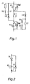
- the invention relates to a controlled diode recovery circuit (C.D.R. circuit) which is used with two semiconductor switches having anti-parallel diodes (either intrinsic to the switching device, or electrically connected to the switch), the circuit including a saturable inductor in series with the switching semiconductors.
- C.D.R. circuit controlled diode recovery circuit
- This circuit controls the reverse recovery current of diodes or of semiconductor switch body diodes. When a diode is reverse biased after carrying forward current, it takes some time to recover its blocking ability, while carriers recombine. This circuit will control the reverse current flowing during this time so that the recovering diode and the rest of the circuit are protected from large stresses which would otherwise be caused by huge reverse recovery current flowing.
- a method commonly used to control diode recovery current is to control (lower) the speed of the associated switching device. This method gives high losses in the switching device due to it carrying diode recovery current and output current (usually to an inductor) while in the linear region. The switching device will be in the linear region while the diode is recovering.
- a second method is to use a saturable (square loop) inductor in series with the diode.
- This inductor blocks the reverse current flow, without controlling its rate of increase, and greatly increases the recovery time of the diode.
- This method also has the problem of blocking forward current flow in the time it takes the inductor to saturate for current flow in that direction.
- a larger V.t (volt-time) rating of saturable inductor will be required than with the C.D.R. circuit according to the present invention, as this prior known circuit does not provide a controlled rate of reverse current flow (needed to recover the diode quickly).
- the a.c. chopper method varies the r.m.s. voltage while maintaining the input waveform frequency and shape.
- the a.c. chopper solves the problem with phase cutting controllers of line frequency harmonics and rise times, at the expense of higher cost and reduced efficiency.
- the novelties presented here help reduce the cost and increase efficiency of the a.c. chopper, though are not limited in use to this type of circuit.
- the C.D.R. circuit according to the present invention is designed to allow a controlled rate of increase in reverse recovery current so that the diode recovers quickly.
- the optimum rate of increase in reverse current for the application can be chosen. This also means the peak reverse current is also limited due to the rate of increase in reverse current and the speed of the diode.
- the C.D.R. circuit presents little impedance to current flow. This is because the circuit automatically provides a V.t across the saturable inductor, for forward conduction, after recovery of the diode to be recovered.
- the novel controlled diode recovery circuit according to the present invention when applied in the a.c. chopper, further reduces switching losses and device stresses, making the overall power conversion more efficient and reliable. This allows higher switching frequencies, smaller and lower rated components to be used, and higher efficiency, with significant cost savings.
- a further advantage of the C.D.R. circuit is that it allows the body diode of high speed switching semiconductors to be used at high switching frequencies, while giving low losses and low device stresses.
- the C.D.R. circuit presented here is a novel way to control the slope of the reverse recovery current of a diode, without having to control the turn on speed of the associated power switch, and also presenting minimum impedance or delay when the diode is required to conduct in the forward direction.
- a preferred embodiment of the invention is characterized in that in parallel with the second inductor, there is a series connection of a third diode and an impedance, the third diode and the main diode having the same forward direction.
- energy recovery is possible by making use of the energy transferred from the second inductor L2 to the impedance Z1 after recovery (see figure 1). Alternatively, this energy may be dissipated in Z1.
- the C.D.R. circuit may be used with two switches, connected in anti-series, allowing use with an a.c. supply (such as Fig. 1).
- the controlled diode recovery (C.D.R.) circuit is shown in figure 1 This circuit allows the corresponding power switch (such as switches M1-M2 in Fig. 1) to be turned on rapidly, without regard for the main diode (Dm1 or Dm2) recovery current slope or magnitude.
- the circuit connected to M1, M2, Dm1, Dm2, has the function of controlling the reverse recovery current of Dm1 and Dm2, while giving low power loss, and unhindered forward conduction of Dm1 and Dm2.
- L1 is a saturable inductor.
- the circuit of figure 1 is symmetrical. Operation will be described for forward current flow through Dm1. However, the description applies symmetrically to the case when forward flow is instead through Dm2. References to D2, D3, L2 or Z1 in the following, apply to the recovery circuit for Dm1, which is shown on the right of figure 1, connected across L1 and M2.
- L1 When Dm1 is next required to conduct, L1 will rapidly saturate (if not already saturated) during the fall time of the top rail voltage. D3 recovers during the time that Dm1 is carrying forward current flow.
- the C.D.R. circuit adds no significant conduction losses, and reduces switching losses due to the controlled reverse recovery current of the main diode.
- the circuit is symmetrical, so operation is identical when the voltage polarity across the rails is reversed, and the current flow is in the opposite direction (Dm2 carrying forward current), the symmetrically placed components being used instead of those described above.
- the saturable inductor, L1 has some finite inductance even when saturated. This means some energy is stored when current is flowing, causing a voltage spike across the switch being turned off. Provided the saturated inductance is small enough, the energy stored here will (usefully) charge the output capacitance of the switch being turned off.
- L1 Due to an imperfect hysteresis loop, L1 will allow some reverse current flow through Dm1, though this will be limited. This current adds to the controlled current slope, and will increase recovery speed but gives larger peak recovery current.
- circuit configurations which are covered by the same inventive concept. Such configurations are:
Landscapes
- Engineering & Computer Science (AREA)
- Power Engineering (AREA)
- Electronic Switches (AREA)
Applications Claiming Priority (3)
| Application Number | Priority Date | Filing Date | Title |
|---|---|---|---|
| FI980259A FI113915B (fi) | 1997-09-25 | 1998-02-05 | Piiri runkodiodin hallittua elpymistä varten |
| FI980259 | 1998-02-05 | ||
| EP98202840A EP0905873B1 (de) | 1997-09-25 | 1998-08-25 | Gesteuerte Dioden- oder Körperdiodenrückgewinnungsschaltung |
Related Parent Applications (1)
| Application Number | Title | Priority Date | Filing Date |
|---|---|---|---|
| EP98202840A Division EP0905873B1 (de) | 1997-09-25 | 1998-08-25 | Gesteuerte Dioden- oder Körperdiodenrückgewinnungsschaltung |
Publications (2)
| Publication Number | Publication Date |
|---|---|
| EP1237270A2 true EP1237270A2 (de) | 2002-09-04 |
| EP1237270A3 EP1237270A3 (de) | 2004-01-07 |
Family
ID=26150643
Family Applications (1)
| Application Number | Title | Priority Date | Filing Date |
|---|---|---|---|
| EP02010727A Withdrawn EP1237270A3 (de) | 1998-02-05 | 1998-08-25 | Gesteuerte Diodenrückgewinnungsschaltung |
Country Status (1)
| Country | Link |
|---|---|
| EP (1) | EP1237270A3 (de) |
Family Cites Families (4)
| Publication number | Priority date | Publication date | Assignee | Title |
|---|---|---|---|---|
| US3955131A (en) * | 1975-09-08 | 1976-05-04 | General Electric Company | Circuit for controlling the reverse current in a controlled rectifier |
| GB8816774D0 (en) * | 1988-07-14 | 1988-08-17 | Bsr Int Plc | Power supplies |
| US5107151A (en) * | 1989-08-22 | 1992-04-21 | Unique Mobility, Inc. | Switching circuit employing electronic devices in series with an inductor to avoid commutation breakdown and extending the current range of switching circuits by using igbt devices in place of mosfets |
| US5202820A (en) * | 1991-12-16 | 1993-04-13 | Ford Motor Company | Saturable inductor protection circuit for inductive load driver |
-
1998
- 1998-08-25 EP EP02010727A patent/EP1237270A3/de not_active Withdrawn
Also Published As
| Publication number | Publication date |
|---|---|
| EP1237270A3 (de) | 2004-01-07 |
Similar Documents
| Publication | Publication Date | Title |
|---|---|---|
| CA2271792C (en) | Voltage clamp snubbers for three level converter | |
| US6995992B2 (en) | Dual bridge matrix converter | |
| RU2674989C2 (ru) | Подмодуль, защитный блок, преобразователь и способ управления преобразователем | |
| EP0868014B1 (de) | Hochspannungsumrichter | |
| Bernet et al. | A matrix converter using reverse blocking NPT-IGBTs and optimized pulse patterns | |
| US20040037101A1 (en) | Cutting electric power converter | |
| JPH01274666A (ja) | Ac―dcコンバータ装置 | |
| Baharom et al. | A new single-phase controlled rectifier using single-phase matrix converter | |
| US4319318A (en) | Voltage reapplication rate control for commutation of thyristors | |
| US5625549A (en) | Boost-buck rectifier bridge circuit topology with diode decoupled boost stage | |
| US6137703A (en) | Clamped bidirectional power switches | |
| JP2020014045A (ja) | 双方向スイッチ回路 | |
| US4405977A (en) | Commutation circuits for thyristor inverters | |
| US20030160286A1 (en) | Protective circuit for a network-controlled thyristor bridge | |
| EP1237270A2 (de) | Gesteuerte Diodenrückgewinnungsschaltung | |
| Kerris et al. | Implementation of a matrix converter using p-channel MOS-controlled thyristors | |
| EP0905873B1 (de) | Gesteuerte Dioden- oder Körperdiodenrückgewinnungsschaltung | |
| JPH0720340B2 (ja) | インバータ | |
| CN1143279A (zh) | 换流器电路装置 | |
| CA1267702A (en) | Thyristor commutation circuit | |
| Deacon et al. | An evaluation of resonant snubbers applied to GTO converters | |
| Hanafi et al. | Improved switching strategy of single-phase matrix converter as a direct AC-AC converter | |
| EP0055684B1 (de) | Wechselrichter mit zugehörigem Kommutierungskreis | |
| CN1091972C (zh) | 一种软开关脉宽调制电路 | |
| EP0469003A1 (de) | Schaltungen mit schaltschutz und deren teile |
Legal Events
| Date | Code | Title | Description |
|---|---|---|---|
| PUAI | Public reference made under article 153(3) epc to a published international application that has entered the european phase |
Free format text: ORIGINAL CODE: 0009012 |
|
| AC | Divisional application: reference to earlier application |
Ref document number: 905873 Country of ref document: EP |
|
| AK | Designated contracting states |
Kind code of ref document: A2 Designated state(s): DE FR GB IT NL |
|
| AX | Request for extension of the european patent |
Free format text: AL;LT;LV;MK;RO;SI |
|
| PUAL | Search report despatched |
Free format text: ORIGINAL CODE: 0009013 |
|
| AK | Designated contracting states |
Kind code of ref document: A3 Designated state(s): DE FR GB IT NL |
|
| AX | Request for extension of the european patent |
Extension state: AL LT LV MK RO SI |
|
| 17P | Request for examination filed |
Effective date: 20040707 |
|
| AKX | Designation fees paid |
Designated state(s): DE FR GB IT NL |
|
| GRAP | Despatch of communication of intention to grant a patent |
Free format text: ORIGINAL CODE: EPIDOSNIGR1 |
|
| STAA | Information on the status of an ep patent application or granted ep patent |
Free format text: STATUS: THE APPLICATION IS DEEMED TO BE WITHDRAWN |
|
| 18D | Application deemed to be withdrawn |
Effective date: 20050413 |