EP1231636A2 - Semiconductor device, production method therefor, and electrophotographic apparatus - Google Patents
Semiconductor device, production method therefor, and electrophotographic apparatus Download PDFInfo
- Publication number
- EP1231636A2 EP1231636A2 EP02002265A EP02002265A EP1231636A2 EP 1231636 A2 EP1231636 A2 EP 1231636A2 EP 02002265 A EP02002265 A EP 02002265A EP 02002265 A EP02002265 A EP 02002265A EP 1231636 A2 EP1231636 A2 EP 1231636A2
- Authority
- EP
- European Patent Office
- Prior art keywords
- chip
- coil
- semiconductor device
- pattern
- coil pattern
- Prior art date
- Legal status (The legal status is an assumption and is not a legal conclusion. Google has not performed a legal analysis and makes no representation as to the accuracy of the status listed.)
- Withdrawn
Links
Images





Classifications
-
- G—PHYSICS
- G06—COMPUTING OR CALCULATING; COUNTING
- G06K—GRAPHICAL DATA READING; PRESENTATION OF DATA; RECORD CARRIERS; HANDLING RECORD CARRIERS
- G06K19/00—Record carriers for use with machines and with at least a part designed to carry digital markings
- G06K19/06—Record carriers for use with machines and with at least a part designed to carry digital markings characterised by the kind of the digital marking, e.g. shape, nature, code
- G06K19/067—Record carriers with conductive marks, printed circuits or semiconductor circuit elements, e.g. credit or identity cards also with resonating or responding marks without active components
- G06K19/07—Record carriers with conductive marks, printed circuits or semiconductor circuit elements, e.g. credit or identity cards also with resonating or responding marks without active components with integrated circuit chips
- G06K19/077—Constructional details, e.g. mounting of circuits in the carrier
-
- G—PHYSICS
- G06—COMPUTING OR CALCULATING; COUNTING
- G06K—GRAPHICAL DATA READING; PRESENTATION OF DATA; RECORD CARRIERS; HANDLING RECORD CARRIERS
- G06K19/00—Record carriers for use with machines and with at least a part designed to carry digital markings
- G06K19/06—Record carriers for use with machines and with at least a part designed to carry digital markings characterised by the kind of the digital marking, e.g. shape, nature, code
- G06K19/067—Record carriers with conductive marks, printed circuits or semiconductor circuit elements, e.g. credit or identity cards also with resonating or responding marks without active components
- G06K19/07—Record carriers with conductive marks, printed circuits or semiconductor circuit elements, e.g. credit or identity cards also with resonating or responding marks without active components with integrated circuit chips
- G06K19/077—Constructional details, e.g. mounting of circuits in the carrier
- G06K19/07749—Constructional details, e.g. mounting of circuits in the carrier the record carrier being capable of non-contact communication, e.g. constructional details of the antenna of a non-contact smart card
- G06K19/0775—Constructional details, e.g. mounting of circuits in the carrier the record carrier being capable of non-contact communication, e.g. constructional details of the antenna of a non-contact smart card arrangements for connecting the integrated circuit to the antenna
-
- G—PHYSICS
- G06—COMPUTING OR CALCULATING; COUNTING
- G06K—GRAPHICAL DATA READING; PRESENTATION OF DATA; RECORD CARRIERS; HANDLING RECORD CARRIERS
- G06K19/00—Record carriers for use with machines and with at least a part designed to carry digital markings
- G06K19/06—Record carriers for use with machines and with at least a part designed to carry digital markings characterised by the kind of the digital marking, e.g. shape, nature, code
- G06K19/067—Record carriers with conductive marks, printed circuits or semiconductor circuit elements, e.g. credit or identity cards also with resonating or responding marks without active components
- G06K19/07—Record carriers with conductive marks, printed circuits or semiconductor circuit elements, e.g. credit or identity cards also with resonating or responding marks without active components with integrated circuit chips
- G06K19/077—Constructional details, e.g. mounting of circuits in the carrier
- G06K19/07749—Constructional details, e.g. mounting of circuits in the carrier the record carrier being capable of non-contact communication, e.g. constructional details of the antenna of a non-contact smart card
-
- H—ELECTRICITY
- H10—SEMICONDUCTOR DEVICES; ELECTRIC SOLID-STATE DEVICES NOT OTHERWISE PROVIDED FOR
- H10W—GENERIC PACKAGES, INTERCONNECTIONS, CONNECTORS OR OTHER CONSTRUCTIONAL DETAILS OF DEVICES COVERED BY CLASS H10
- H10W44/00—Electrical arrangements for controlling or matching impedance
- H10W44/501—Inductive arrangements
-
- H—ELECTRICITY
- H10—SEMICONDUCTOR DEVICES; ELECTRIC SOLID-STATE DEVICES NOT OTHERWISE PROVIDED FOR
- H10W—GENERIC PACKAGES, INTERCONNECTIONS, CONNECTORS OR OTHER CONSTRUCTIONAL DETAILS OF DEVICES COVERED BY CLASS H10
- H10W70/00—Package substrates; Interposers; Redistribution layers [RDL]
- H10W70/01—Manufacture or treatment
- H10W70/05—Manufacture or treatment of insulating or insulated package substrates, or of interposers, or of redistribution layers
-
- H—ELECTRICITY
- H10—SEMICONDUCTOR DEVICES; ELECTRIC SOLID-STATE DEVICES NOT OTHERWISE PROVIDED FOR
- H10W—GENERIC PACKAGES, INTERCONNECTIONS, CONNECTORS OR OTHER CONSTRUCTIONAL DETAILS OF DEVICES COVERED BY CLASS H10
- H10W70/00—Package substrates; Interposers; Redistribution layers [RDL]
- H10W70/60—Insulating or insulated package substrates; Interposers; Redistribution layers
- H10W70/699—Insulating or insulated package substrates; Interposers; Redistribution layers for flat cards, e.g. credit cards
-
- H—ELECTRICITY
- H10—SEMICONDUCTOR DEVICES; ELECTRIC SOLID-STATE DEVICES NOT OTHERWISE PROVIDED FOR
- H10W—GENERIC PACKAGES, INTERCONNECTIONS, CONNECTORS OR OTHER CONSTRUCTIONAL DETAILS OF DEVICES COVERED BY CLASS H10
- H10W72/00—Interconnections or connectors in packages
- H10W72/01—Manufacture or treatment
- H10W72/0198—Manufacture or treatment batch processes
-
- H—ELECTRICITY
- H10—SEMICONDUCTOR DEVICES; ELECTRIC SOLID-STATE DEVICES NOT OTHERWISE PROVIDED FOR
- H10W—GENERIC PACKAGES, INTERCONNECTIONS, CONNECTORS OR OTHER CONSTRUCTIONAL DETAILS OF DEVICES COVERED BY CLASS H10
- H10W72/00—Interconnections or connectors in packages
- H10W72/50—Bond wires
- H10W72/551—Materials of bond wires
- H10W72/552—Materials of bond wires comprising metals or metalloids, e.g. silver
- H10W72/5522—Materials of bond wires comprising metals or metalloids, e.g. silver comprising gold [Au]
-
- H—ELECTRICITY
- H10—SEMICONDUCTOR DEVICES; ELECTRIC SOLID-STATE DEVICES NOT OTHERWISE PROVIDED FOR
- H10W—GENERIC PACKAGES, INTERCONNECTIONS, CONNECTORS OR OTHER CONSTRUCTIONAL DETAILS OF DEVICES COVERED BY CLASS H10
- H10W72/00—Interconnections or connectors in packages
- H10W72/50—Bond wires
- H10W72/551—Materials of bond wires
- H10W72/552—Materials of bond wires comprising metals or metalloids, e.g. silver
- H10W72/5524—Materials of bond wires comprising metals or metalloids, e.g. silver comprising aluminium [Al]
-
- H—ELECTRICITY
- H10—SEMICONDUCTOR DEVICES; ELECTRIC SOLID-STATE DEVICES NOT OTHERWISE PROVIDED FOR
- H10W—GENERIC PACKAGES, INTERCONNECTIONS, CONNECTORS OR OTHER CONSTRUCTIONAL DETAILS OF DEVICES COVERED BY CLASS H10
- H10W74/00—Encapsulations, e.g. protective coatings
-
- H—ELECTRICITY
- H10—SEMICONDUCTOR DEVICES; ELECTRIC SOLID-STATE DEVICES NOT OTHERWISE PROVIDED FOR
- H10W—GENERIC PACKAGES, INTERCONNECTIONS, CONNECTORS OR OTHER CONSTRUCTIONAL DETAILS OF DEVICES COVERED BY CLASS H10
- H10W90/00—Package configurations
- H10W90/701—Package configurations characterised by the relative positions of pads or connectors relative to package parts
- H10W90/751—Package configurations characterised by the relative positions of pads or connectors relative to package parts of bond wires
- H10W90/756—Package configurations characterised by the relative positions of pads or connectors relative to package parts of bond wires between a chip and a stacked lead frame, conducting package substrate or heat sink
Definitions
- the present invention relates to a semiconductor apparatus, which has at least an IC chip, and a coil connected to the IC chip and performs information transmission by using an induction field as a transmission medium, a production method therefor, and an electrophotographic apparatus having the semiconductor device mounted thereon.
- non-contacting type semiconductor devices such as non-contact type IC tags and non-contact type IC cards are spreading, the non-contacting type semiconductor devices each incorporating a coil for an antenna, which transmits and receives data via an electromagnetic wave, and an IC chip in which a semiconductor element performing the recording and processing of data is mounted.
- this non-contact type semiconductor device comprises a coil for an antenna for transmitting and receiving a data signal and electric power between the coil and a reader-writer which performs reading and writing of data, electronic parts such as an IC chip for processing the above-described signal, and a substrate which connects and supports the coil for an antenna, and the electronic parts.
- Japanese Patent Application Laid-Open No. 11-144018 discloses a non-contact type IC card formed by forming a hot melt layer on a substrate, forming a coil for an antenna by making a wire such as a copper wire, supplied from a pulley, wound around the hot melt layer and embedded, connecting the coil for an antenna with an IC chip arranged near the center of the hot melt layer, and further covering them with an over film.
- Japanese Patent Application Laid-Open No. 10-337982 discloses a non-contact type IC card formed by forming on a substrate a coil-shaped copper foil etching pattern which serves as an antenna by etching, and simultaneously forming a die pad for mounting an IC chip, and then connecting the IC chip, which is mounted on the die pad, to the copper foil etching pattern by wire bonding, and further bonding and fixing the substrate with an electroconductive adhesive.
- Japanese Patent Application Laid-Open No. 11-250214 discloses a non-contact type IC card formed by forming a coil for an antenna by printing conductive paste in a coiled shape on a substrate, connecting an IC chip to the coil for an antenna by jumpers after mounting the IC chip on the substrate, fixing the IC chip by hardening the conductive paste, and performing hot stamping after laminating a film material over the substrate.
- a substrate is indispensable in order to arrange a coil for an antenna in formation of a semiconductor device such as an IC card. Therefore, since material cost relating to the substrate is irreducible, this becomes one of factors that disturb the cost reduction of an IC card. In addition, this is also a factor that disturbs weight reduction that is an important specification required of an IC card.
- the present invention has been made in view of the above-described problems, and aims to provide a semiconductor device which has reduced a production cost including a material cost by not only reducing the material cost of an IC card, but also lightening the IC card by omitting a substrate, and simplifying production process therefor, and a production method therefor.
- a semiconductor device is a semiconductor device comprising an IC chip and a coil connected to the IC chip, in which information transmission is performed by using as a transmission medium an induction field generated from the coil, and is characterized in that the coil and connecting terminals connected to the coil and electrically connected to the IC chip are formed of the same metal plate which is patterned.
- a semiconductor device is characterized in that the above-described IC chip, coil, and connecting terminals are integrated by being encapsulated with a resin.
- a semiconductor device is a semiconductor device comprising an IC chip and a coil connected to the IC chip, in which information transmission is performed by using as a transmission medium an induction field generated from the coil, and is characterized in that an IC chip supporting section where the IC chip is mounted, the coil, and the connecting terminals connected to the coil and electrically connected to the IC chip are formed of the same metal plate which is patterned.
- a semiconductor device is characterized in that the above-described IC chip, IC chip supporting section, coil, and connecting terminals are integrated by being encapsulated with a resin.
- a semiconductor device is characterized in that at least one side of the above-described coil is exposed from a surface of the above-described resin.
- a semiconductor device is characterized in that the above-described IC chip and the above-described connecting terminals are connected with jumpers, and the jumpers are also encapsulated with the above-described resin.
- a semiconductor device is characterized in that the above-described IC chip and the above-described connecting terminals are connected in flip chip connection.
- a semiconductor device is characterized in that a part of one side of the above-described coil is bonded and fixed with a tape.
- a method of producing a semiconductor device is characterized by comprising: a step of forming a metal frame having at least a coil pattern for forming a coil for generating an induction field, and a connecting terminal pattern for electrical connection to the above-described IC chip by connection to the above-described coil pattern, from the same metal plate; a step of electrically connecting the connecting terminal pattern and the IC chip; and a step of encapsulating the IC chip and the metal frame with a resin.
- a method of producing a semiconductor device is characterized by comprising: a step of forming a metal frame having at least an IC chip supporting section pattern for supporting an IC chip, a coil pattern for forming a coil for generating an induction field, and a connecting terminal pattern for electrical connection to the above-described IC chip by connection to the above-described coil pattern, from the same metal plate; a step of mounting the IC chip on the IC chip supporting section and electrically connecting the connecting terminal pattern and the mounted IC chip; and a step of encapsulating the IC chip and the metal frame with a resin.
- a method of producing a semiconductor device according to the present invention is characterized in that the above-described metal frame is patterned by stamping or etching.
- a method of producing a semiconductor device according to the present invention is characterized by further comprising a step of sticking a tape for fixing a coil pattern on a part of one side of the above-described coil pattern.
- a method of producing a semiconductor device according to the present invention is characterized in that tying sections tying respective portions of the above-described coil pattern are formed in the above-described metal frame, and that the tying sections are cut after sticking the above-described tape.
- a method of producing a semiconductor device according to the present invention is characterized in that the above-described IC chip and the above-described connecting terminal pattern are electrically connected by wire bonding, and that jumpers formed by bonding are also encapsulated with the above-described resin.
- a method of producing a semiconductor device according to the present invention is characterized in that the above-described IC chip and the above-described connecting terminal pattern are electrically connected in flip chip connection.
- an electrophotographic apparatus is characterized by including a process cartridge where the above-described semiconductor device is stuck.
- This embodiment relates to a non-contact type IC tag having an IC chip and a coil connected to the IC chip, wherein the IC chip is mounted on an IC chip supporting section, wherein the IC chip and the coil are connected by wire bonding that uses a gold or aluminum wire, and wherein resin encapsulation is performed.
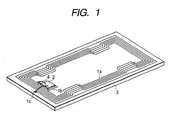
- FIG. 1 is a transparent perspective view showing the configuration of a non-contact type IC tag according to this embodiment
- FIG. 2 is a schematic sectional view thereof.
- reference character 1a denotes a coil pattern section formed by winding a strip pattern multiple times in the shape of a coil.
- the coil pattern section 1a becomes a coil for an antenna that is used in the IC tag of the present invention performing information transmission by using external parts and an electromagnetic wave as a transmission medium.
- An IC chip 2 performs the recording and processing of data transmitted and received by the coil pattern section 1a.
- the IC chip 2 is mounted on an IC chip supporting section 1b.
- Connecting terminal 1c is provided at the end of the coil pattern section 1a, and is connected to the IC chip 2.
- FIG. 4 is a plan showing only the coil pattern section la, IC chip supporting section 1b, and mounting pad 1c that are produced by patterning.
- the IC chip 2 is mounted (die-bonded) on the IC chip supporting section 1b, and connecting terminals of the IC chip 2 (not shown) are electrically connected to the connecting terminals 1c provided in both ends of the coil pattern section 1a with gold or aluminum wires 4 by wire bonding.
- An encapsulating resin material 3 encapsulates the coil pattern section 1a, IC chip supporting section 1b, connecting terminals 1c, IC chip 2, and wires 4.
- the encapsulating resin material 3 fixes the coil pattern section 1a, IC chip supporting section 1b, connecting terminals 1c, IC chip 2, and wires 4 to integrate them into a plate-like IC tag.
- the encapsulating resin material 3 encapsulates the IC chip 2 and wires 4 fully, and encapsulates the coil pattern section 1a, IC chip supporting section 1b, and connecting terminals 1c so that each one side of them may be exposed from the encapsulating resin material 3. It becomes possible to enhance the reliability of transmission and reception of an electromagnetic wave used as a transmission medium by exposing each one side.
- the encapsulating resin material 3 encapsulates the coil pattern section 1a, IC chip supporting section 1b, connecting terminals 1c, IC chip 2, and wires 4
- the encapsulating resin material 3 may also fully encapsulate the coil pattern section 1a, IC chip supporting section 1b, and connecting terminals 1c in addition to the IC chip 2 and wires 4. It is possible to more securely fix the coil pattern section 1a, IC chip supporting section 1b, and connecting terminals 1c by fully encapsulating them.
- environment resistance at the time of using it as an IC tag is enhanced and it can normally operate while being hardly influenced by a change of temperature, humidity, or the like, whereby the reliability of operation as the IC tag is enhanced.
- Whether one side of each of the coil pattern section 1a, IC chip supporting section 1b, and connecting terminals 1c is exposed or whole surfaces thereof is encapsulated can be just selected optionally according to a purpose of use, an operating environment, etc.
- FIGS. 5A to 5D and FIG. 10 the steps of a method of producing the above-described non-contact type IC tag will be described referring to FIGS. 5A to 5D and FIG. 10.
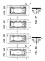
- FIGS. 5A to 5D and FIGS. 6A to 6F are sectional views and plan views for explaining the production steps of a frame for the IC tag which consists of the coil pattern section 1a, IC chip supporting section 1b, connecting terminals 1c, and an outer frame section 1d which supports them.
- a photosensitive material 11 consisting of a liquid resist or a dry film resist is applied on an iron-nickel plate 10 (a single plate or a hoop) having a size of 43 mm in width, 200 mm in length and 0.4 mm in thickness.
- a pattern of the coil pattern 1a, and the IC chip supporting section 1b, a pattern of the connecting terminals 1c, and a pattern of the outer frame section 1d are printed on the metal plate 10, on which the photosensitive material 11 is applied, by using a mask not shown, and are developed by using a chemical developer consisting of sodium carbonate, meta-silicic acid, a solvent, etc.
- etching is performed up to the back face of the iron-nickel plate 10 by using etchant such as copper chloride and ferric chloride.
- the photosensitive material 11 used as the resist of etching is peeled by using alkali peel liquid such as sodium hydroxide, caustic potash, and a solvent.
- alkali peel liquid such as sodium hydroxide, caustic potash, and a solvent.
- the step of patterning the frame pattern it is also possible to perform the patterning by stamping instead of the above-described etching.
- the patterning is performed by stamping an iron-nickel plate with a stamping die having the frame pattern consisting of the coil pattern section 1a, IC chip supporting section 1b, connecting terminals 1c, and their outer frame section 1d.
- FIG. 6A shows an iron-nickel plate 20 patterned according to FIGS. 5A to 5D.
- the patterned iron-nickel plate 20 shown in FIG. 6A connects respective portions of the coil pattern section 1a with a tying sections 1e shown in FIG. 6E so that the coil pattern section 1a should be deformed in the shape of a spring in the direction perpendicular to the patterned iron-nickel plate 20.
- the tying sections partially connect the outermost periphery of the coil pattern section 1a to the outer frame section 1d.
- the tying sections 1e also connects to the IC chip supporting section 1b to prevent its deformation.
- the IC chip supporting section 1b and connecting terminals 1c are plated with silver or gold. Furthermore, as shown in FIG. 6C, sheets of tape 6 are partially stuck on one side of the coil pattern section 1a in the patterned iron-nickel plate 20.
- the sheets of tape 6 each have the size of not disturbing a function of the coil pattern section 1a as an antenna, and fix the coil pattern section 1a.
- the sheets of tape 6 further strengthen the prevention of deformation of the coil pattern section 1a by the tying sections 1e, and the patterned iron-nickel plate 20 never deforms even if being transferred to the next step.
- tying portions, tying respective portions of the coil pattern section 1a, and tying portions with the IC chip supporting section 1b in the tying sections 1e are cut with a cutter or a press, which is not shown, as shown in FIG. 6F.
- tying portions connecting the outermost periphery of the coil pattern section 1a in the tying sections 1e to the outer frame section id are not cut. Even if the tying portions connecting respective portions of the coil pattern section 1a in the tying sections 1e, and the tying portions with the IC chip supporting section 1b are cut, the coil pattern section 1a is never deformed since being fixed by the sheets of tape 6.
- the tying portions connecting respective portions of the coil pattern section 1a in the tying sections 1e, and the tying portions with the IC chip supporting section 1b are not always indispensable. If the coil pattern section 1a and IC chip supporting section 1b have high rigidity, they have sufficient rigidity without the tying sections 1e, and are not deformed, whereby the above-described typing sections are not necessary. In this case, the taping step shown in FIG. 6C and the cutting step of the tying sections 1e that is shown in FIG. 6D are unnecessary.
- a frame 25 for an IC tag is produced using the steps shown in FIGS. 5A to 5D and 6A to 6F.
- FIG. 7 the production process of an IC tag using the frame 25 for an IC tag produced through the steps shown in FIGS. 5A to 5D and FIGS. 6A to 6F will be described.
- a plurality of IC chips is formed by oxidizing a 5 to 8 inch Si wafer and performing steps such as photo-etching.
- the thickness of the plurality of IC chips is adjusted by performing wafer back grinding if needed. Wafer back grinding makes it possible to thin the IC tag, to lighten the IC tag, and to reduce the cost of the encapsulating resin material 3.
- the IC chips 2 are produced by dividing (wafer-dicing) the plurality of IC chips formed on the Si wafer at STEP 1.
- the IC chip 2 produced at STEP 2 is bonded and fixed (die-bonded) on the IC chip supporting section 1b of the frame 25 for an IC tag produced at the step shown in FIGS. 6A to 6F.
- the IC chip 2 and connecting terminals 1c of the frame 25 for an IC tag are electrically connected with gold or aluminum wires 4 by wire bonding.
- reference numeral 30 denotes a fixed die and reference numeral 31 denotes a movable die.
- the frame 25 for an IC tag is held on the fixed die 30.
- the outer frame section 1d of the frame 25 for an IC tag is arranged so that the outer frame section 1d may be located in the outside of a mold cavity 32, into which the encapsulating resin material 3 is injected, and that the outer frame section 1d is not encapsulated with the encapsulating resin material 3.
- the fixed die 30 and movable die 31 are opened after injecting the encapsulating resin material 3 into the mold cavity 32 and curing the encapsulating resin material 3, and the frame 25 for an IC tag covered with the encapsulating resin material 3 is taken out.
- the IC tag is completed by cutting the tying portions 1e, which tie the outermost periphery of the coil pattern section 1a with the outer frame section 1d and are not cut at the step shown in FIG. 6D, and separating the outer frame section 1d from the IC tag.
- the IC tag is produced by passing through the above steps.
- a plurality of IC tags according to this embodiment may be produced simultaneously from the same metal frame.
- the IC tags can be separated from the outer frame sections 1d of the frame 20 for IC tags simultaneously, or can be cut in order.
- an iron-nickel plate is used as a metal frame in this embodiment, another material, for example, a copper plate can be also used.
- This embodiment relates to a non-contact type IC tag that has an IC chip and a coil connected to the IC chip, and is encapsulated with a resin after the electrical connection of the IC chip and coil in flip chip connection.
- FIG. 11 is a plan showing the configuration of a non-contact type IC tag according to this embodiment
- FIG. 12 is a sectional view thereof.
- the same reference characters are assigned to the same members as those in Embodiment 1.
- reference character 1a denotes a coil pattern section formed by winding a strip multiple times in the shape of a coil.
- the coil pattern section 1a becomes a coil for an antenna that is used in this IC tag performing information transmission by using external parts and an electromagnetic wave as a transmission medium.
- An IC chip 2 performs the recording and processing of data transmitted and received by the coil pattern section 1a.
- Connecting terminal 1c is provided at the end of the coil pattern section 1a, and is connected to the IC chip 2.
- the coil pattern section 1a and connecting terminals 1c are made by performing patterning by etching or pressing (stamping) the same iron-nickel plate.
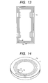
- FIG. 13 is a plan showing only the coil pattern section 1a and connecting terminals 1c that are produced by patterning.
- the IC chip 2 is electrically connected with connecting terminals 1c in flip chip connection through bumps 5 such as Au bumps or solder bumps.
- An encapsulating resin material 3 encapsulates the coil pattern section 1a, IC chip supporting section 1b, connecting terminals 1c, IC chip 2, and wires 4.
- a connection material other than a metal bump, such as an anisotropy electroconductive film may be also used as each of the bumps 5.
- coil pattern section 1a, connecting terminal 1c, and IC chip 2 are encapsulated so that each one side of an iron-nickel frame may be exposed from an encapsulating resin material 3 as shown in FIG. 12, similarly to Embodiment 1, the coil pattern section 1a, connecting terminal 1c, and IC chip 2 may be thoroughly encapsulated with the resin material.
- Embodiment 1 For an IC tag according to this embodiment, it is possible to use a production method that is the almost same as that in Embodiment 1 described by using FIGS. 5A through 10.
- the difference from Embodiment 1 is the point of electrically connecting the IC chip 2 to the connecting terminal 1c in flip chip connection by using the bumps 5 instead of the die bonding step shown in STEP 3 and the wire bonding step shown in STEP 4 in FIG. 7.
- an iron-nickel plate is used as a metal frame in this embodiment, another material, for example, a copper plate can be also used.
- IC tag with rectangular geometry is used and described as the examples as shown in FIGS. 1 and 11, geometry is not especially limited, and hence, for example, as shown in FIG. 14, round geometry can be used.
- a coil pattern section may be divided into two portions and arrange them, and to arrange an IC chip in a center section.
- a semiconductor device can use as a non-contacting type IC card, an IC tag, or the like where an IC chip including a microprocessor and semiconductor memory such as RAM and ROM, and a coil for functioning as an electric power supply and a communication antenna are mounted. Also, a battery for applying a voltage to the IC chip may be provided, if necessary.
- the IC tag performs information transmission via an induction field in a comparatively short distance, and hence, is used for an application requiring a medium smaller and lighter than an IC card.
- the non-contacting type IC card can be used for the payment of a ticket fare, bank dealings, identification, and record of information such as a clinical history.
- the non-contacting type IC tag can be used for the recording of process management information such as a lot number of a product, and the recording of operating conditions such as a usage count after product sale, and of use restriction information, etc.
- FIGS. 16 and 17 An example where the IC tag according to the present invention is applied to a process cartridge used for an image formation apparatus will be described with referring to FIGS. 16 and 17.
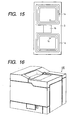
- FIG. 16 is a perspective view of an image formation apparatus 100 where a process cartridge is used.
- An electrophotography copying machine, an electrophotographic printer, etc. are included as examples of the image formation apparatus.
- FIG. 17 is a perspective view of a process cartridge 200 used for the image formation apparatus 100 shown in FIG. 16.
- the process cartridge is a cartridge that is made by integrating charging means, developing means or cleaning means, and an electrophotographic photosensitive member, and is detachable from a body of the image formation apparatus.
- the process cartridge is a cartridge that is made by integrating at least one of charging means, developing means, and cleaning means, and an electrophotographic photosensitive member, and is detachable from a body of the image formation apparatus.
- the process cartridge is a cartridge that is made by integrating at least one of developing means, and an electrophotographic photosensitive member, and is detachable from a body of the image formation apparatus.
- reference numeral 300 denotes the IC tag stuck on the process cartridge 200.
- the process cartridge 200 that contains toner is an interchangeable unit that needs to be exchanged at the time of exhaustion of the toner. Such an interchangeable unit is exchanged by performing residual quantity detection of toner etc. and reporting exchange time to a user.
- a user can exactly grasp a use state of the consumable as well as exchange time, and hence, for example, when the user is going to print many documents, it becomes information for determining whether the consumable is fully new.
- a use state can be exactly grasped.
- a transmitter-receiver that is not shown and is provided in the image formation apparatus 100 reads use restriction information such as time that corresponds to the amount of the toner and is stored beforehand in the IC tag 300.
- the above-described transmitter-receiver provided in the image formation apparatus 100 writes use information such as actually used time in the IC tag 300.
- a substrate used up to now by forming a semiconductor device such as an IC tag and an IC card by encapsulating an IC chip supporting section, a coil for an antenna and connecting terminals which are patterned and formed by stamping or etching of the same metal plate, as well as an IC chip mounted on the IC chip supporting section, with an encapsulating resin material.
- a semiconductor device such as an IC tag and an IC card
- a coil for an antenna and connecting terminals which are patterned and formed by stamping or etching of the same metal plate, as well as an IC chip mounted on the IC chip supporting section, with an encapsulating resin material.
- an IC chip supporting section by forming a semiconductor device such as an IC tag and an IC card by encapsulating a coil for an antenna and connecting terminals which are patterned and formed by stamping or etching of the same metal plate, as well as an IC chip mounted in flip chip connection, with an encapsulating resin material.
- a space where a coil is formed becomes large, it is possible to upgrade functions as an antenna.
- tying sections tying respective portions of the coil pattern section, tying the outermost periphery of the coil pattern section with the outer frame sections 1d, and tying the coil pattern section with the IC chip supporting section 1b are formed. This prevents that the coil pattern section deforms during production. In addition, on one side of the coil pattern section, pieces of tape are stuck partially.
- the deformation of the coil pattern section is further suppressed, and, even when the tying portions between portions of the coil pattern section and tying portions between the coil pattern section and the IC chip supporting section 1b are cut, the coil pattern section does not deform.
- a semiconductor device by mounting an IC chip, produced by using wafer back grinding, on the semiconductor device such as an IC tag or an IC card.
- a semiconductor device produced according to the present invention can be mounted in a process cartridge of an electrophotographic apparatus without considering a space.
- the semiconductor device of the present invention comprises an IC chip, and a coil connected to the IC chip, in which information is transmitted by using as a transmission medium an induction field generated from the coil, characterized in that the coil, and connecting terminals connected to the coil and electrically connected to the IC chip are formed of the same metal plate that is patterned.
Landscapes
- Engineering & Computer Science (AREA)
- Microelectronics & Electronic Packaging (AREA)
- Computer Hardware Design (AREA)
- Physics & Mathematics (AREA)
- General Physics & Mathematics (AREA)
- Theoretical Computer Science (AREA)
- Credit Cards Or The Like (AREA)
- Semiconductor Integrated Circuits (AREA)
Abstract
Description
Claims (18)
- A semiconductor device comprising an IC chip, and a coil connected to the IC chip, in which information is transmitted by using as a transmission medium an induction field generated from the coil,
characterized in that the coil, and connecting terminals connected to the coil and electrically connected to the IC chip are formed of the same metal plate that is patterned. - The semiconductor device according to claim 1, characterized in that the IC chip, the coil, and the connecting terminals are encapsulated with a resin to be integrated with one another.
- The semiconductor device comprising an IC chip, and a coil connected to the IC chip, in which information is transmitted by using as a transmission medium an induction field generated from the coil,
characterized in that an IC chip supporting section where the IC chip is mounted, the coil, and connecting terminals connected to the coil and electrically connected to the IC chip are formed of the same metal plate that is patterned. - The semiconductor device according to claim 3, characterized in that the IC chip, the IC chip supporting section, the coil, and the connecting terminals are encapsulated with a resin to be integrated with one another.
- The semiconductor device according to claims 2 or 4, characterized in that at least one side of the coil is exposed from a surface of the resin.
- The semiconductor device according to claims 2 or 4, characterized in that the IC chip and the connecting terminals are connected by wires, and the wires are encapsulated with the resin.
- The semiconductor device according to claims 2 or 4, characterized in that the IC chip and the connecting terminals are connected in flip chip connection.
- The semiconductor device according to claims 2 or 4, characterized in that a part of one side of the coil is bonded and fixed with a tape.
- A method of producing a semiconductor device that transmits information by using as a transmission medium an induction field generated from a coil electrically connected to an IC chip, characterized by comprising the steps of:forming a metal frame having at least a coil pattern for forming a coil for generating the induction field, and a connecting terminal pattern for connection to the coil pattern and electrical connection to the IC chip, from the same metal plate;mounting the IC chip on the metal frame;electrically connecting the connecting terminal pattern to the IC chip; andencapsulating the IC chip and the metal frame with a resin.
- A method of producing a semiconductor device that transmits information by using as a transmission medium an induction field generated from a coil electrically connected to an IC chip, characterized by comprising the steps of:forming a metal frame having at least an IC chip supporting section pattern for supporting the IC chip, a coil pattern for forming a coil for generating the induction field, and a connecting terminal pattern for connection to the coil pattern and electrical connection to the IC chip, from the same metal plate;mounting the IC chip on the IC chip supporting section and electrically connecting the connecting terminal pattern to the IC chip that is mounted; andencapsulating the IC chip and the metal frame with a resin.
- The method of producing a semiconductor device according to claims 9 or 10, characterized in that patterning of the metal plate is performed by stamping or etching.
- The method of producing a semiconductor device according to claims 9 or 10, characterized in that electrical connection of the connecting terminal pattern and the IC chip is performed by wire bonding, and that wires formed by the wire bonding are encapsulated with the resin.
- The method of producing a semiconductor device according to claim 9, characterized in that electrical connection of the connecting terminal pattern and the IC chip is performed in flip chip connection.
- The method of producing a semiconductor device according to claims 9 or 10, characterized by further comprising a step of sticking a tape for coil pattern fixation on a part of one side of the coil pattern after the connecting terminal pattern and the IC chip are electrically connected.
- A method of producing a semiconductor device that transmits information by using as a transmission medium an induction field generated from a coil electrically connected to an IC chip, characterized by comprising the steps of:preparing one sheet of metal plate;forming a metal frame having at least a coil pattern, a connecting terminal pattern formed at an end of the coil pattern, and a tying section tying respective portions of the coil pattern, by patterning the metal plate;mounting the IC chip on the metal frame;electrically connecting the connecting terminal pattern to the IC chip;sticking a tape for coil pattern fixation on a part of one side of the coil pattern;cutting the tying section; andencapsulating the IC chip and the metal frame with a resin to integrate them.
- A method of producing a semiconductor device that transmits information by using as a transmission medium an induction field generated from a coil electrically connected to an IC chip, characterized by comprising the steps of:preparing one sheet of metal plate;forming a metal frame having at least a coil pattern, a connecting terminal pattern formed at an end of the coil pattern, an outer frame section, and a tying section tying respective portions of the coil pattern and tying the coil pattern and the outer frame section, by patterning the metal plate;mounting the IC chip on the metal frame;electrically connecting the connecting terminal pattern to the IC chip;sticking a tape for coil pattern fixation on a part of one side of the coil pattern after the connecting terminal pattern and the IC chip are electrically connected;cutting the tying section tying respective portions of the coil pattern;encapsulating the IC chip and the metal frame with a resin to integrate them; andcutting the tying section tying the coil pattern and the outer frame section.
- The method of producing a semiconductor device according to claim 16, characterized in that a plurality of semiconductor devices is produced from the one sheet of the metal plate.
- An electrophotographic apparatus characterized by comprising:a process cartridge on which the semiconductor device according to any one of claims 1 to 4 is stuck and which is detachably mounted on the electrophotographic apparatus; anda transmission-reception unit for transmitting information to and receiving information from the semiconductor device.
Applications Claiming Priority (4)
| Application Number | Priority Date | Filing Date | Title |
|---|---|---|---|
| JP2001023871 | 2001-01-31 | ||
| JP2001023871 | 2001-01-31 | ||
| JP2002009926A JP2002319011A (en) | 2001-01-31 | 2002-01-18 | Semiconductor device, method of manufacturing semiconductor device, and electrophotographic apparatus |
| JP2002009926 | 2002-01-18 |
Publications (2)
| Publication Number | Publication Date |
|---|---|
| EP1231636A2 true EP1231636A2 (en) | 2002-08-14 |
| EP1231636A3 EP1231636A3 (en) | 2005-02-02 |
Family
ID=26608653
Family Applications (1)
| Application Number | Title | Priority Date | Filing Date |
|---|---|---|---|
| EP02002265A Withdrawn EP1231636A3 (en) | 2001-01-31 | 2002-01-30 | Semiconductor device, production method therefor, and electrophotographic apparatus |
Country Status (5)
| Country | Link |
|---|---|
| US (1) | US20020125546A1 (en) |
| EP (1) | EP1231636A3 (en) |
| JP (1) | JP2002319011A (en) |
| KR (1) | KR20020064197A (en) |
| CN (1) | CN1184685C (en) |
Families Citing this family (21)
| Publication number | Priority date | Publication date | Assignee | Title |
|---|---|---|---|---|
| JP2003100980A (en) * | 2001-09-27 | 2003-04-04 | Hamamatsu Photonics Kk | Semiconductor device and manufacturing method thereof |
| US6818985B1 (en) * | 2001-12-22 | 2004-11-16 | Skyworks Solutions, Inc. | Embedded antenna and semiconductor die on a substrate in a laminate package |
| JP2005517592A (en) * | 2002-02-19 | 2005-06-16 | コーニンクレッカ フィリップス エレクトロニクス エヌ ヴィ | Method for manufacturing a transponder |
| CA2518589C (en) * | 2003-03-12 | 2009-12-22 | Bundesdruckerei Gmbh | Method for the production of a book cover insert and book cover insert for a book binding |
| JP2006057762A (en) * | 2004-08-20 | 2006-03-02 | Ntn Corp | Auto-tensioner |
| US7380190B2 (en) * | 2004-12-15 | 2008-05-27 | Impinj, Inc. | RFID tag with bist circuits |
| US7312622B2 (en) * | 2004-12-15 | 2007-12-25 | Impinj, Inc. | Wafer level testing for RFID tags |
| US7307528B2 (en) * | 2004-12-15 | 2007-12-11 | Impinj, Inc. | RFID tag design with circuitry for wafer level testing |
| US7528724B2 (en) * | 2005-02-28 | 2009-05-05 | Impinj, Inc. | On die RFID tag antenna |
| US7400255B2 (en) | 2005-02-28 | 2008-07-15 | Impinj, Inc. | Wireless functional testing of RFID tag |
| US20060276157A1 (en) * | 2005-06-03 | 2006-12-07 | Chen Zhi N | Apparatus and methods for packaging antennas with integrated circuit chips for millimeter wave applications |
| JP5057786B2 (en) | 2006-08-09 | 2012-10-24 | 富士通株式会社 | tag |
| US8368519B2 (en) * | 2007-10-10 | 2013-02-05 | International Business Machines Corporation | Packaging a semiconductor wafer |
| US20100301006A1 (en) * | 2009-05-29 | 2010-12-02 | Nilsson Peter L J | Method of Manufacturing an Electrical Component on a Substrate |
| FR2992761B1 (en) * | 2012-07-02 | 2015-05-29 | Inside Secure | METHOD FOR MANUFACTURING CONTACTLESS MICROCIRCUIT |
| CN103984977A (en) * | 2014-05-27 | 2014-08-13 | 江苏远洋数据股份有限公司 | Double-interface card |
| CN104050500B (en) * | 2014-06-27 | 2017-09-29 | 通富微电子股份有限公司 | The forming method of electronic tag |
| CN104036317B (en) * | 2014-06-27 | 2017-12-08 | 通富微电子股份有限公司 | The forming method of electronic tag |
| CN106163108A (en) * | 2015-04-10 | 2016-11-23 | 深圳市安特讯科技有限公司 | Circuit and preparation method thereof |
| FR3048296B1 (en) * | 2016-02-25 | 2018-03-30 | Stmicroelectronics (Rousset) Sas | METHOD AND DEVICE FOR ELECTROMAGNETIC INTERFERENCE FOR INTEGRATED CIRCUIT |
| ES2581127B2 (en) * | 2016-04-13 | 2017-05-04 | Universidad Complutense De Madrid | Label, system and method for long-distance object detection |
Family Cites Families (17)
| Publication number | Priority date | Publication date | Assignee | Title |
|---|---|---|---|---|
| JPH02240940A (en) * | 1989-03-15 | 1990-09-25 | Matsushita Electric Ind Co Ltd | Manufacture of integrated circuit device |
| FR2691563B1 (en) * | 1992-05-19 | 1996-05-31 | Francois Droz | CARD COMPRISING AT LEAST ONE ELECTRONIC ELEMENT AND METHOD FOR MANUFACTURING SUCH A CARD. |
| JPH06310324A (en) * | 1993-04-21 | 1994-11-04 | Nippon Mektron Ltd | Plane coil |
| DE4416697A1 (en) * | 1994-05-11 | 1995-11-16 | Giesecke & Devrient Gmbh | Data carrier with integrated circuit |
| DE4431605C2 (en) * | 1994-09-05 | 1998-06-04 | Siemens Ag | Method for producing a chip card module for contactless chip cards |
| DE4437721A1 (en) * | 1994-10-21 | 1996-04-25 | Giesecke & Devrient Gmbh | Contactless electronic module |
| JP2814477B2 (en) * | 1995-04-13 | 1998-10-22 | ソニーケミカル株式会社 | Non-contact IC card and method of manufacturing the same |
| KR100211030B1 (en) * | 1996-12-21 | 1999-07-15 | 정선종 | Insulator device with built-in MOS transistor using multilayer metallization technology |
| JPH1111055A (en) * | 1997-06-20 | 1999-01-19 | Toshiba Corp | Wireless module and wireless card |
| JPH1131784A (en) * | 1997-07-10 | 1999-02-02 | Rohm Co Ltd | Non-contact IC card |
| US5909050A (en) * | 1997-09-15 | 1999-06-01 | Microchip Technology Incorporated | Combination inductive coil and integrated circuit semiconductor chip in a single lead frame package and method therefor |
| CN1217396C (en) * | 1998-02-13 | 2005-08-31 | 新光电气工业株式会社 | IC card and its frame |
| JPH11250214A (en) * | 1998-03-03 | 1999-09-17 | Matsushita Electron Corp | Component mounting method, IC card and method of manufacturing the same |
| TW428149B (en) * | 1998-05-28 | 2001-04-01 | Shinko Electric Ind Co | IC card and plane coil for IC card |
| US6630370B2 (en) * | 1998-10-02 | 2003-10-07 | Shinko Electric Industries Co., Ltd. | Process for manufacturing IC card |
| JP3361465B2 (en) * | 1998-11-06 | 2003-01-07 | 新光電気工業株式会社 | IC card manufacturing method |
| JP3572216B2 (en) * | 1999-02-19 | 2004-09-29 | 株式会社マースエンジニアリング | Contactless data carrier |
-
2002
- 2002-01-18 JP JP2002009926A patent/JP2002319011A/en not_active Withdrawn
- 2002-01-23 US US10/052,450 patent/US20020125546A1/en not_active Abandoned
- 2002-01-30 EP EP02002265A patent/EP1231636A3/en not_active Withdrawn
- 2002-01-31 KR KR1020020005545A patent/KR20020064197A/en not_active Ceased
- 2002-01-31 CN CNB021031215A patent/CN1184685C/en not_active Expired - Fee Related
Also Published As
| Publication number | Publication date |
|---|---|
| KR20020064197A (en) | 2002-08-07 |
| EP1231636A3 (en) | 2005-02-02 |
| CN1184685C (en) | 2005-01-12 |
| CN1369854A (en) | 2002-09-18 |
| US20020125546A1 (en) | 2002-09-12 |
| JP2002319011A (en) | 2002-10-31 |
Similar Documents
| Publication | Publication Date | Title |
|---|---|---|
| EP1231636A2 (en) | Semiconductor device, production method therefor, and electrophotographic apparatus | |
| EP0646895B1 (en) | Thin IC card and method for producing the same | |
| US6910636B2 (en) | IC card and manufacturing method thereof | |
| KR100330651B1 (en) | Module for ic card, ic card, and method for manufacturing module for ic card | |
| JP3795099B2 (en) | Data medium with integrated circuit | |
| JP3800766B2 (en) | Compound IC module and compound IC card | |
| US5837153A (en) | Method and system for creating and using a logotype contact module with a smart card | |
| EP0193856A2 (en) | IC card | |
| JPH11149537A (en) | Composite IC card and composite IC module | |
| US20110011939A1 (en) | Contact-less and dual interface inlays and methods for producing the same | |
| JP2001043340A (en) | Composite IC card | |
| JPH02220896A (en) | Electronic module for small portable object such as card or key having integrated circuit and manufacture thereof | |
| US6617676B1 (en) | Method for making a contactless chip card | |
| JP2000235635A (en) | Non-contact IC card with built-in capacitor and method of manufacturing the same | |
| JP3853480B2 (en) | Non-contact IC card | |
| JP4770049B2 (en) | Non-contact type IC card and manufacturing method thereof | |
| JP2001175828A (en) | Non-contact IC card | |
| JP3572216B2 (en) | Contactless data carrier | |
| JP2002236893A (en) | Electronic information recording medium with holder and IC card with holder | |
| JPH1134557A (en) | Production of ic module, and apparatus for producing ic module assembly used therefor | |
| JPH11259615A (en) | Ic card | |
| GB2372012A (en) | Forming a high frequency contact-less smart card with an antenna coil | |
| JPH11144017A (en) | Composite IC card | |
| JP4712373B2 (en) | Manufacturing method of electronic tag inlet and electronic tag inlet | |
| JPH1134558A (en) | Ic card and ic module for the card |
Legal Events
| Date | Code | Title | Description |
|---|---|---|---|
| PUAI | Public reference made under article 153(3) epc to a published international application that has entered the european phase |
Free format text: ORIGINAL CODE: 0009012 |
|
| AK | Designated contracting states |
Kind code of ref document: A2 Designated state(s): AT BE CH CY DE DK ES FI FR GB GR IE IT LI LU MC NL PT SE TR |
|
| AX | Request for extension of the european patent |
Free format text: AL;LT;LV;MK;RO;SI |
|
| PUAL | Search report despatched |
Free format text: ORIGINAL CODE: 0009013 |
|
| AK | Designated contracting states |
Kind code of ref document: A3 Designated state(s): AT BE CH CY DE DK ES FI FR GB GR IE IT LI LU MC NL PT SE TR |
|
| AX | Request for extension of the european patent |
Extension state: AL LT LV MK RO SI |
|
| AKX | Designation fees paid |
Designated state(s): DE FR GB IT |
|
| STAA | Information on the status of an ep patent application or granted ep patent |
Free format text: STATUS: THE APPLICATION IS DEEMED TO BE WITHDRAWN |
|
| 18D | Application deemed to be withdrawn |
Effective date: 20050803 |