EP1231490A2 - Optical multiplexer and optical demultiplexer - Google Patents
Optical multiplexer and optical demultiplexer Download PDFInfo
- Publication number
- EP1231490A2 EP1231490A2 EP02250792A EP02250792A EP1231490A2 EP 1231490 A2 EP1231490 A2 EP 1231490A2 EP 02250792 A EP02250792 A EP 02250792A EP 02250792 A EP02250792 A EP 02250792A EP 1231490 A2 EP1231490 A2 EP 1231490A2
- Authority
- EP
- European Patent Office
- Prior art keywords
- output port
- optical
- optical demultiplexer
- stage
- cross
- Prior art date
- Legal status (The legal status is an assumption and is not a legal conclusion. Google has not performed a legal analysis and makes no representation as to the accuracy of the status listed.)
- Granted
Links
Images




Classifications
-
- G—PHYSICS
- G02—OPTICS
- G02B—OPTICAL ELEMENTS, SYSTEMS OR APPARATUS
- G02B6/00—Light guides; Structural details of arrangements comprising light guides and other optical elements, e.g. couplings
- G02B6/24—Coupling light guides
- G02B6/26—Optical coupling means
- G02B6/28—Optical coupling means having data bus means, i.e. plural waveguides interconnected and providing an inherently bidirectional system by mixing and splitting signals
- G02B6/293—Optical coupling means having data bus means, i.e. plural waveguides interconnected and providing an inherently bidirectional system by mixing and splitting signals with wavelength selective means
- G02B6/29379—Optical coupling means having data bus means, i.e. plural waveguides interconnected and providing an inherently bidirectional system by mixing and splitting signals with wavelength selective means characterised by the function or use of the complete device
- G02B6/2938—Optical coupling means having data bus means, i.e. plural waveguides interconnected and providing an inherently bidirectional system by mixing and splitting signals with wavelength selective means characterised by the function or use of the complete device for multiplexing or demultiplexing, i.e. combining or separating wavelengths, e.g. 1xN, NxM
-
- G—PHYSICS
- G02—OPTICS
- G02B—OPTICAL ELEMENTS, SYSTEMS OR APPARATUS
- G02B6/00—Light guides; Structural details of arrangements comprising light guides and other optical elements, e.g. couplings
- G02B6/10—Light guides; Structural details of arrangements comprising light guides and other optical elements, e.g. couplings of the optical waveguide type
- G02B6/12—Light guides; Structural details of arrangements comprising light guides and other optical elements, e.g. couplings of the optical waveguide type of the integrated circuit kind
- G02B6/12007—Light guides; Structural details of arrangements comprising light guides and other optical elements, e.g. couplings of the optical waveguide type of the integrated circuit kind forming wavelength selective elements, e.g. multiplexer, demultiplexer
-
- G—PHYSICS
- G02—OPTICS
- G02B—OPTICAL ELEMENTS, SYSTEMS OR APPARATUS
- G02B6/00—Light guides; Structural details of arrangements comprising light guides and other optical elements, e.g. couplings
- G02B6/24—Coupling light guides
- G02B6/26—Optical coupling means
- G02B6/28—Optical coupling means having data bus means, i.e. plural waveguides interconnected and providing an inherently bidirectional system by mixing and splitting signals
- G02B6/293—Optical coupling means having data bus means, i.e. plural waveguides interconnected and providing an inherently bidirectional system by mixing and splitting signals with wavelength selective means
- G02B6/29346—Optical coupling means having data bus means, i.e. plural waveguides interconnected and providing an inherently bidirectional system by mixing and splitting signals with wavelength selective means operating by wave or beam interference
- G02B6/2935—Mach-Zehnder configuration, i.e. comprising separate splitting and combining means
- G02B6/29352—Mach-Zehnder configuration, i.e. comprising separate splitting and combining means in a light guide
- G02B6/29355—Cascade arrangement of interferometers
-
- G—PHYSICS
- G02—OPTICS
- G02B—OPTICAL ELEMENTS, SYSTEMS OR APPARATUS
- G02B6/00—Light guides; Structural details of arrangements comprising light guides and other optical elements, e.g. couplings
- G02B6/24—Coupling light guides
- G02B6/26—Optical coupling means
- G02B6/28—Optical coupling means having data bus means, i.e. plural waveguides interconnected and providing an inherently bidirectional system by mixing and splitting signals
- G02B6/293—Optical coupling means having data bus means, i.e. plural waveguides interconnected and providing an inherently bidirectional system by mixing and splitting signals with wavelength selective means
- G02B6/29379—Optical coupling means having data bus means, i.e. plural waveguides interconnected and providing an inherently bidirectional system by mixing and splitting signals with wavelength selective means characterised by the function or use of the complete device
- G02B6/29392—Controlling dispersion
- G02B6/29394—Compensating wavelength dispersion
-
- H—ELECTRICITY
- H04—ELECTRIC COMMUNICATION TECHNIQUE
- H04J—MULTIPLEX COMMUNICATION
- H04J14/00—Optical multiplex systems
- H04J14/02—Wavelength-division multiplex systems
- H04J14/03—WDM arrangements
- H04J14/0307—Multiplexers; Demultiplexers
-
- G—PHYSICS
- G02—OPTICS
- G02B—OPTICAL ELEMENTS, SYSTEMS OR APPARATUS
- G02B6/00—Light guides; Structural details of arrangements comprising light guides and other optical elements, e.g. couplings
- G02B6/10—Light guides; Structural details of arrangements comprising light guides and other optical elements, e.g. couplings of the optical waveguide type
- G02B6/12—Light guides; Structural details of arrangements comprising light guides and other optical elements, e.g. couplings of the optical waveguide type of the integrated circuit kind
- G02B2006/12133—Functions
- G02B2006/12159—Interferometer
Definitions
- the present invention relates to an optical demultiplexer and an optical multiplexer having optical multiplexer or demultiplexer elements of a multi-stage Mach-Zehnder configuration connected together in tandem and used in fields such as optical communication, photonic switching, and optical computing.
- an optical multiplexer and an optical demultiplexer have been more and more important in the fields of optical communication, photonic switching, and optical computing and notably in the field of wavelength multiplexing optical communication in which optical signals of different wavelengths are multiplexed for communication; the optical multiplexer multiplexing two signal lights of different wavelengths and outputting the multiplexed light from one output port, the optical demultiplexer demultiplexing a light having its wavelength multiplexed and outputs the demultiplexed lights from two output ports.
- an interleave filter in which a passband and a stopband have an equal bandwidth is gathering much attention as a part that is combined with an AWG (Arrayed Waveguide Grating) to double the number of AWG channels.
- AWG Arrayed Waveguide Grating
- M. Oguma, et al. "Flat-passband interleave filter with 200GHz channel spacing based on planar lightwave circuit-type lattice structure", Electronics Letter, 2000, Vol. 36, no. 15, pp. 1299-1300 describes an optical multiplexer or demultiplexer elements in which the passband and stopband have flat characteristics.
- T. Chiba, et al. "Wavelength Splitters for DWDM Systems", LEOS Topical Meeting 2001, MD2.2, pp. 11-12 reports a composite optical multiplexer or demultiplexer having optical multiplexer or demultiplexer elements connected together in tandem in two stages because a single optical multiplexer or demultiplexer element does not provide a sufficient stop value.
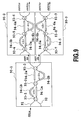
- Fig. 9 shows the circuit configuration of a conventional optical demultiplexer.
- the demultiplexer has two-stage optical demultiplexer elements 90-1, 90-2, and 90-3 connected together in tandem in two stages and having optical path length differences of 1:-2, 1:-2, and -1:2, respectively.
- the optical path length of difference is normalized a unit path length difference ⁇ L.
- the positive optical path length difference is defined to mean that in the two arms of each Mach-Zehnder circuit, the upper arm has a larger optical path length than the lower arm.
- the negative optical path length difference is defined to mean that the lower arm has a larger optical path length than the upper arm.
- the two two-stage optical demultiplexer elements 90-2 and 90-3 are disposed.
- the two-stage optical demultiplexer elements 90-1, 90-2, and 90-3 are constructed in a two-stage Mach-Zehnder form using three directional couplers 93-1 to 93-9 for each element.
- Phase shifters 94-1 to 94-6 are installed on each optical path to control phase.
- a wavelength multiplex signal of an equi-channel spacing ⁇ 1, ⁇ 2, ..., ⁇ M (M is an integer equal to or larger than 2) is input from an input port IN1a of the two-stage optical demultiplexer element 90-1 in the 1st stage, a wavelength multiplex signal of ⁇ 1, ⁇ 3, ..., ⁇ M-1 is output from one selected output port OUT2c of the two-stage optical demultiplexer element 90-2 in the 2nd stage, while a wavelength multiplex signal of ⁇ 2, ⁇ 4, ..., ⁇ M is output from one selected output port OUT4c of the two-stage optical demultiplexer element 90-3 in the 2nd stage.
- the through output port (that is, the output port having its optical waveguide physically coupled to the corresponding input port) OUT2c of the two-stage optical demultiplexer element 90-2 is selected, the optical demultiplexer element 90-2 being connected to the through output port OUT1b of the two-stage optical demultiplexer element 90-1 in the 1st stage.
- the cross output port (that is, the output port not having its optical waveguide physically coupled to the corresponding input port) OUT4c of the two-stage optical demultiplexer element 90-3 is selected, the optical demultiplexer element 90-3 being connected to the cross output port OUT2b of the two-stage optical demultiplexer element 90-2 in the 1st stage.
- the output ports are selected so that the 1st stage through output port and the 2nd stage through output port are combined together and the 1st stage cross output port and the 2nd stage cross output port are combined together.
- the output ports are thus selected because group delays in the 1st and 2nd stages offset each other to obtain zero group delay characteristics. Furthermore, even with a fabrication error in the single optical multiplexer or demultiplexer, the offset of the group delays serves to maintain substantially zero group delays. Thus, the conventional optical multiplexer or demultiplexer is characterized in that the group delay characteristics are unlikely to be affected by fabrication errors in the circuit.
- the group delay characteristics of the conventional optical multiplexer or demultiplexer is unlikely to be affected by fabrication errors in the circuit and are thus substantially zero, its transmission characteristics are prone to be affected by fabrication errors.
- a problem of the conventional optical multiplexer or demultiplexer is that a good stopband value is not obtained in the presence of a fabrication error.
- optical multiplexer or demultiplexer When the optical multiplexer or demultiplexer is actually used, group delays have only to be maintained at a certain allowable value or less, and the optical multiplexer or demultiplexer element often needs to have as good transmission characteristics as possible.
- an optical demultiplexer comprising 2-input and 2-output (hereinafter referred to as the "2x2") optical demultiplexer elements composed of optical couplers that couple two optical waveguides together at N+1 locations (N is an integer equal to or larger than 2), each the 2x2 optical demultiplexer element having a through output port and a cross output port for a single input port, in which a through output port of a first 2x2 optical demultiplexer element is connected to an input port of a second 2x2 optical demultiplexer element and a cross output port of the first 2x2 optical demultiplexer element is connected to an input port of a third 2x2 optical demultiplexer element, so that if a wavelength multiplex signal of a specified wavelength interval of ⁇ 1, ⁇ 2, ..., ⁇ M (M is an integer equal to or larger than 2) is input to an input port of the first 2x2 optical demultiplexer element, a wavelength multiplex signal of ⁇ 1, ⁇ 3, ...
- M is an integer equal to
- ⁇ M-1 is output from a selected output port of the second 2x2 optical demultiplexer element, while a wavelength multiplex signal of ⁇ 2, ⁇ 4, ... , ⁇ M is output from a selected output port of the third 2x2 optical demultiplexer element, wherein a cross output port of the second 2x2 optical demultiplexer element is selected, and a through output port of the third 2x2 optical demultiplexer element is selected, wherein the through output port of the first 2x2 optical demultiplexer element has a passband equal to that of the cross output port of the second 2x2 optical demultiplexer element, and the cross output port of the first 2x2 optical demultiplexer element has a passband equal to that of the through output port of the third 2x2 optical demultiplexer element, and wherein the through output port of the first 2x2 optical demultiplexer element has group delay characteristics opposite to those of the cross output port of the second 2x2 optical demultiplexer element, and the cross output port of the first 2x2 optical de
- selection of the output ports eliminates differences in characteristics between the input port and the two output ports which differences result from a fabrication error in the circuit, thereby minimizing fabrication errors in transmission characteristics and maintaining group delay dispersions at an allowable value or less.
- an optical multiplexer comprising 2-input and 2-output (hereinafter referred to as the "2x2") optical multiplexer elements composed of optical couplers that couple two optical waveguides together at N+1 locations (N is an integer equal to or larger than 2), each the 2x2 optical multiplexer element having a through output port and a cross output port for a single input port, in which an output port of a first 2x2 optical multiplexer element is connected to a through input port of a third 2x2 optical multiplexer element and an output port of a second 2x2 optical multiplexer element is connected to a cross input port of the third 2x2 optical multiplexer element, so that if a wavelength multiplex signal of a specified wavelength interval of ⁇ 1, ⁇ 3, ..., ⁇ M-1 (M is an integer equal to or larger than 2) is input to a selected input port of the first 2x2 optical multiplexer element, while a wavelength multiplex signal of a specified wavelength interval of ⁇ 2, ⁇ 4, ..., ⁇ M is
- ⁇ M is output from the output port of the third 2x2 optical multiplexer element, wherein a cross input port of the first 2x2 optical multiplexer element is selected, and a through input port of the second 2x2 optical multiplexer element is selected, wherein the through output port of the third 2x2 optical multiplexer element has a passband equal to that of the cross output port of the first 2x2 optical multiplexer element, and the cross output port of the third 2x2 optical multiplexer element has a passband equal to that of the through output port of the second 2x2 optical multiplexer element, and wherein the through output port of the third 2x2 optical multiplexer element has group delay characteristics opposite to those of the cross output port of the first 2x2 optical multiplexer element, and the cross output port of the third 2x2 optical multiplexer element has group delay characteristics opposite to those the through output port of the second 2x2 optical multiplexer element.
- selection of the input ports eliminates differences in characteristics between the two input ports and the output port which differences result from a fabrication error in the circuit, thereby minimizing fabrication errors in transmission characteristics and maintaining group delay dispersions at an allowable value or less.
- Fig. 1 shows the circuit configuration of an optical demultiplexer according to a first embodiment of the present invention.
- Optical demultiplexer elements 10-1, 10-2, and 10-3 have a two-stage Mach-Zehnder configuration having optical path length differences of 1:-2, -1:2, and 1:-2, respectively.
- the positive optical path length difference is defined to mean that in the two arms of each Mach-Zehnder circuit, the upper arm has a larger optical path length than the lower arm.
- the negative optical path length difference is defined to mean that the lower arm has a larger optical path length than the upper arm.
- optical couplers are directional couplers.
- Directional couplers 13-1, 13-4, and 13-7 are 3dB couplers.
- Directional couplers 13-2, 13-5, and 13-8 have the same coupling ratio, while directional couplers 13-3, 13-6, and 13-9 have the same coupling ratio.
- Phase shifters 14-1 to 14-6 are installed on each optical path to control phase.
- the phase shifter 14-1 changes the refractive index of either a waveguide 14-1a or a waveguide 14-1b to provide a phase difference to signal light passing through each waveguide.
- An optical demultiplexer is composed of optical demultiplexer elements 10-1, 10-2, and 10-3 connected together in tandem in two stages so that the one optical demultiplexer element 10-1 is disposed in the 1st stage, while the two optical demultiplexer elements 10-2 and 10-3 are disposed in the 2nd stage.
- the optical demultiplexer element 10-2 has an optical path length difference of -1:2, while the optical demultiplexer elements 10-1 and 10-3 have the opposite optical path length difference of 1:-2.
- the two phase shifters 14-1 and 14-2 of the optical demultiplexer element 10-1 in the 1st stage have a phase amount of zero.
- the phase shifters 14-3 and 14-5 of the optical demultiplexer elements 10-2 and 10-3, respectively, in the 2nd stage have a phase amount of ⁇ , and the phase shifters 14-4 and 14-6 have a phase amount of zero.
- the phase shifters 14-3 and 14-5 have a phase amount of ⁇ in order to cause the transmission characteristics of the optical demultiplexer elements 10-2 and 10-3 in the 2nd stage to deviate from the transmission characteristics of the optical demultiplexer element 10-1 by half a period.
- the passband of a through output port of the optical demultiplexer element 10-1 can be matched with the passband of a cross output port of the optical demultiplexer element 10-2. Further, the passband of a cross output port of the optical demultiplexer element 10-1 can be matched with the passband of a through output port of the optical demultiplexer element 10-3.
- the cross output port OUT1c is selected for output, the optical demultiplexer element 10-2 being connected to the through output OUT1b of the optical demultiplexer element 10-1 in the 1st stage.
- the cross output port OUT3c is selected for output, the optical demultiplexer element 10-3 being connected to the cross output port OUT2b of the optical demultiplexer element 10-1 in the 1st stage.
- Fig. 2 is a view showing the circuit configuration of an optical multiplexer according to the first embodiment of the present invention.
- Optical multiplexer elements 20-1, 20-2, and 20-3 have a two-stage Mach-Zehnder configuration having optical path length differences of 2:-1, -2:1, and -2:1, respectively.
- Directional couplers 23-1, 23-4, and 23-7 are 3dB couplers.
- Directional couplers 23-2, 23-5, and 23-8 have the same coupling ratio, while directional couplers 23-3, 23-6, and 23-9 have the same coupling ratio.
- Phase shifters 24-1 to 24-6 are installed on each optical path to control phase.
- An optical multiplexer is composed of optical multiplexer elements 20-1, 20-2, and 20-3 connected together in tandem in two stages so that the two optical multiplexer elements 20-1 and 20-2 are disposed in the 1st stage, while the one optical multiplexer element 20-3 is disposed in the 2nd stage.
- the optical multiplexer element 20-1 has an optical path length difference of 2:-1, whereas the optical multiplexer elements 20-2 and 20-3 have the opposite optical path length difference of -1:2.
- the two phase shifters 24-1 and 24-2 of the optical multiplexer element 20-3 in the 2nd stage have a phase amount of zero.
- the phase shifters 24-3 and 24-5 of the optical multiplexer elements 20-1 and 20-2, respectively, in the 1st stage have a phase amount of ⁇ , and the phase shifters 24-4 and 24-6 have a phase amount of zero.
- the phase shifters 24-3 and 24-5 have a phase amount of ⁇ in order to cause the transmission characteristics of the optical multiplexer elements 20-1 and 20-2 in the 1st stage to deviate from the transmission characteristics of the optical multiplexer element 20-3 by half a period.
- the passband of a through output port of the optical multiplexer element 20-3 can be matched with the passband of a cross output port of the optical multiplexer element 20-1. Further, the passband of a cross output port of the optical multiplexer element 20-3 can be matched with the passband of a through output port of the optical multiplexer element 20-2.
- the cross input port INla is selected for input, the optical multiplexer element 20-1 being connected to the through output IN1b of the optical multiplexer element 20-3 in the 2nd stage.
- the cross input port IN3a is selected for input, the optical multiplexer element 20-2 being connected to the cross input port IN2b of the optical multiplexer element 20-3 in the 2nd stage.
- optical demultiplexer and the optical multiplexer are similarly described, and thus only the optical demultiplexer will be described below.
- the present invention is not limited to the optical demultiplexer, but the description of the optical demultiplexer is similarly applicable to the optical multiplexer.
- the optical multiplexer elements as components have an optical path length difference of 1:-2, but arbitrary optical multiplexer elements of an optical path length difference of ⁇ 1: ⁇ 2 (the symbol ⁇ hereinafter indicates that either + or - is to be selected) can be produced by varying the coupling ratios of the directional couplers or the phase amounts of the phase shifters.
- the circuit configuration is the same as that in the two stage configuration, but the optical path length difference is ⁇ 1: ⁇ 2: ⁇ 2: ... : ⁇ 2. Further, for the three-stage configuration, the optical path length difference may be ⁇ 1: ⁇ 2: ⁇ 4.
- the optical demultiplexer element 10-1 in the 1st stage and the optical demultiplexer elements 10-2 and 10-3 in the 2nd stage are of the same type except for the phase amounts of the phase shifters.
- optical demultiplexer elements having different filter characteristics may be used so that the 1st stage is composed of a maximally flat filter and the 2nd stage is composed of a filter having equi-ripple characteristics in the passband and stopband.
- a transfer function G 1 (z) is set between the input port IN1a and through output port OUT1b of the optical demultiplexer element 10-1.
- a transfer function H 1 (z) is set between the input port IN1a and cross output port OUT2b of the optical demultiplexer element 10-1.
- the transfer function between the through output port OUT1b of the optical demultiplexer element 10-1 and the cross output port OUT1c of the optical demultiplexer element 10-2 is represented as H 2 (-z)
- the transfer function between the input port IN1a of the optical demultiplexer element 10-1 and the cross output port OUT1c of the optical demultiplexer element 10-2 is represented as G 1 (z)H 2 (-z).
- the subscripts 1 and 2 of the transfer functions represent the 1st and 2nd stages, respectively.
- -z represents a deviation by half a period as is apparent from the definition of z.
- the phase shifters 14-3 and 14-5 of the optical demultiplexer elements 10-2 and 10-3, respectively, in the 2nd stage the characteristics of the optical demultiplexer element 10-2 deviate from the characteristics of the optical demultiplexer element 10-3 by half a period, and the transfer function is a function of -z.
- the characteristics of the optical demultiplexer element 10-2 thus deviate from the characteristics of the optical demultiplexer element 10-3 in order to match the passband of the through output port of the optical demultiplexer element 10-1 in the 1st stage with the passband of the cross output port of the optical demultiplexer element 10-2 in the 2nd stage and to match the passband of the cross output port of the optical demultiplexer element 10-1 in the 1st stage with the passband of the through output port of the optical demultiplexer element 10-3 in the 2nd stage.
- the optical demultiplexer elements 10-2 and 10-3 in the 2nd stage use the same directional couplers as those in the 1st stage to cause phase to deviate by ⁇ using Mach-Zehnder circuits having an optical path length difference of 1. Accordingly, the transmission characteristics of the optical demultiplexer elements 10-2 and 10-3 in the 2nd stage deviate from the transmission characteristics of the optical demultiplexer element 10-1 in the 1st stage by half a period. That is, the transfer functions for the optical demultiplexer elements 10-2 and 10-3 in the 2nd stage are obtained by subjecting the transfer function for the optical demultiplexer element 10-1 in the 1st stage to z ⁇ -z conversion.
- the transfer function between the 1st stage through output port and the 2nd stage cross output port becomes equal to the transfer function between the 1st stage cross output port and the 2nd stage through output port, which otherwise deviates therefrom by half pitch, in other words, the characteristics between the 1st stage through output port and the 2nd stage cross output port become equal to the characteristics between the 1st stage cross output port and the 2nd stage through output port, which otherwise deviate therefrom by half pitch.
- the relational expression of Equation 1 indicates that the through characteristics G(z) of the optical demultiplexer elements equal the cross characteristics H * (-z) thereof, which have group delay characteristics opposite to those of the through output port and deviate therefrom by half a period.
- the transmission characteristics of the through and cross output ports are set to have opposite group delay characteristics in order to cause the group delay characteristics of a signal passing through the 1st stage through output port and the 2nd stage cross output port to offset the group delay characteristics of a signal passing through the 1st stage cross output port and the 2nd stage through output port, vice versa.
- the transfer function G(z)H(-z) between the 1st stage through output port and the 2nd stage cross output port is G(z)G * (z)
- the transfer function H(z)G(-z) between the 1st stage cross output port and the 2nd stage through output port is G * (-z)G(-z).
- the 1st stage cross output port has transmission characteristics G * (-z), while the 2nd stage through output port has transmission characteristics G(-z), that is, inverse group delay characteristics.
- G * (-z)
- G(-z) transmission characteristics
- the offset effect makes the group delay characteristics zero for both the characteristics between the 1st stage through output port and the 2nd stage cross output port and between the 1st stage cross output port and the 2nd stage through cross output port.
- the characteristics between the 1st stage through output port and the 2nd stage cross output port become equal to the characteristics between the 1st stage cross output port and the 2nd stage through cross output port, which otherwise deviate therefrom by half a period.
- the through output port of the optical demultiplexer element has transmission characteristics different from those of the cross output port thereof.
- the optical demultiplexer of the present invention is not affected by fabrication errors because the difference in transmission characteristics between the through output port and cross output port of the optical demultiplexer element resulting from a fabrication error is uniformly distributed by passage through the 1st stage through output port and the 2nd stage cross output port and passage through the 1st stage cross output port and the 2nd stage through output port.
- the conventional optical demultiplexer shown in Fig. 9 will be similarly considered.
- the conventional optical demultiplexer has such a circuit configuration that the 1st stage through output port is connected to the 2nd stage through output port, whereas the 1st stage cross output port is connected to the 2nd stage cross output port.
- the same optical demultiplexer elements are used in both the 1st and 2nd stages.
- the transfer function (IN1a ⁇ OUT1b ⁇ OUT2c) between the 1st stage through output port and the 2nd stage through output port is G(z)G * (z)
- the transfer function (IN1a ⁇ OUT2b ⁇ OUT4c) between the 1st stage cross output port and the 2nd stage cross output port is H(z)H * (z).
- the characteristics between the 1st stage through output port and the 2nd stage through output port become equal to characteristics between the 1st stage cross output port and the 2nd stage cross output port by half a period. That is, in the optical demultiplexer elements, the difference between the characteristics between the 1st stage through output port and 2nd stage through output port and the characteristics between the 1st stage cross output port and the 2nd stage cross output port which difference results from a fabrication error tends to be increased by passage through the 1st stage through output port and the 2nd stage through output port and passage through the 1st stage cross output port and the 2nd stage cross output port. This is why the conventional optical demultiplexer is prone to be affected by fabrication errors.
- the conventional optical demultiplexer is advantageous in that the group delays are always zero.
- the difference between the transmission characteristics of the through output port and the transmission characteristics of the cross output port which difference results from the fabrication error tends to be increased by passage through the 1st stage through output port and the 2nd stage through output port and passage through the 1st stage cross output port and the 2nd stage cross output port. Therefore, the conventional optical demultiplexer is prone to be affected by fabrication errors.
- the optical demultiplexer according to the present invention even with a fabrication error, the difference between the transmission characteristics of the through output port and the transmission characteristics of the cross output port which difference results from the fabrication error is uniformly distributed by passage through the 1st stage through output port and the 2nd stage through output port and passage through the 1st stage cross output port and the 2nd stage cross output port. Consequently, the present optical demultiplexer is unlikely to be affected by fabrication errors.
- the group delay characteristics are essentially not zero, but when the through and cross output ports of the optical demultiplexer element have opposite group delay characteristics, the offset effect between the 1st and 2nd stage group delay characteristics causes the group delay characteristics to approximate to zero.
- the offset effect between the 1st and 2nd stage group delay characteristics is most significant under the interleave filter condition (no fabrication errors), and in this case, the group delay is substantially zero.
- the optical demultiplexer shown in Fig. 1 was produced using a silica-based planar lightwave circuit.
- a 4-inch Si wafer was used as a substrate, and a desired circuit pattern was formed by using a flame hydrolysis deposition (FHD) technique and a reactive ion etching technique.
- Heaters fabricated above waveguides were activated to adjust the phase amount on the basis of thermooptic effects.
- Optical demultiplexer elements were designed to have equi-ripple characteristics both in the passband and in the stopband.
- Directional couplers in the three optical demultiplexer element had the same coupling ratios.
- the coupling ratios of the directional couplers of the optical demultiplexer elements were, from the input port side, 50% for 13-1, 13-4, and 13-7, 34.8% for 13-2, 13-5, and 13-8, and 9.6% for 13-3, 13-6, and 13-9.
- the two phase shifters in the 1st stage optical demultiplexer element had a phase amount of zero.
- the phase shifter 14-3 and 14-5 had a phase amount of ⁇
- the phase shifter 14-4 and 14-6 had a phase amount of 0.
- the directional couplers were used as optical couplers, but other optical couplers such as MMI (Multi Mode Interference) couplers may be used.
- the optical demultiplexer was produced using the silica-based planar lightwave circuit, but the circuit may be produced using other materials such as SiO N .
- the optical waveguides may be producing using optical fibers as well as the planar lightwave circuit.
- the heaters utilizing thermooptic effects were used as phase shifters, but the phase shifters may be based on other principles such as electro-optic effects.
- the present invention relates to the circuit configuration of the optical demultiplexer and is not restricted to implementing means therefor.
- the circuit parameters used in the present invention are designed values and may vary depending on design conditions. Therefore, the present invention is not restricted to the circuit parameters.
- phase shifter are implemented as heating effected by the heaters and allow the shift amounts thereof to be variably set, so that the phase shift amount is not considered to be a fabrication error factor.
- the optical demultiplexer was intentionally produced to have an error in coupling ratio in order to check its dependency on fabrication errors.
- Fig. 3A shows the results of measurements of the transmission characteristics of the optical demultiplexer according to the first embodiment of the present invention. These are the results of examination of the transmission characteristics obtained when the coupling ratios of all the directional couplers of the optical demultiplexer were reduced by about 0, 5, and 10%.
- Fig. 3B shows the results of measurements of the transmission characteristics of a conventional optical demultiplexer. For comparison, the conventional optical demultiplexer shown in Fig. 9 was produced to check its dependency on fabrication errors.
- Period frequency was 100 GHz.
- the variation of the transmission characteristics (hereinafter simply referred to as the "through cross transmission characteristics") between the 1st stage through output port and the 2nd stage cross output port (IN1a ⁇ OUT1b ⁇ OUT1c) in response to a fabrication error is comparable to the variation of the transmission characteristics (hereinafter simply referred to as the "cross through transmission characteristics") between the 1st stage cross output port and the 2nd stage through output port (IN1a ⁇ OUT2b ⁇ OUT3c) in response to a fabrication error.
- the stopband has a stop value of about -22dB.
- the transmission characteristics (hereinafter simply referred to as the "cross cross transmission characteristics") between the 1st stage cross output port and the 2nd stage cross output port (IN1a ⁇ OUT2b ⁇ OUT4c) do not substantially vary even with a fabrication error, but the transmission characteristics (hereinafter simply referred to as the “through through transmission characteristics”) between the 1st stage through output port and the 2nd stage through output port (IN1a ⁇ OUT1b ⁇ OUT2c) vary sharply.
- the stopband for the through through transmission characteristics has a stop value of about -10dB.
- the difference between the through through transmission characteristics and the cross cross transmission characteristics caused by a fabrication error is associated with a difference in the dependency on fabrication errors between the transmission characteristics of the through output port and the transmission characteristics of the cross output port thereof the optical demultiplexer element, which is a component of the optical demultiplexer.
- the coupling ratios of the directional couplers deviate in the same direction, for example, all the coupling ratios decrease, then the stop value of the transmission characteristics of the through output port of the optical demultiplexer element is degraded, but the fabrication error in the transmission characteristics of the cross output port does not vary significantly.
- the conventional optical demultiplexer in the case of the through through transmission characteristics, fabrication errors are accumulated to become gross.
- a gross fabrication error in the transmission characteristics of the through output port is uniformly distributed to the through cross transmission characteristics and to the cross through transmission characteristics, thereby hindering a generally gross fabrication error in transmission characteristics.
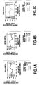
- Figs. 4A-4F show the results of measurements of the group delay dispersion characteristics of the optical demultiplexer according to the first embodiment of the present invention.
- the conventional optical demultiplexer employs a configuration that automatically zeroes group delay dispersion, but the optical demultiplexer according to this embodiment is designed so that the group delay dispersion is offset between the 1st stage and the 2nd stage.
- Figs. 4A-4F also show the results of measurements of the group delay dispersion of each optical demultiplexer element.
- the group delay dispersion (IN1a ⁇ OUT1b) in the through output port of the optical demultiplexer element 10-1 in the 1st stage has characteristics opposite to those of the group delay dispersion (OUT1b ⁇ OUT1c) in the cross output port of the optical demultiplexer element 10-2 in the 2nd stage. Accordingly, without a fabrication error, the through cross group delay dispersion in the entire optical demultiplexer becomes substantially zero.
- the group delay dispersion (IN1a ⁇ OUT2b) in the cross output port of the optical demultiplexer element 10-1 in the 1st stage has characteristics opposite to those of the group delay dispersion (OUT2b ⁇ OUT3c) in the through output port of the optical demultiplexer element 10-3 in the 2nd stage. Accordingly, without a fabrication error, the group delay dispersion in IN1a ⁇ OUT2b ⁇ OUT3c (hereinafter simply referred to as the "cross through group delay”) becomes substantially zero.
- both the group delay dispersion in the through output port of the optical demultiplexer element 10-1 in the 1st stage and the group delay dispersion in the cross output port of the optical demultiplexer element 10-2 in the 2nd stage deviate from their opposite characteristics, so that the grosser the fabrication error becomes, the more the through cross group delay dispersion in the entire optical demultiplexer deviates from zero.
- the maximum value of the group delay dispersion associated with fabrication errors is about 50ps/nm even for a coupling ratio error of 10%. This value is substantially equivalent to the group delay dispersion in a single optical demultiplexer element having no fabrication error, and is not so large.
- circuit configuration of the optical demultiplexer shown in Fig. 1 has basically been described.
- the present invention is not limited to the circuit configuration in Fig. 1, so that other embodiments will be mentioned below.
- Fig. 5 is a view showing the circuit configuration of an optical demultiplexer according to a second embodiment of the present invention.
- This circuit configuration differs from that of the optical demultiplexer shown in Fig. 1 in the optical path length differences in an optical demultiplexer element 50-2 and an optical demultiplexer element 50-3.
- the optical path length differences in the optical demultiplexer element 50-2 and the optical demultiplexer element 50-3 are each -2:1.
- Directional couplers 53-6, 53-5, and 53-4 in the optical demultiplexer element 50-2 in Fig. 5 correspond to the directional couplers 13-4, 13-5, and 13-6 in Fig. 1.
- Directional couplers 53-9, 53-8, and 53-7 in the optical demultiplexer element 50-3 in Fig. 5 correspond to the directional couplers 13-7, 13-8, and 13-9 in Fig. 1.
- phase shifters 54-4 and 54-3 in the optical demultiplexer element 50-2 in Fig. 5 correspond to the phase shifters 14-3 and 14-4 in Fig. 1.
- Phase shifters 54-6 and 54-5 in the optical demultiplexer element 50-3 in Fig. 5 correspond to the phase shifters 14-5 and 14-6 in Fig. 1.
- the optical demultiplexer element 50-2 in Fig. 5 is obtained by subjecting the optical demultiplexer element 10-2 in Fig. 1 to a symmetry operation so as to have an optical path length difference of -2:1.
- the optical demultiplexer element 50-3 in Fig. 5 is obtained by subjecting the optical demultiplexer element 10-3 in Fig. 1 to a symmetry operation so as to have an optical path length difference of -2:1.
- Figs. 6A-6D show a transfer function matrix for a circuit configuration obtained through a symmetry operation. Now, Figs. 6A-6D will be referenced to show that the circuit configuration meets the requirements of the present invention.
- the through cross transmission characteristics (IN1a ⁇ OUT1b ⁇ OUT1c) are expressed as the product of the transmission characteristics (IN1a ⁇ OUT1b)G(z) of the through output port of the optical demultiplexer element 50-1 and the transmission characteristics (OUT1b ⁇ OUT1c)H(-z) of the cross output port of the optical demultiplexer element 50-2.
- the through cross transmission characteristics (IN1a ⁇ OUT1b ⁇ OUT1c) is G(z)H(-z).
- the cross through transmission characteristics (IN1a ⁇ OUT2b ⁇ OUT3c) are expressed as the product of the transmission characteristics (IN1a ⁇ OUT2b)H(z) of the cross output port of the optical demultiplexer element 50-1 and the transmission characteristics (OUT2b ⁇ OUT3c)G(-z) of the through output port of the optical demultiplexer element 50-3.
- the cross through transmission characteristics (IN1a ⁇ OUT2b ⁇ OUT3c) is H(z)G(-z).
- the transmission characteristics (IN1a ⁇ OUT1b) of the through output port of the optical demultiplexer element 50-1 are represented as G(z)
- the transmission characteristics (OUT1b ⁇ OUT1c) of the cross output port of the optical demultiplexer element 50-2 is represented as G * (z).
- the former has group delay characteristics opposite to those of the latter.
- the transmission characteristics (IN1a ⁇ OUT2b) of the cross output port of the optical demultiplexer element 50-1 are represented as G * (-z)
- the transmission characteristics (OUT2b ⁇ OUT3c) of the through output port of the optical demultiplexer element 50-3 is represented as G(-z). This also indicates that the former has group delay characteristics opposite to those of the latter.
- the through cross transmission characteristics (IN1a ⁇ OUT1b ⁇ OUT1c) for the entire optical demultiplexer are G(z)G * (z), and the cross through transmission characteristics therefor is G * (-z)G(-z). Consequently, the group delay characteristics for the former offset the group delay characteristics for the latter, resulting in zero group delay dispersion.
- Fig. 7 shows the circuit configuration of an optical demultiplexer according to a third embodiment of the present invention.
- a 1st stage output port is connected to a 2nd stage cross output port
- a 1st stage cross output port is connected to a 2nd stage through output port.
- the through cross transmission characteristics (IN1a ⁇ OUT1b ⁇ OUT1c) are expressed as the product of the transmission characteristics (IN1a ⁇ OUT1b)G * (z) of the through output port of the optical demultiplexer element 70-1 and the transmission characteristics (OUT1b ⁇ OUT1c)H * (-z) of the cross output port of the optical demultiplexer element 70-2.
- the transmission characteristics (IN1a ⁇ OUT1b) of the through output port of the optical demultiplexer element 70-1 are represented as G * (z)
- the transmission characteristics (OUT1b ⁇ OUT1c) of the cross output port of the optical demultiplexer element 70-2 is represented as G(z). That is, the former has group delay characteristics opposite to those of the latter. Therefore, the through cross transmission characteristics (IN1a ⁇ OUT1b ⁇ OUT1c) is G * (z)G(z), resulting in zero group delay dispersion.
- the cross through transmission characteristics (IN1a ⁇ OUT2b ⁇ OUT3c) are expressed as the product of the transmission characteristics (IN1a ⁇ OUT2b)H(z) of the through output port of the optical demultiplexer element 70-1 and the transmission characteristics (OUT2b ⁇ OUT3c)G(-z) of the cross output port of the optical demultiplexer element 70-3.
- the transmission characteristics (IN1a ⁇ OUT2b) of the cross output port of the optical demultiplexer element 70-1 are represented as G * (-z)
- the transmission characteristics (OUT2b ⁇ OUT3c) of the through output port of the optical demultiplexer element 70-3 is represented as G(z). That is, the former has group delay characteristics opposite to those of the latter. Therefore, the cross through transmission characteristics (IN1a ⁇ OUT2b ⁇ OUT3c) is G * (-z)G(-z), resulting in zero group delay dispersion.
- circuit configuration meeting the requirements of the present invention is not limited to the one shown in Fig. 1, but a plurality of such circuit configurations exist, including the ones shown in Figs. 5 and 7.
- the first embodiment is designed so that all the optical demultiplexer elements have equi-ripple characteristics in the stopband and passband.
- the optical demultiplexer according to the present invention not all the optical demultiplexer elements have the same characteristics. The case will be described in which the optical demultiplexer element in the 1st stage has the maximally flat transmission characteristics, whereas the two optical demultiplexer elements in the 2nd stage have equi-ripple characteristics.
- the optical demultiplexer elements of this circuit have a two-stage Mach-Zehnder configuration.
- the coupling ratios of the directional couplers in the 1st stage optical demultiplexer element having maximally flat characteristics are, from the input port side, 50, 25, and 6.7%.
- the coupling ratios of the directional couplers in the 2nd stage optical demultiplexer element having equi-ripple characteristics are, from the input port side, 50, 34.8, and 9.6%.
- the optical path length differences and the phase amounts of the phase shifters are similar to those in the circuit configuration shown in Fig. 1.
- the connections of the input and output ports are also similar to those shown in Fig. 1.
- Fig. 8A shows the results of measurements of the transmission characteristics of an optical demultiplexer according to a fourth embodiment of the present invention.
- Fig. 8B shows the results of measurements of the through cross group delay dispersion characteristics of the optical demultiplexer according to the fourth embodiment of the present invention.
- Fig. 8C shows the results of measurements of the cross through group delay dispersion characteristics of the optical demultiplexer according to the fourth embodiment of the present invention.
- This embodiment is designed so that the optical demultiplexer element in the 1st stage has maximally flat transmission characteristics, while the two optical demultiplexer elements in the 2nd stage have equi-ripple transmission characteristics. These different characteristics are selected so as to suppress the stop value for the stopband area, one of the transmission characteristics. Without any fabrication error (the coupling ratio error is 0%) as shown in Fig. 8A, the stop value is about -46 dB. Since the optical demultiplexer of the first embodiment shown in Fig. 3A has a stop value of about -32 dB, the fourth embodiment provides a significantly suppressed stop value.
- the optical demultiplexer elements in the 1st and 2nd stages having different transmission characteristics are combined to successfully remove a mountain of transmission in the center of the stopband, shown in Fig. 3A.
- the connections in Fig. 1 are also employed to uniformly distribute a fabrication error to the through cross transmission characteristics and to the cross through transmission characteristics.
- the group delay dispersion is not zero even without a fabrication error.
- the optical demultiplexer element in the 1st stage has characteristics different from those of the optical demultiplexer element in the 2nd stage.
- the through or cross output port of the optical demultiplexer element in the 1st stage basically has group delay dispersion substantially opposite to those of the through or cross output port of the optical demultiplexer element in the 2nd stage, so that the group delay dispersions in the 1st and 2nd stages offset each other.
- the group delay dispersion value is small though not zero.
- the maximum group delay dispersion is about 60ps/nm and is not so significant.
- the deviation of the characteristics of the circuit caused by a fabrication error can be distributed to the transmission characteristics and to the group delay characteristics to maintain the group delay characteristics at an allowable value or less, thereby maintaining good transmission characteristics.
Landscapes
- Physics & Mathematics (AREA)
- General Physics & Mathematics (AREA)
- Optics & Photonics (AREA)
- Engineering & Computer Science (AREA)
- Chemical & Material Sciences (AREA)
- Dispersion Chemistry (AREA)
- Computer Networks & Wireless Communication (AREA)
- Signal Processing (AREA)
- Microelectronics & Electronic Packaging (AREA)
- Optical Integrated Circuits (AREA)
- Optical Communication System (AREA)
Abstract
Description
Claims (2)
- An optical demultiplexer comprising 2-input and 2-output (hereinafter referred to as the "2x2") optical demultiplexer elements composed of optical couplers that couple two optical waveguides together at N+1 locations (N is an integer equal to or larger than 2), each said 2x2 optical demultiplexer element having a through output port and a cross output port for a single input port,
in which a through output port of a first 2x2 optical demultiplexer element is connected to an input port of a second 2x2 optical demultiplexer element and a cross output port of said first 2x2 optical demultiplexer element is connected to an input port of a third 2x2 optical demultiplexer element,
so that if a wavelength multiplex signal of a specified wavelength interval of λ1, λ2, ..., λM (M is an integer equal to or larger than 2) is input to an input port of said first 2x2 optical demultiplexer element, a wavelength multiplex signal of λ1, λ3, ... , λM-1 is output from a selected output port of said second 2x2 optical demultiplexer element, while a wavelength multiplex signal of λ2, λ4, ... , λM is output from a selected output port of said third 2x2 optical demultiplexer element,
wherein a cross output port of said second 2x2 optical demultiplexer element is selected, and a through output port of said third 2x2 optical demultiplexer element is selected,
wherein the through output port of said first 2x2 optical demultiplexer element has a passband equal to that of the cross output port of said second 2x2 optical demultiplexer element, and the cross output port of said first 2x2 optical demultiplexer element has a passband equal to that of the through output port of said third 2x2 optical demultiplexer element, and
wherein the through output port of said first 2x2 optical demultiplexer element has group delay characteristics opposite to those of the cross output port of said second 2x2 optical demultiplexer element, and the cross output port of said first 2x2 optical demultiplexer element has group delay characteristics opposite to those the through output port of said third 2x2 optical demultiplexer element. - An optical multiplexer comprising 2-input and 2-output (hereinafter referred to as the "2x2") optical multiplexer elements composed of optical couplers that couple two optical waveguides together at N+1 locations (N is an integer equal to or larger than 2), each said 2x2 optical multiplexer element having a through output port and a cross output port for a single input port,
in which an output port of a first 2x2 optical multiplexer element is connected to a through input port of a third 2x2 optical multiplexer element and an output port of a second 2x2 optical multiplexer element is connected to a cross input port of said third 2x2 optical multiplexer element,
so that if a wavelength multiplex signal of a specified wavelength interval of λ1, λ3, ..., λM-1 (M is an integer equal to or larger than 2) is input to a selected input port of said first 2x2 optical multiplexer element, while a wavelength multiplex signal of a specified wavelength interval of λ2, λ4, ..., λM is input to a selected input port of said second 2x2 optical multiplexer element, then a wavelength multiplex signal of λ1, λ2, ... , λM is output from the output port of said third 2x2 optical multiplexer element,
wherein a cross input port of said first 2x2 optical multiplexer element is selected, and a through input port of said second 2x2 optical multiplexer element is selected,
wherein the through output port of said third 2x2 optical multiplexer element has a passband equal to that of the cross output port of said first 2x2 optical multiplexer element, and the cross output port of said third 2x2 optical multiplexer element has a passband equal to that of the through output port of said second 2x2 optical multiplexer element, and
wherein the through output port of said third 2x2 optical multiplexer element has group delay characteristics opposite to those of the cross output port of said first 2x2 optical multiplexer element, and the cross output port of said third 2x2 optical multiplexer element has group delay characteristics opposite to those the through output port of said second 2x2 optical multiplexer element.
Applications Claiming Priority (2)
| Application Number | Priority Date | Filing Date | Title |
|---|---|---|---|
| JP2001031483 | 2001-02-07 | ||
| JP2001031483 | 2001-02-07 |
Publications (3)
| Publication Number | Publication Date |
|---|---|
| EP1231490A2 true EP1231490A2 (en) | 2002-08-14 |
| EP1231490A3 EP1231490A3 (en) | 2004-08-18 |
| EP1231490B1 EP1231490B1 (en) | 2008-04-16 |
Family
ID=18895561
Family Applications (1)
| Application Number | Title | Priority Date | Filing Date |
|---|---|---|---|
| EP02250792A Expired - Lifetime EP1231490B1 (en) | 2001-02-07 | 2002-02-06 | Optical multiplexer and optical demultiplexer |
Country Status (3)
| Country | Link |
|---|---|
| US (1) | US6735358B2 (en) |
| EP (1) | EP1231490B1 (en) |
| DE (1) | DE60226086T2 (en) |
Cited By (3)
| Publication number | Priority date | Publication date | Assignee | Title |
|---|---|---|---|---|
| EP1426800A3 (en) * | 2002-12-06 | 2005-01-12 | Nippon Telegraph and Telephone Corporation | Optical multi/demultiplexing circuit equipped with phase generating device |
| US7555178B2 (en) | 2007-07-20 | 2009-06-30 | Infinera Corporation | Periodic optical filter |
| EP1971060A4 (en) * | 2005-11-29 | 2010-06-02 | G Uchrezhdenie Federalnoe Agen | OPTICAL MULTIPLEXER CONTROL |
Families Citing this family (12)
| Publication number | Priority date | Publication date | Assignee | Title |
|---|---|---|---|---|
| JP3802838B2 (en) * | 2001-05-30 | 2006-07-26 | 古河電気工業株式会社 | Optical multiplexer / demultiplexer |
| US7212705B2 (en) * | 2002-08-22 | 2007-05-01 | Main Street Ventures, Llc | All optical decoding systems for decoding optical encoded data symbols across multiple decoding layers |
| US6768843B1 (en) * | 2002-08-16 | 2004-07-27 | Wavesplitter Technologies, Inc. | Cascaded fourier filter interleaver having enhanced performance |
| TWI306174B (en) * | 2006-06-29 | 2009-02-11 | Ind Tech Res Inst | Optical coupler with stabilized couping ratio |
| US7630599B2 (en) * | 2007-12-14 | 2009-12-08 | Jds Uniphase Corporation | Wavelength dispersive device with temperature compensation |
| US8995836B2 (en) * | 2010-07-13 | 2015-03-31 | Futurewei Technologies, Inc. | Passive optical network with adaptive filters for upstream transmission management |
| US10050717B2 (en) * | 2015-02-19 | 2018-08-14 | Nippon Telegraph And Telephone Corporation | Multi-stage interferometer circuit with waveform shaping function |
| JP7096481B2 (en) * | 2018-02-05 | 2022-07-06 | 富士通株式会社 | Optical transmission device, optical demultiplexer, and optical demultiplexing control method |
| JP7279518B2 (en) | 2019-05-29 | 2023-05-23 | 富士通株式会社 | Optical demultiplexer, optical transmission device and optical demultiplexing control method |
| JP7688255B2 (en) * | 2021-06-28 | 2025-06-04 | 富士通株式会社 | Optical splitter and communication device |
| CA3233274A1 (en) * | 2021-09-28 | 2023-04-06 | Psiquantum, Corp. | Multiplexing for photonic circuits |
| US20230125660A1 (en) * | 2022-10-17 | 2023-04-27 | Wenhua Lin | Technologies for optical demultiplexing with backwards compatibility |
Family Cites Families (3)
| Publication number | Priority date | Publication date | Assignee | Title |
|---|---|---|---|---|
| JPH079524B2 (en) * | 1986-12-12 | 1995-02-01 | 日本電気株式会社 | Optical demultiplexer |
| US5259048A (en) * | 1991-09-30 | 1993-11-02 | Kabushiki Kaisha Toshiba | Optical equalizer |
| US5852505A (en) * | 1994-12-28 | 1998-12-22 | Lucent Technologies Inc. | Dense waveguide division multiplexers implemented using a first stage fourier filter |
-
2002
- 2002-02-04 US US10/067,065 patent/US6735358B2/en not_active Expired - Fee Related
- 2002-02-06 EP EP02250792A patent/EP1231490B1/en not_active Expired - Lifetime
- 2002-02-06 DE DE60226086T patent/DE60226086T2/en not_active Expired - Lifetime
Cited By (7)
| Publication number | Priority date | Publication date | Assignee | Title |
|---|---|---|---|---|
| EP1426800A3 (en) * | 2002-12-06 | 2005-01-12 | Nippon Telegraph and Telephone Corporation | Optical multi/demultiplexing circuit equipped with phase generating device |
| US7085438B2 (en) | 2002-12-06 | 2006-08-01 | Nippon Telegraph And Telephone Corporation | Optical multi/demultiplexing circuit equipped with phase generating device |
| EP1830207A2 (en) | 2002-12-06 | 2007-09-05 | Nippon Telegraph and Telephone Corporation | Optical multi/demultiplexing circuit equipped with phase generating device |
| EP1830207A3 (en) * | 2002-12-06 | 2007-09-12 | Nippon Telegraph and Telephone Corporation | Optical multi/demultiplexing circuit equipped with phase generating device |
| CN1508997B (en) * | 2002-12-06 | 2010-05-05 | 日本电信电话株式会社 | Optical multiplexing/demultiplexing circuits incorporating phase generating devices |
| EP1971060A4 (en) * | 2005-11-29 | 2010-06-02 | G Uchrezhdenie Federalnoe Agen | OPTICAL MULTIPLEXER CONTROL |
| US7555178B2 (en) | 2007-07-20 | 2009-06-30 | Infinera Corporation | Periodic optical filter |
Also Published As
| Publication number | Publication date |
|---|---|
| EP1231490A3 (en) | 2004-08-18 |
| EP1231490B1 (en) | 2008-04-16 |
| DE60226086D1 (en) | 2008-05-29 |
| US6735358B2 (en) | 2004-05-11 |
| US20020106147A1 (en) | 2002-08-08 |
| DE60226086T2 (en) | 2009-06-04 |
Similar Documents
| Publication | Publication Date | Title |
|---|---|---|
| EP1231490B1 (en) | Optical multiplexer and optical demultiplexer | |
| US10459168B2 (en) | Optical devices and method for tuning an optical signal | |
| US7555175B2 (en) | Arrayed waveguide grating optical multiplexer/demultiplexer | |
| WO2020210288A1 (en) | Wavelength division multiplexing filter for multiplexing or demultiplexing using cascaded frequency shaping | |
| EP1830207B1 (en) | Optical multi/demultiplexing circuit equipped with phase generating device | |
| US8781331B2 (en) | Controllable optical add/drop multiplexer | |
| US9780903B2 (en) | Optical wavelength demultiplexer having optical interference filters connected in cascade | |
| JP4822141B2 (en) | Wavelength group optical demultiplexer, wavelength group optical multiplexer, and wavelength group optical selective switch | |
| EP1857846B1 (en) | Asymmetric mach-zehnder interferometer having a reduced drive voltage coupled to a compact low-loss arrayed waveguide grating | |
| Oguma et al. | Compact and low-loss interleave filter employing lattice-form structure and silica-based waveguide | |
| JP5949610B2 (en) | Wavelength multiplexer / demultiplexer and optical integrated circuit device | |
| CN101405974B (en) | controllable optical multiplexer | |
| US6947631B2 (en) | Waveguide-type optical multiplexer/demultiplexer | |
| US20060222296A1 (en) | Optical wavelength division multiplexer | |
| US7003198B2 (en) | Integrateable band filter using waveguide grating routers | |
| US6728446B2 (en) | Compact wavelength routing device having substantially flat passband | |
| Doerr et al. | Planar lightwave circuit eight-channel CWDM multiplexer with< 3.9-dB insertion loss | |
| JP3652315B2 (en) | Optical demultiplexer and optical multiplexer | |
| JP2003315570A (en) | Optical wavelength multiplexer / demultiplexer | |
| JP3740357B2 (en) | Optical multiplexer / demultiplexer with improved group delay characteristics | |
| EP1581828B1 (en) | Integrated optical add drop device having switching function and method of switching | |
| JPH0659291A (en) | Waveguide type optical multiplexer-branching filter for four-wave multiplex transmission and eight-wave multiple transmission | |
| Jinguji et al. | Synthesis of one-input M-output optical FIR lattice circuits | |
| EP1447693A1 (en) | Flexible Passband Filter | |
| EP1122905A2 (en) | Apparatus and method for wavelength multiplexing/demultiplexing |
Legal Events
| Date | Code | Title | Description |
|---|---|---|---|
| PUAI | Public reference made under article 153(3) epc to a published international application that has entered the european phase |
Free format text: ORIGINAL CODE: 0009012 |
|
| AK | Designated contracting states |
Kind code of ref document: A2 Designated state(s): AT BE CH CY DE DK ES FI FR GB GR IE IT LI LU MC NL PT SE TR |
|
| AX | Request for extension of the european patent |
Free format text: AL;LT;LV;MK;RO;SI |
|
| PUAL | Search report despatched |
Free format text: ORIGINAL CODE: 0009013 |
|
| AK | Designated contracting states |
Kind code of ref document: A3 Designated state(s): AT BE CH CY DE DK ES FI FR GB GR IE IT LI LU MC NL PT SE TR |
|
| AX | Request for extension of the european patent |
Extension state: AL LT LV MK RO SI |
|
| 17P | Request for examination filed |
Effective date: 20040920 |
|
| 17Q | First examination report despatched |
Effective date: 20050209 |
|
| AKX | Designation fees paid |
Designated state(s): DE FR GB IT |
|
| RBV | Designated contracting states (corrected) |
Designated state(s): DE FR GB IT |
|
| GRAP | Despatch of communication of intention to grant a patent |
Free format text: ORIGINAL CODE: EPIDOSNIGR1 |
|
| GRAS | Grant fee paid |
Free format text: ORIGINAL CODE: EPIDOSNIGR3 |
|
| GRAA | (expected) grant |
Free format text: ORIGINAL CODE: 0009210 |
|
| AK | Designated contracting states |
Kind code of ref document: B1 Designated state(s): DE FR GB IT |
|
| REF | Corresponds to: |
Ref document number: 60226086 Country of ref document: DE Date of ref document: 20080529 Kind code of ref document: P |
|
| ET | Fr: translation filed | ||
| PLBE | No opposition filed within time limit |
Free format text: ORIGINAL CODE: 0009261 |
|
| STAA | Information on the status of an ep patent application or granted ep patent |
Free format text: STATUS: NO OPPOSITION FILED WITHIN TIME LIMIT |
|
| 26N | No opposition filed |
Effective date: 20090119 |
|
| PG25 | Lapsed in a contracting state [announced via postgrant information from national office to epo] |
Ref country code: IT Free format text: LAPSE BECAUSE OF FAILURE TO SUBMIT A TRANSLATION OF THE DESCRIPTION OR TO PAY THE FEE WITHIN THE PRESCRIBED TIME-LIMIT Effective date: 20080416 |
|
| PGFP | Annual fee paid to national office [announced via postgrant information from national office to epo] |
Ref country code: FR Payment date: 20120221 Year of fee payment: 11 |
|
| PGFP | Annual fee paid to national office [announced via postgrant information from national office to epo] |
Ref country code: DE Payment date: 20120131 Year of fee payment: 11 |
|
| PGFP | Annual fee paid to national office [announced via postgrant information from national office to epo] |
Ref country code: GB Payment date: 20120201 Year of fee payment: 11 |
|
| GBPC | Gb: european patent ceased through non-payment of renewal fee |
Effective date: 20130206 |
|
| REG | Reference to a national code |
Ref country code: FR Ref legal event code: ST Effective date: 20131031 |
|
| REG | Reference to a national code |
Ref country code: DE Ref legal event code: R119 Ref document number: 60226086 Country of ref document: DE Effective date: 20130903 |
|
| PG25 | Lapsed in a contracting state [announced via postgrant information from national office to epo] |
Ref country code: GB Free format text: LAPSE BECAUSE OF NON-PAYMENT OF DUE FEES Effective date: 20130206 Ref country code: DE Free format text: LAPSE BECAUSE OF NON-PAYMENT OF DUE FEES Effective date: 20130903 Ref country code: FR Free format text: LAPSE BECAUSE OF NON-PAYMENT OF DUE FEES Effective date: 20130228 |