EP1229587A1 - Structure de protection contre des parasites - Google Patents
Structure de protection contre des parasites Download PDFInfo
- Publication number
- EP1229587A1 EP1229587A1 EP02354022A EP02354022A EP1229587A1 EP 1229587 A1 EP1229587 A1 EP 1229587A1 EP 02354022 A EP02354022 A EP 02354022A EP 02354022 A EP02354022 A EP 02354022A EP 1229587 A1 EP1229587 A1 EP 1229587A1
- Authority
- EP
- European Patent Office
- Prior art keywords
- type
- conductivity
- wall
- zone
- box
- Prior art date
- Legal status (The legal status is an assumption and is not a legal conclusion. Google has not performed a legal analysis and makes no representation as to the accuracy of the status listed.)
- Granted
Links
Images


Classifications
-
- H—ELECTRICITY
- H10—SEMICONDUCTOR DEVICES; ELECTRIC SOLID-STATE DEVICES NOT OTHERWISE PROVIDED FOR
- H10D—INORGANIC ELECTRIC SEMICONDUCTOR DEVICES
- H10D89/00—Aspects of integrated devices not covered by groups H10D84/00 - H10D88/00
- H10D89/60—Integrated devices comprising arrangements for electrical or thermal protection, e.g. protection circuits against electrostatic discharge [ESD]
-
- H—ELECTRICITY
- H10—SEMICONDUCTOR DEVICES; ELECTRIC SOLID-STATE DEVICES NOT OTHERWISE PROVIDED FOR
- H10D—INORGANIC ELECTRIC SEMICONDUCTOR DEVICES
- H10D62/00—Semiconductor bodies, or regions thereof, of devices having potential barriers
- H10D62/10—Shapes, relative sizes or dispositions of the regions of the semiconductor bodies; Shapes of the semiconductor bodies
Definitions
- the present invention relates to integrated circuits intended to operate at very high frequency and more particularly such circuits some parts of which are sensitive to spurious signals.
- integrated circuits intended to operate at very high frequency and more particularly such circuits some parts of which are sensitive to spurious signals.
- an amplifier is generally provided low noise analog directly connected to the output of the antenna. It is important to avoid noise resulting from digital signal switching affects the inputs of the amplifier because then this noise would be fed back into the circuit with a very high gain.
- test structure such as that shown in Figure 1.
- the chip is divided into square boxes. For example, a chip part with a 5 millimeter side is divided into 15 X 15 boxes.
- a susceptible circuit to transmit signals in slots in the first box box C1-1 of the first column and the first row
- a protective structure 10 Part of the component including the most diagonally distant from box C1-1 is surrounded by a protective structure 10.
- the structure is formed on a solid monocrystalline silicon substrate 11 lightly doped with type P (P - ). It is assumed that the various components of the integrated circuit are formed in an upper part of this substrate, for example in a lightly doped N-type epitaxial layer, part 12 of which is shown at the limit of the protective structure 10. The various components are for example formed directly in this epitaxial layer (case of certain bipolar transistors) or in more heavily doped P-type (13) or N-type (14) wells in which we will find N channel and P channel MOS transistors
- the protective structure consists of a heavily doped P-type wall 15 connected to ground.
- Such a protective structure is effective frequencies below 1 GHz.
- the protection becomes ineffective when the frequencies increase. This is due in particular to the fact that the connection between the heavily doped wall 15 and the mass inevitably includes an inductance l whose impedance increases with the frequency.
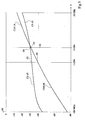
- Figure 3 shows the attenuation in dB at the level in box C1-15 and in box C14-14 of a signal sent by box C1-1, as a function of frequency (on a logarithmic scale) between 100 MHz and 10 GHz.
- box C1-15 we see that this attenuation decreases when the frequency increases.
- box C14-14 (or in any other box located inside the protective structure 10) we see that, up to a frequency of the order of a gigahertz, the attenuation is clearly more important than for box C1-15.
- the slope of the curve C14-14 changes and the attenuation provided by the isolation wall 15 becomes negligible.
- the isolation wall has a negative effect, at know that the attenuation of the signal from box C1-1 is less important in box C14-14 "protected" by the isolation structure 10 only in box C1-15 which is not not protected.
- an object of the present invention is to provide a new pest protection structure of a area of an integrated circuit formed on a solid substrate.
- the present invention provides a protective structure for a first zone of a semiconductor wafer comprising a lightly doped substrate of a first type of conductivity against high parasites frequency likely to be injected from components formed in the upper part of a second area of the edge, comprising a very heavily doped wall of the first type of conductivity having substantially the depth of said upper part, characterized in that said wall is divided into segments each of which is connected to a ground plane.
- the first type of conductivity is type P.
- the impedance between two successive segments is greater than the ground connection impedance of each segment.
- each segment is connected to a ground plane via a flip chip mounting.
- the isolation wall is surrounded by a moderately doped area of the first type of conductivity.
- the isolation wall according to the present invention is divided into segments 21 heavily doped with type P (P + ).
- a metallization 22 comes into contact with each segment and each of the metallizations 22 is independently connected to a ground plane.
- this connection is made by a flip chip type assembly as described above.
- each region 21 formed in a lightly doped P-type substrate 11 (P - ) is in contact with a metallization 22 itself surmounted by a solder ball 23 intended to ensure the flip chip mounting.
- P - lightly doped P-type substrate 11
- solder ball 23 intended to ensure the flip chip mounting.
- this representation is extremely schematic and we know in the art various means of preparing connections for a flip chip assembly.
- An insulating layer 24 has been shown on the surface of the semiconductor wafer which is open at the locations where the metallization 22 comes into contact with the segments 21.
- the depth of the isolation wall 21 will be that of a heavily doped P-type region (P + ) in the technology considered. Its width will preferably be less than the largest width of a contact pad 22.
- the upper part of the substrate 11 at vicinity of the isolation wall region 21 is constituted of a P-type doped region at a doping level intermediate between the doping of the substrate 11 and the very doping high of region 21.
- This region 25 can for example extend over a distance greater than 100 ⁇ m apart and on the other side of the isolation wall 21.
- the difference between the segments 21 and the doping of the region 25 of type P are chosen so that the impedance between two segments is greater than or equal to the contact impedance between region 21 and the ground plane to which it is connected by through metallization 22 and the solder ball 23.
Landscapes
- Semiconductor Integrated Circuits (AREA)
Abstract
Description
Claims (4)
- Structure de protection d'une première zone d'une tranche semiconductrice comprenant un substrat (11) faiblement dopé d'un premier type de conductivité contre des parasites haute fréquence susceptibles d'être injectés à partir de composants formés dans la partie supérieure d'une deuxième zone de la tranche, comprenant un mur (21) très fortement dopé du premier type de conductivité ayant sensiblement la profondeur de ladite partie supérieure, caractérisée en ce que ledit mur est divisé en segments dont chacun est connecté à un plan de masse par l'intermédiaire d'un montage de type flip chip.
- Structure de protection selon la revendication 1, caractérisée en ce que le premier type de conductivité est le type P.
- Structure de protection selon la revendication 1, caractérisée en ce que l'impédance entre deux segments successifs est supérieure à l'impédance de connexion à la masse de chaque segment.
- Structure de protection selon la revendication 1, caractérisée en ce que le mur d'isolement est entouré d'une zone (25) moyennement dopée du premier type de conductivité.
Applications Claiming Priority (2)
| Application Number | Priority Date | Filing Date | Title |
|---|---|---|---|
| FR0101525A FR2820547A1 (fr) | 2001-02-05 | 2001-02-05 | Structure de protection contre des parasites |
| FR0101525 | 2001-02-05 |
Publications (2)
| Publication Number | Publication Date |
|---|---|
| EP1229587A1 true EP1229587A1 (fr) | 2002-08-07 |
| EP1229587B1 EP1229587B1 (fr) | 2004-08-11 |
Family
ID=8859625
Family Applications (1)
| Application Number | Title | Priority Date | Filing Date |
|---|---|---|---|
| EP02354022A Expired - Lifetime EP1229587B1 (fr) | 2001-02-05 | 2002-02-04 | Structure de protection contre des parasites |
Country Status (4)
| Country | Link |
|---|---|
| US (1) | US6762462B2 (fr) |
| EP (1) | EP1229587B1 (fr) |
| DE (1) | DE60200894T2 (fr) |
| FR (1) | FR2820547A1 (fr) |
Families Citing this family (1)
| Publication number | Priority date | Publication date | Assignee | Title |
|---|---|---|---|---|
| FR2820546B1 (fr) * | 2001-02-05 | 2003-07-11 | St Microelectronics Sa | Structure de protection contre des parasites |
Citations (3)
| Publication number | Priority date | Publication date | Assignee | Title |
|---|---|---|---|---|
| EP0081396A2 (fr) * | 1981-12-04 | 1983-06-15 | National Aeronautics And Space Administration | Transistor à effet de champ à hyperfréquences |
| US5821148A (en) * | 1995-06-07 | 1998-10-13 | Vtc Inc. | Method of fabricating a segmented emitter low noise transistor |
| FR2787636A1 (fr) * | 1998-12-17 | 2000-06-23 | St Microelectronics Sa | Dispositif semi-conducteur avec substrat du type bicmos a decouplage de bruit |
Family Cites Families (2)
| Publication number | Priority date | Publication date | Assignee | Title |
|---|---|---|---|---|
| JP3131823B2 (ja) * | 1996-05-16 | 2001-02-05 | 株式会社サンコーシヤ | 多端子サージ防護デバイス |
| SE518231C2 (sv) * | 2000-05-12 | 2002-09-10 | Ericsson Telefon Ab L M | Förfarande för brusfördelning i substrat med hög resistivitet som innefattar differentiell eller balanserad integrerad koppling |
-
2001
- 2001-02-05 FR FR0101525A patent/FR2820547A1/fr active Pending
-
2002
- 2002-02-04 DE DE60200894T patent/DE60200894T2/de not_active Expired - Fee Related
- 2002-02-04 EP EP02354022A patent/EP1229587B1/fr not_active Expired - Lifetime
- 2002-02-05 US US10/068,308 patent/US6762462B2/en not_active Expired - Fee Related
Patent Citations (3)
| Publication number | Priority date | Publication date | Assignee | Title |
|---|---|---|---|---|
| EP0081396A2 (fr) * | 1981-12-04 | 1983-06-15 | National Aeronautics And Space Administration | Transistor à effet de champ à hyperfréquences |
| US5821148A (en) * | 1995-06-07 | 1998-10-13 | Vtc Inc. | Method of fabricating a segmented emitter low noise transistor |
| FR2787636A1 (fr) * | 1998-12-17 | 2000-06-23 | St Microelectronics Sa | Dispositif semi-conducteur avec substrat du type bicmos a decouplage de bruit |
Also Published As
| Publication number | Publication date |
|---|---|
| EP1229587B1 (fr) | 2004-08-11 |
| US20020121649A1 (en) | 2002-09-05 |
| DE60200894T2 (de) | 2005-09-01 |
| FR2820547A1 (fr) | 2002-08-09 |
| DE60200894D1 (de) | 2004-09-16 |
| US6762462B2 (en) | 2004-07-13 |
Similar Documents
| Publication | Publication Date | Title |
|---|---|---|
| US6538299B1 (en) | Silicon-on-insulator (SOI) trench photodiode | |
| US4847210A (en) | Integrated pin photo-detector method | |
| US4926231A (en) | Integrated pin photo-detector | |
| FR2812972A1 (fr) | Dispositif a semiconducteur consistant en un thyristor pour la protection contre les decharges electrostatiques | |
| EP0963608A1 (fr) | Circuit de protection d'interface d'abonnes | |
| EP0490787B1 (fr) | Circuit de protection limitant les surtensions entre limites choisies et son intégration monolithique | |
| EP1187206A1 (fr) | Dispositif intégré de protection électromagnétique | |
| EP1011143B1 (fr) | Dispositif semi-conducteur avec substrat du type BiCMOS à découplage de bruit | |
| EP1229587B1 (fr) | Structure de protection contre des parasites | |
| FR2684804A1 (fr) | Dispositif de montage de circuits integres monolithiques hyperfrequences a tres large bande. | |
| EP3696865B1 (fr) | Photodiode | |
| EP1521363B1 (fr) | Coupleur intégré | |
| EP1371097B1 (fr) | Structure de protection contre des parasites | |
| US6313484B1 (en) | Circuit-integrated light-receiving device | |
| FR2770341A1 (fr) | Dispositif de protection contre des decharges electrostatiques a faible niveau de seuil | |
| FR3131981A1 (fr) | Dispositif de protection contre les décharges électrostatiques | |
| US20030137026A1 (en) | Avalanche photodiode having an electrically isolated deep guard ring | |
| EP1553812A2 (fr) | Puce à semiconducteur et circuit comprenant une inductance blindée | |
| FR2596202A1 (fr) | Structure de transistor npn equivalent a tension de claquage plus elevee que la tension de claquage intrinseque des transistors npn | |
| FR3011121A1 (fr) | Assemblage de puces de circuits integres comprenant un composant de protection contre les surtensions | |
| EP4287263A1 (fr) | Transistor bipolaire latéral | |
| EP0872893A1 (fr) | Transistor PNP latéral dans une technologie BICMOS | |
| FR3103320A1 (fr) | Circuit intégré comprenant un transistor jfet et procédé de fabrication d’un tel circuit intégré | |
| FR2561822A1 (fr) | Dispositif semi-conducteur a effet de champ a faible tension de dechet | |
| FR2818013A1 (fr) | Transistor a effet de champ a jonction destine a former un limiteur de courant |
Legal Events
| Date | Code | Title | Description |
|---|---|---|---|
| PUAI | Public reference made under article 153(3) epc to a published international application that has entered the european phase |
Free format text: ORIGINAL CODE: 0009012 |
|
| AK | Designated contracting states |
Kind code of ref document: A1 Designated state(s): AT BE CH CY DE DK ES FI FR GB GR IE IT LI LU MC NL PT SE TR |
|
| AX | Request for extension of the european patent |
Free format text: AL;LT;LV;MK;RO;SI |
|
| RIN1 | Information on inventor provided before grant (corrected) |
Inventor name: BELOT, DIDIER |
|
| 17P | Request for examination filed |
Effective date: 20030117 |
|
| AKX | Designation fees paid |
Designated state(s): DE FR GB IT |
|
| 17Q | First examination report despatched |
Effective date: 20030623 |
|
| GRAP | Despatch of communication of intention to grant a patent |
Free format text: ORIGINAL CODE: EPIDOSNIGR1 |
|
| GRAS | Grant fee paid |
Free format text: ORIGINAL CODE: EPIDOSNIGR3 |
|
| GRAA | (expected) grant |
Free format text: ORIGINAL CODE: 0009210 |
|
| AK | Designated contracting states |
Kind code of ref document: B1 Designated state(s): DE FR GB IT |
|
| REG | Reference to a national code |
Ref country code: GB Ref legal event code: FG4D Free format text: NOT ENGLISH |
|
| GBT | Gb: translation of ep patent filed (gb section 77(6)(a)/1977) |
Effective date: 20040811 |
|
| REG | Reference to a national code |
Ref country code: IE Ref legal event code: FG4D Free format text: FRENCH |
|
| REF | Corresponds to: |
Ref document number: 60200894 Country of ref document: DE Date of ref document: 20040916 Kind code of ref document: P |
|
| REG | Reference to a national code |
Ref country code: IE Ref legal event code: FD4D |
|
| PLBE | No opposition filed within time limit |
Free format text: ORIGINAL CODE: 0009261 |
|
| STAA | Information on the status of an ep patent application or granted ep patent |
Free format text: STATUS: NO OPPOSITION FILED WITHIN TIME LIMIT |
|
| 26N | No opposition filed |
Effective date: 20050512 |
|
| PGFP | Annual fee paid to national office [announced via postgrant information from national office to epo] |
Ref country code: GB Payment date: 20060201 Year of fee payment: 5 |
|
| PGFP | Annual fee paid to national office [announced via postgrant information from national office to epo] |
Ref country code: DE Payment date: 20060202 Year of fee payment: 5 |
|
| PGFP | Annual fee paid to national office [announced via postgrant information from national office to epo] |
Ref country code: FR Payment date: 20060220 Year of fee payment: 5 |
|
| PGFP | Annual fee paid to national office [announced via postgrant information from national office to epo] |
Ref country code: IT Payment date: 20060228 Year of fee payment: 5 |
|
| GBPC | Gb: european patent ceased through non-payment of renewal fee |
Effective date: 20070204 |
|
| REG | Reference to a national code |
Ref country code: FR Ref legal event code: ST Effective date: 20071030 |
|
| PG25 | Lapsed in a contracting state [announced via postgrant information from national office to epo] |
Ref country code: DE Free format text: LAPSE BECAUSE OF NON-PAYMENT OF DUE FEES Effective date: 20070901 |
|
| PG25 | Lapsed in a contracting state [announced via postgrant information from national office to epo] |
Ref country code: FR Free format text: LAPSE BECAUSE OF NON-PAYMENT OF DUE FEES Effective date: 20070228 Ref country code: GB Free format text: LAPSE BECAUSE OF NON-PAYMENT OF DUE FEES Effective date: 20070204 |
|
| PG25 | Lapsed in a contracting state [announced via postgrant information from national office to epo] |
Ref country code: IT Free format text: LAPSE BECAUSE OF NON-PAYMENT OF DUE FEES Effective date: 20070204 |