EP1229362A2 - Planar light waveguide circuit with landmarks - Google Patents
Planar light waveguide circuit with landmarks Download PDFInfo
- Publication number
- EP1229362A2 EP1229362A2 EP01126046A EP01126046A EP1229362A2 EP 1229362 A2 EP1229362 A2 EP 1229362A2 EP 01126046 A EP01126046 A EP 01126046A EP 01126046 A EP01126046 A EP 01126046A EP 1229362 A2 EP1229362 A2 EP 1229362A2
- Authority
- EP
- European Patent Office
- Prior art keywords
- light waveguide
- planar light
- landmarks
- waveguide circuit
- circuit
- Prior art date
- Legal status (The legal status is an assumption and is not a legal conclusion. Google has not performed a legal analysis and makes no representation as to the accuracy of the status listed.)
- Withdrawn
Links
Images




Classifications
-
- G—PHYSICS
- G02—OPTICS
- G02B—OPTICAL ELEMENTS, SYSTEMS OR APPARATUS
- G02B6/00—Light guides; Structural details of arrangements comprising light guides and other optical elements, e.g. couplings
- G02B6/10—Light guides; Structural details of arrangements comprising light guides and other optical elements, e.g. couplings of the optical waveguide type
- G02B6/12—Light guides; Structural details of arrangements comprising light guides and other optical elements, e.g. couplings of the optical waveguide type of the integrated circuit kind
- G02B6/122—Basic optical elements, e.g. light-guiding paths
-
- G—PHYSICS
- G02—OPTICS
- G02B—OPTICAL ELEMENTS, SYSTEMS OR APPARATUS
- G02B6/00—Light guides; Structural details of arrangements comprising light guides and other optical elements, e.g. couplings
- G02B6/10—Light guides; Structural details of arrangements comprising light guides and other optical elements, e.g. couplings of the optical waveguide type
- G02B6/12—Light guides; Structural details of arrangements comprising light guides and other optical elements, e.g. couplings of the optical waveguide type of the integrated circuit kind
-
- G—PHYSICS
- G02—OPTICS
- G02B—OPTICAL ELEMENTS, SYSTEMS OR APPARATUS
- G02B6/00—Light guides; Structural details of arrangements comprising light guides and other optical elements, e.g. couplings
- G02B6/24—Coupling light guides
- G02B6/26—Optical coupling means
- G02B6/30—Optical coupling means for use between fibre and thin-film device
Definitions
- the present invention relates generally to a planar light waveguide circuit, and in particular, to a planar light waveguide circuit with landmarks and a method of manufacturing the same.
- a general light waveguide component is equivalent to a light transmission line for propagating optical waves with a small loss by confining the optical waves within the waveguide component in a longitudinal direction.
- the light waveguide could be formed in a substrate with a high refractive index and a cladding with a low refractive index, where the cladding is surrounded by the core.
- a process for packaging the conventional planar light waveguide circuit will be described below with reference to FIGs. 1 and 2.
- a conventional planar light waveguide circuit (PLC) 10 is packaged in way that the PLC 10 is in alignment with optical fiber blocks 11 and 12, which are used for receiving and outputting a light beam from or to the PLC 10.
- the PLC 10 is manufactured by depositing a multi-layer silica or polymer film in a silicon or quartz substrate for dividing the light strength and wavelength, changing the light path, and adjusting the light strength using a refractive index difference between the core and the cladding surrounding the core.
- the optical fiber blocks 11 and 12 serve to support optical fibers 13 and 14, respectively, and are manufactured by forming a V-groove on the silicon substrate.
- the optical fiber blocks 11 and 12 arrange the optical fiber 13 and the ribbon-type optical fiber 14 in the V-groove, thus fixing them to the planar light waveguide circuit 10.
- the PLC 10 is aligned with the optical fiber blocks 11 and 12, located at both ends thereof, through a precise position control device and then fixed (or glued) to the aligned optical fiber blocks 11 and 12 by applying the glue 17 to the contact areas.
- an ultraviolet or thermo-setting glue is typically used for the glue 17.
- the PLC 10 can be also fixed to the optical fiber blocks 11 and 12 through a welding operation instead of using the glue 17.
- the PLC 10 is packaged in a metal or plastic housing 15, and furthermore, the PLC 10 may be subject to a hermetic sealing as occasion demands.
- an external power connector is connected to the housing 15 to provide a current to the light waveguide circuit.
- reference numeral 16 denotes a power lead.
- the section cutting process includes a combination of the cutting technique using a blade and the polishing technique using abrasives.
- An accuracy of the section cutting process is closely related to a coupling loss, which occurs at the junction where the light waveguide circuit is coupled to the optical fiber blocks.
- the sloped cut section typically causes a decrease in the uniformity of an insertion loss. Therefore, a separate process for measuring the accuracy of the section cutting process is required in the prior art. If the cutting process is inaccurate, the process must be repeated and sometimes, if excessively cut, the light waveguide circuit must be discarded.
- the present invention relates to a planar light waveguide circuit capable of minimizing a coupling loss, which occurs when the planar light waveguide circuit is being coupled to the optical fiber blocks, by accurately measuring the slope of a cut section of the planar light waveguide circuit and correcting the slope end of the optical fiber blocks.
- the present invention provides a planar light waveguide circuit with landmarks used for aligning the planar waveguide circuit to the optical fiber block components.
- the present invention relates to a planar light waveguide circuit, which includes a plurality of landmarks arranged along one end of the planar light waveguide circuit at intervals of a predetermined gap so as to increase the uniformity of a coupling loss occurring when connecting the planar light waveguide circuit in alignment with the optical fiber blocks.
- the landmarks are formed onto the planar light waveguide circuit so as to enable an operator to monitor a permissible angle error when cutting the side of the planar light waveguide circuit.
- Arabic numerals or specific symbols are noted in association with the landmarks indicated on the planar light waveguide circuit to assist the operator distinguish relative position of the landmarks during the cutting process.
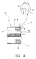
- FIG. 3 illustrates a planar light waveguide circuit 30 with an array of landmarks 32 according to an exemplary embodiment of the present invention.
- the landmarks 32 are provided on both ends of the planar light waveguide circuit 30 prior to cutting the section 30a, such that a segment AB should be perpendicular to a light waveguide 31. That is, the section 30a defining the boundary of the planar light waveguide circuit 30 at both ends should be cut at a right angle to the light waveguide 31.
- an angle ⁇ is variable. Therefore, it is also possible to cut section 30a at a non-right angle to the light waveguide 31.
- a sufficient number of the landmarks 32 are formed starting from the cut section 30a at intervals of the gap "t", and the Arabic numerals or specific symbols are marked next to each of the landmarks 32 in order to identify the position of each landmark 32.
- the landmarks 32 are formed on the planar light waveguide circuit 30 by depositing a film on a silicon or quartz substrate, applying a photomask with a specific pattern onto the film, then etching the photomask. Therefore, the accuracy of the angle between the landmarks 32 and the light waveguide 31 depends upon the accuracy of an electron beam cutting process.
- section 30a can be selectively cut and the amount of deviation relative to the landmark 32 can be minotored.
- the operator monitors how much the landmarks 32 are removed using a microscope.
- the operator can selectively adjust the angle of cutting the end of the planar light waveguide circuit 30 to a desired position by observing the area of the landmarks next to section 30a.
- the cut section 30a deviates, for example, from the segment AB' or AB
- the operator can cut section 30a again after correcting the angle. If the cut section 30a does not deviate from the segment AB' or AB" or falls within the acceptable error angle, the operator may terminate the cutting process.
- FIGs. 4A to 5B are plane views illustrating states where the planar light waveguide circuit is connected in alignment with the optical fiber blocks according to an embodiment of the present invention.
- an optical fiber block 41 with a single optical fiber 43 and an optical fiber block 42 with a group of optical fibers 44 are connected in alignment with both cut sections 40a and 40b of the planar light waveguide circuit 40, respectively.
- the planar light waveguide circuit 40 is fixed to the optical fiber blocks 41 and 42 using an ultraviolet or thermo-setting glue 45.
- a silicon or quartz substrate can be used for the optical fiber blocks 41 and 42.
- an optical fiber block 51 with a single optical fiber 53 and an optical fiber block 52 with a group of optical fibers 54 are connected in alignment with a cut section 50a of a planar light waveguide circuit 50.
- the planar light waveguide circuit 50 is fixed to the optical fiber blocks 51 and 52 using an ultraviolet or thermo-setting glue 55.
- a silicon or quartz substrate can be used for the optical fiber blocks 51 and 52.
- the optical fiber blocks 41 and 42 can be connected in alignment with the planar light waveguide circuit 40 at its both ends as shown in FIGs. 4A and 4B.
- the optical fiber blocks 51 and 52 can be connected in alignment with the planar light waveguide circuit 50 at its one end as shown in FIGs. 5A and 5B.
- FIGs. 4A and 5A illustrate states where the optical fiber blocks are aligned with the planar light waveguide circuit
- FIGs. 4B and 5B illustrate states where the optical fiber blocks are fixed to the planar light waveguide circuit using the glue.
- the operator can easily monitor the cutting state through the microscope, thereby making it possible to match the sections of the optical fiber blocks with the associated cut sections of the planar light waveguide circuit. That is, it is possible to maximize the uniformity of the coupling loss by matching a positive angle error of the planar light waveguide circuit with a positive angle error of the optical fiber blocks, and matching a negative angle error of the planar light waveguide circuit with a negative angle error of the optical fiber blocks.
- an array of landmarks may be provided on the optical block so that a desired matching angle can be precisely cut along the matching end of the optical block.
- FIG. 6 illustrates a state where the cut sections 60a and 60b of the planar light waveguide circuit 60 are perpendicular to the optical fiber blocks 61 and 62, respectively
- FIG. 7 illustrates a state where the cut sections 70a and 70b of the planar light waveguide circuit 70 are sloped at an angle of 8° or 12° with respect to the optical fiber blocks 71 and 72, respectively.
- the cut sections 60a and 60b of the planar light waveguide circuit 60 are aligned (or matched) with the cut sections 61a and 62a of the optical fiber blocks 61 and 62, respectively, on a face-to-face basis.
- the cut sections 70a and 70b of the planar light waveguide circuit 70 are aligned with the cut sections 71a and 72a of the optical fiber blocks 71 and 72, respectively, on a face-to-face basis.
- the novel planar light waveguide circuit has a plurality of landmarks formed on its surface, thus making it possible to increase the accuracy of the cutting process and the yield of the elements.
- the landmarks according to the present invention could be applied to optical elements such as an optical power divider, a wavelength divider, a switch, an attenuator, an ADM (Add Drop Multiplexing) apparatus, an OADM (Optical Add Drop Multiplexing) apparatus, and a TADM apparatus.
- optical elements such as an optical power divider, a wavelength divider, a switch, an attenuator, an ADM (Add Drop Multiplexing) apparatus, an OADM (Optical Add Drop Multiplexing) apparatus, and a TADM apparatus.
Landscapes
- Physics & Mathematics (AREA)
- General Physics & Mathematics (AREA)
- Optics & Photonics (AREA)
- Engineering & Computer Science (AREA)
- Microelectronics & Electronic Packaging (AREA)
- Optical Couplings Of Light Guides (AREA)
- Optical Integrated Circuits (AREA)
- Mechanical Coupling Of Light Guides (AREA)
Abstract
Description
Claims (10)
- A planar light waveguide circuit comprising:wherein the plurality of said landmarks is operative for selectively cutting one side of the planar light waveguide within a permissible angle error.a planar light waveguide including a core and a cladding;a plurality of landmarks arranged at opposite ends within the planar light waveguide, each landmark being spaced apart from an adjacent landmark at a predetermined interval (t) starting at one end of the planar light waveguide;
- The circuit as claimed in claim 1, wherein the predetermined interval (t) between adjacent landmarks is defined as:
- The circuit as claimed in claim 1 or 2, wherein the landmarks are formed onto the planar light waveguide circuit so as to enable an operator to monitor the permissible angle error.
- The circuit as claimed in one of the claims 1 to 3, wherein the planar light waveguide circuit includes an optical power divider, a wavelength divider, a switch, an attenuator, an ADM (Add Drop Multiplexing) apparatus, an OADM (Optical Add Drop Multiplexing) apparatus, and a TADM apparatus.
- The circuit as claimed in one of the claims 1 to 4, wherein Arabic numerals or specific symbols are marked in association with the landmarks to distinguish the landmarks.
- A method for aligning a planar light waveguide circuit having a plurality of waveguides to an optical block, comprising the steps of:cutting said planar light waveguide circuit to provide a cut section that is perpendicular to the plurality of said waveguides;providing an array of landmarks, each landmark being spaced apart from an adjacent landmark at a predetermined interval (t) starting at one end of said cut section and at the other end of said cut section, said one end of said landmarks is synchronized, in sequence, with said other end of said landmarks;identifying a sequence order of each of said landmarks according to predetermined criteria; and,selectively cutting one side of said planar light waveguide circuit to cover the first landmark of said one end of said planar light waveguide circuit and the first landmark of said other end of said planar light waveguide circuit within a permissible angle error.
- The method of claim 6, further comprising the step of monitoring said permissible angle error to provide the corresponding receiving end section of said optical fiber block, said landmarks being formed onto said planar light waveguide circuit so as to enable an operator to monitor said permissible angle error.
- The method of claim 6 or 7, wherein said predetermined interval (t) between adjacent landmarks is defined as:
- The method of one of the claims 6 to 8, wherein said planar light waveguide circuit includes an optical power divider, a wavelength divider, a switch, an attenuator, an ADM (Add Drop Multiplexing) apparatus, an OADM (Optical Add Drop Multiplexing) apparatus, and a TADM apparatus.
- The method of one of the claims 6 to 9, wherein said predetermined criteria includes Arabic numerals or specific symbols to distinguish said landmarks.
Applications Claiming Priority (2)
| Application Number | Priority Date | Filing Date | Title |
|---|---|---|---|
| KR2000087199 | 2000-12-30 | ||
| KR1020000087199A KR100357853B1 (en) | 2000-12-30 | 2000-12-30 | Plannar light waveguide circuit element using landmark |
Publications (2)
| Publication Number | Publication Date |
|---|---|
| EP1229362A2 true EP1229362A2 (en) | 2002-08-07 |
| EP1229362A3 EP1229362A3 (en) | 2004-06-16 |
Family
ID=19704109
Family Applications (1)
| Application Number | Title | Priority Date | Filing Date |
|---|---|---|---|
| EP01126046A Withdrawn EP1229362A3 (en) | 2000-12-30 | 2001-10-31 | Planar light waveguide circuit with landmarks |
Country Status (4)
| Country | Link |
|---|---|
| US (1) | US6574410B2 (en) |
| EP (1) | EP1229362A3 (en) |
| JP (1) | JP3501789B2 (en) |
| KR (1) | KR100357853B1 (en) |
Families Citing this family (9)
| Publication number | Priority date | Publication date | Assignee | Title |
|---|---|---|---|---|
| KR20030000285A (en) * | 2001-06-23 | 2003-01-06 | 삼성전자 주식회사 | Wavelength division multiplexer using planar lightwave circuit |
| US20040145381A1 (en) * | 2001-12-28 | 2004-07-29 | Jun Su | Test fixture for die-level testing of planar lightwave circuits |
| JP4116420B2 (en) * | 2002-12-18 | 2008-07-09 | 富士通株式会社 | Electrical contact device and method of manufacturing the same |
| JP4144427B2 (en) * | 2003-05-12 | 2008-09-03 | オムロン株式会社 | Optical waveguide and method for manufacturing the same |
| JP2006133666A (en) * | 2004-11-09 | 2006-05-25 | Mitsumi Electric Co Ltd | Optical transmission module and manufacturing method thereof |
| JP2006322999A (en) * | 2005-05-17 | 2006-11-30 | Matsushita Electric Works Ltd | Optical waveguide module |
| JP2009270844A (en) * | 2008-04-30 | 2009-11-19 | Panasonic Electric Works Co Ltd | Live line detection device for optical fiber |
| US20130335110A1 (en) * | 2012-06-15 | 2013-12-19 | Polyvalor, Limited Partnership | Planar circuit test fixture |
| WO2017047076A1 (en) * | 2015-09-18 | 2017-03-23 | 日本電気株式会社 | Optical waveguide element |
Family Cites Families (8)
| Publication number | Priority date | Publication date | Assignee | Title |
|---|---|---|---|---|
| JPH0769497B2 (en) * | 1988-02-05 | 1995-07-31 | 日本電信電話株式会社 | Optical component mount |
| JPH0411204A (en) * | 1990-04-27 | 1992-01-16 | Furukawa Electric Co Ltd:The | Buried optical waveguide |
| JP3054278B2 (en) * | 1992-11-16 | 2000-06-19 | 日本碍子株式会社 | Manufacturing method of optical integrated circuit |
| US5359686A (en) * | 1993-03-29 | 1994-10-25 | Motorola, Inc. | Interface for coupling optical fibers to electronic circuitry |
| US5555333A (en) * | 1993-07-12 | 1996-09-10 | Ricoh Company, Ltd. | Optical module and a fabrication process thereof |
| JP3293115B2 (en) * | 1994-08-11 | 2002-06-17 | 住友電気工業株式会社 | Optical fiber array and optical waveguide module coupling method |
| JPH10256664A (en) * | 1997-03-13 | 1998-09-25 | Fujitsu Ltd | Marker forming method for optical semiconductor device |
| US6046101A (en) * | 1997-12-31 | 2000-04-04 | Intel Corporation | Passivation technology combining improved adhesion in passivation and a scribe street without passivation |
-
2000
- 2000-12-30 KR KR1020000087199A patent/KR100357853B1/en not_active Expired - Fee Related
-
2001
- 2001-09-28 US US09/967,006 patent/US6574410B2/en not_active Expired - Lifetime
- 2001-10-31 EP EP01126046A patent/EP1229362A3/en not_active Withdrawn
- 2001-12-11 JP JP2001377846A patent/JP3501789B2/en not_active Expired - Fee Related
Also Published As
| Publication number | Publication date |
|---|---|
| KR100357853B1 (en) | 2002-10-25 |
| JP2002214468A (en) | 2002-07-31 |
| EP1229362A3 (en) | 2004-06-16 |
| US20020118940A1 (en) | 2002-08-29 |
| JP3501789B2 (en) | 2004-03-02 |
| KR20020056975A (en) | 2002-07-11 |
| US6574410B2 (en) | 2003-06-03 |
Similar Documents
| Publication | Publication Date | Title |
|---|---|---|
| KR100928408B1 (en) | Optical circuit manufacturing method and device | |
| KR100389837B1 (en) | Packaging device for waveguide element | |
| JP6798996B2 (en) | Multiport optical probe for characterization and packaging of optical integrated circuits | |
| US6647184B2 (en) | Optical waveguide device and method of manufacturing the same | |
| EP1561139B1 (en) | Optical component for free-space optical propagation between waveguides | |
| KR100360766B1 (en) | Arrayed waveguide grating type optical multiplexer/demultiplexer and a method of manufacturing the same | |
| EP1743201B1 (en) | Athermal awg and awg with low power consumption using groove of changeable width | |
| KR19980030121A (en) | Optical module with lens aligned in V-groove and manufacturing method thereof | |
| US6788848B2 (en) | Arrayed waveguide grating device, process for producing the same, arrayed waveguide module, and optical communication system | |
| US7218806B2 (en) | Multi-wavelength optical transceiver module, and multiplexer/demultiplexer using thin film filter | |
| EP1229362A2 (en) | Planar light waveguide circuit with landmarks | |
| JP2003240992A (en) | Waveguide element and waveguide device | |
| KR101501140B1 (en) | Planar Lightwave Circuit Module Having an Improved Structure of an Optical Power Monitor | |
| KR100681787B1 (en) | Optical waveguide chip and optical fiber array block for passive alignment and manual alignment method between them | |
| JP2002131566A (en) | Optical component, optical circuit, and optical circuit manufacturing method having optical waveguide interval conversion unit | |
| EP1688768A1 (en) | Optical multiplexer/demultiplexer and manufacturing method thereof | |
| JP3549404B2 (en) | Method of manufacturing filter-inserted waveguide device | |
| JPH10133069A (en) | Optical transceiver module | |
| JPH1138240A (en) | Optical waveguide and its manufacturing method | |
| JP4792422B2 (en) | Planar lightwave circuit | |
| JPH11183750A (en) | Manufacture of optical waveguide module for optical device, and optical device | |
| JP2000241637A (en) | Manufacturing method of optical wavelength multiplexer / demultiplexer | |
| JPH063555A (en) | Optical branching device | |
| KR20040067276A (en) | Athermal wavelength division multiplexer/demultiplexer with aligning improvement and aligning method thereof | |
| JPH11295540A (en) | 2-wavelength optical multiplexer / demultiplexer |
Legal Events
| Date | Code | Title | Description |
|---|---|---|---|
| PUAI | Public reference made under article 153(3) epc to a published international application that has entered the european phase |
Free format text: ORIGINAL CODE: 0009012 |
|
| 17P | Request for examination filed |
Effective date: 20011031 |
|
| AK | Designated contracting states |
Kind code of ref document: A2 Designated state(s): AT BE CH CY DE DK ES FI FR GB GR IE IT LI LU MC NL PT SE TR |
|
| AX | Request for extension of the european patent |
Free format text: AL;LT;LV;MK;RO;SI |
|
| PUAL | Search report despatched |
Free format text: ORIGINAL CODE: 0009013 |
|
| AK | Designated contracting states |
Kind code of ref document: A3 Designated state(s): AT BE CH CY DE DK ES FI FR GB GR IE IT LI LU MC NL PT SE TR |
|
| AX | Request for extension of the european patent |
Extension state: AL LT LV MK RO SI |
|
| AKX | Designation fees paid |
Designated state(s): DE FR GB |
|
| STAA | Information on the status of an ep patent application or granted ep patent |
Free format text: STATUS: THE APPLICATION IS DEEMED TO BE WITHDRAWN |
|
| 18D | Application deemed to be withdrawn |
Effective date: 20070501 |