EP1227581A2 - Bulk acoustic wave resonator with a conductive acoustic mirror - Google Patents
Bulk acoustic wave resonator with a conductive acoustic mirror Download PDFInfo
- Publication number
- EP1227581A2 EP1227581A2 EP02250263A EP02250263A EP1227581A2 EP 1227581 A2 EP1227581 A2 EP 1227581A2 EP 02250263 A EP02250263 A EP 02250263A EP 02250263 A EP02250263 A EP 02250263A EP 1227581 A2 EP1227581 A2 EP 1227581A2
- Authority
- EP
- European Patent Office
- Prior art keywords
- resonator
- isolation structure
- substrate
- mirror
- baw
- Prior art date
- Legal status (The legal status is an assumption and is not a legal conclusion. Google has not performed a legal analysis and makes no representation as to the accuracy of the status listed.)
- Granted
Links
Images




Classifications
-
- H—ELECTRICITY
- H03—ELECTRONIC CIRCUITRY
- H03H—IMPEDANCE NETWORKS, e.g. RESONANT CIRCUITS; RESONATORS
- H03H9/00—Networks comprising electromechanical or electro-acoustic elements; Electromechanical resonators
- H03H9/02—Details
- H03H9/05—Holders or supports
- H03H9/10—Mounting in enclosures
- H03H9/1007—Mounting in enclosures for bulk acoustic wave [BAW] devices
- H03H9/105—Mounting in enclosures for bulk acoustic wave [BAW] devices the enclosure being defined by a cover cap mounted on an element forming part of the BAW device
-
- H—ELECTRICITY
- H03—ELECTRONIC CIRCUITRY
- H03H—IMPEDANCE NETWORKS, e.g. RESONANT CIRCUITS; RESONATORS
- H03H3/00—Apparatus or processes specially adapted for the manufacture of impedance networks, resonating circuits, resonators
- H03H3/007—Apparatus or processes specially adapted for the manufacture of impedance networks, resonating circuits, resonators for the manufacture of electromechanical resonators or networks
- H03H3/02—Apparatus or processes specially adapted for the manufacture of impedance networks, resonating circuits, resonators for the manufacture of electromechanical resonators or networks for the manufacture of piezoelectric or electrostrictive resonators or networks
-
- H—ELECTRICITY
- H03—ELECTRONIC CIRCUITRY
- H03H—IMPEDANCE NETWORKS, e.g. RESONANT CIRCUITS; RESONATORS
- H03H9/00—Networks comprising electromechanical or electro-acoustic elements; Electromechanical resonators
- H03H9/15—Constructional features of resonators consisting of piezoelectric or electrostrictive material
- H03H9/17—Constructional features of resonators consisting of piezoelectric or electrostrictive material having a single resonator
- H03H9/171—Constructional features of resonators consisting of piezoelectric or electrostrictive material having a single resonator implemented with thin-film techniques, i.e. of the film bulk acoustic resonator [FBAR] type
- H03H9/172—Means for mounting on a substrate, i.e. means constituting the material interface confining the waves to a volume
- H03H9/175—Acoustic mirrors
-
- H—ELECTRICITY
- H10—SEMICONDUCTOR DEVICES; ELECTRIC SOLID-STATE DEVICES NOT OTHERWISE PROVIDED FOR
- H10W—GENERIC PACKAGES, INTERCONNECTIONS, CONNECTORS OR OTHER CONSTRUCTIONAL DETAILS OF DEVICES COVERED BY CLASS H10
- H10W72/00—Interconnections or connectors in packages
- H10W72/851—Dispositions of multiple connectors or interconnections
- H10W72/874—On different surfaces
- H10W72/884—Die-attach connectors and bond wires
-
- Y—GENERAL TAGGING OF NEW TECHNOLOGICAL DEVELOPMENTS; GENERAL TAGGING OF CROSS-SECTIONAL TECHNOLOGIES SPANNING OVER SEVERAL SECTIONS OF THE IPC; TECHNICAL SUBJECTS COVERED BY FORMER USPC CROSS-REFERENCE ART COLLECTIONS [XRACs] AND DIGESTS
- Y10—TECHNICAL SUBJECTS COVERED BY FORMER USPC
- Y10T—TECHNICAL SUBJECTS COVERED BY FORMER US CLASSIFICATION
- Y10T29/00—Metal working
- Y10T29/42—Piezoelectric device making
Definitions
- the present invention relates to bulk acoustic wave resonators, such as are used in providing bulk acoustic wave filters. More particularly, the present invention relates to bulk acoustic wave resonators with a particular variety of acoustic mirror, one including only metallic layers.
- a thin film bulk acoustical wave (BAW) filter can be fabricated on various substrates, such as silicon (Si), gallium arsenide (GaAs), or silicon dioxide (SiO2).
- a thin film BAW filter often includes a shunt BAW resonator and a series BAW resonator, although some filters include only a series resonator and a shunt capacitor or only a shunt resonator and a series capacitor, and other resonator are based on topologies such as the lattice filter topology.
- a BAW filter including a series resonator and a shunt resonator could also include several such pairs of resonators so as to form what is called a ladder filter.
- Each BAW resonator includes a top electrode deposited atop a layer of piezoelectric material, which in turn sits atop a bottom electrode.
- the assembly of these three layers is sometimes referred to as the resonator section of a BAW resonator.
- a BAW resonator further includes other layers of materials, or different structural arrangements of materials, so as to fine-tune the performance of the BAW resonator.
- BAW resonators Two types of BAW resonators are known in the art: a bridge type BAW resonator and an acoustic mirror type BAW resonator.
- a bridge type BAW resonator the resonator section is deposited on a membrane (made from one or more layers of different materials) and acoustic waves generated by the resonator are reflected back from the air interface above the top electrode, and below the membrane on which the resonator section is deposited.
- a mirror type of BAW resonator the resonator is solidly mounted on top of a stack of layers making up what is called an acoustic mirror.
- the layers are selected to present to acoustic waves created by the resonator section alternately high and low acoustic impedance.
- Each layer of material in an acoustic mirror is typically one quarter of a wavelength thick.
- Such an acoustic mirror provides for a large reflection factor back toward the resonator for acoustic waves created by the resonator propagating in the direction of the acoustic mirror. There is also a reflection of the acoustic waves created by the resonator at the air interface at the top electrode.
- BAW resonators Both types of BAW resonators have the disadvantage that they require a protective package with an air cavity over the resonator section.
- the packages typically used are similar to those used for SAW-filters, i.e. hermetic or at least semi-hermetic sealed ceramic packages. Such packages increase the size of the components and also the price. In addition, such packages create parasitic inductances and resistances.
- the present invention provides a method of fabricating a bulk acoustic wave (BAW) resonator and a BAW resonator so fabricated, the method including the steps of: providing a substrate; providing a first isolation structure; and providing a resonator section, the resonator section comprising a piezolayer; wherein the first isolation structure comprises an acoustic mirror made from only electrically conductive layers of alternating high and low acoustic impedance.
- BAW bulk acoustic wave
- a layer of the acoustic mirror abuts the piezolayer and serves as an electrode.
- the first isolation structure is situated between the resonator section and the substrate.
- the first isolation structure is situated above the resonator section, on the side of the resonator section facing away from the substrate, so that the resonator section lies between the first isolation structure and the substrate, and the method further comprises the step of providing a second isolation structure situated between the resonator section and the substrate.
- the second isolation structure includes an acoustic mirror made from layers of materials of alternating high and low acoustic impedance, and in other such applications, the second isolation structure includes a membrane.
- the method of the invention also includes the step of providing a flip-chip ball on top of the first isolation structure.
- the method also includes the step of providing a capping material, the capping material positioned so that the first isolation structure and resonator section are sandwiched between the substrate and the capping material and so protected against mechanical loading, with an air interface between the resonator section and either the capping material or the substrate in case of the resonator including only a single isolation structure.
- the preferred embodiment of the present invention is a BAW resonator based on the acoustic mirror type of BAW resonator.
- acoustic mirror type BAW resonators according to the prior art are shown in Figs. 1A-C. Fig.
- FIG. 1A shows an acoustic mirror type BAW resonator (which could server as either the shunt resonator or the series resonator of a BAW filter) in which the resonator section, consisting of a top electrode, a piezolayer, and a bottom electrode are deposited on an acoustic mirror consisting of various layers of different materials, the materials having been selected to provide alternating high and low acoustic impedance, with each material of a thickness typically equal to one quarter of the wavelength of an acoustic wave at the center frequency of the BAW resonator (i.e. the frequency midway between the resonant frequency of the shunt resonator and the slightly different resonant frequency of the series resonator).
- the acoustic mirror layers are in turn deposited on a substrate, usually made of either silicon, gallium arsenide, or glass.
- the acoustic mirror can be considered an isolation structure, in that it helps confine acoustic waves to the piezolayer, mechanically (acoustically) isolating the piezolayer from the substrate (to which it would otherwise be well-coupled acoustically because it is bonded to the substrate).
- acoustic mirror type BAW filter consisting of at least one pair of series and shunt BAW resonators
- acoustic mirrors including one or more metallic layers
- the BAW resonators are mounted on a single substrate
- at least the metallic layers of the acoustic mirror must be removed between resonator sections, a process called patterning the metallic layers of the acoustic mirror.
- Fig. 1B shows a structure where the acoustic mirror layers are consecutively deposited and the metallic layers are patterned, and more specifically, are confined to the region directly beneath the piezolayer.
- acoustic mirror it is also possible to pattern not simply the metallic layers, but all layers of an acoustic mirror.
- a fabrication even the dielectric (low acoustic impedance) layers of the mirrors of the resonator section may be patterned, and a last step in such a fabrication is to deposit a thick layer of material over the pattern structure and to etch away the material so that the top of the structure is level with the top of the piezolayer, forming a flat plane. The structure is then said to be planarized. Such a planarized structure is shown in Fig. 1C.
- the prior art mirror can also consist of only dielectric layers, in which case the mirror does not have to be patterned at all. Such an all-dielectric mirror usually needs more layers to achieve the same reflectivity as mirrors that have a metallic layer as a high impedance layer.
- any of the different types of acoustic-mirror-based BAW resonators can be modified so as to eliminate the need for a protective packaging layer, by providing an acoustic mirror not only beneath the - resonator section, but also above it.
- the basic idea of the invention is to fabricate the additional, top acoustic mirror out of only layers of conductive (metallic) materials (preferably aluminum and tungsten), making it possible to form electrical contact, through the top acoustic mirror, with the (optional) top electrode underneath the top mirror.
- top electrode is, strictly speaking, not needed since the mirror is conductive, but it makes fabrication easier.
- flip-chip balls enabling flip chip assembly can be placed directly on top of the top mirror.
- flip chip assembly is used here to refer to the attachment of a bare die, also called a chip, to a so called motherboard, i.e. a printed circuit board, by first attaching solder balls (or bumps) to each pad of the chip. Next, the chip is "flipped" (turned upside down) and then placed on the ceramic or laminate-based circuit board. It is then usually heated in a re-flow oven so that the solder balls melt, attaching the flipped chip to corresponding pads on the motherboard..
- the number of layers making up the top mirror is determined based on the particular application, but as an example, the inventors fabricated an E-GSM receiver filter with three pairs of aluminum/ tungsten layers for the top mirror and two pairs of silicon dioxide/tungsten layers for the bottom mirror.
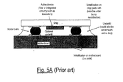
- Flip-chip balls need not be placed directly on the top mirror; a flip-chip ball can also be provided adjacent the top mirror so that the top mirror need only protect against possible surface contaminants such as water vapor. With an off-mirror flip-chip ball, even a single mirror pair usually provides sufficient protection. Between the extremes of three pairs of layers for the top mirror providing full protection and a single pair of layers of material providing protection only against surface contaminants, lies the intermediate case of two pairs of layers, useful if for example underfill material is used so as to come into contact with the top mirror. (As illustrated in Fig. 5, underfill is a glue-like material that is applied between a flipped chip and a motherboard to improve the mechanical reliability of the assembly. The chip is then fastened to the motherboard not only by the solder balls, but also by the underfill material.)
- top acoustic mirror There are, of course, several ways to construct a top acoustic mirror. Two examples are described below, one with three pairs of layers for the top mirror, and flip-chip balls on top of the mirrors, and another with only one pair of layers of material for the top mirror and an off-mirror flip-chip ball.
- a BAW resonator according to the present invention is shown as including both a bottom mirror (Fig. 2A) and a top mirror (Fig. 2D) with a flip-chip ball affixed atop the top mirror.
- the piezolayer is deposited and, if required, patterned, as shown in Fig. 2A. Then, as shown in Fig.
- a thick passivation layer is deposited, and a channel is formed through the passivation layer extending down to the top of the piezolayer (or down to the top electrode); the channel is of a size so that the passivation material is removed essentially everywhere above the piezolayer.
- the top electrode and other optional layers are not shown, such as a shunt tuning layer. The top electrode would usually be deposited before the passivation layer.
- Fig. 2C all the top mirror layers are deposited, one after the other. Once all the top layers have been deposited, the metallic layers of the top mirror are patterned (i.e. selectively removed everywhere except immediately above the piezolayer).
- a wire bonded to the top mirror of the resonator may be used as a way of connecting the resonator to a circuit.
- the wire is connected to the top electrode, beneath the top mirror, through the electrically conductive mirror (the conductive mirror thereby serving not only as a mirror, but also as a kind of a via).
- the conductive mirror in such an embodiment serves as a pad for bumps or bond wires and also providing a connection to the surface of the piezolayer.
- the die can be sawed and wire-bonded as is.
- Any IC chip such as the BAW filters of the present invention, must be provided with a means of being electrically connected to a circuit.
- IC chips are often first wire-bonded to a lead frame and then plastic molded, resulting in a ready packaged component.
- Wire bonding is a method where, by use of 25 to 50 ⁇ m thick gold or silver wire, the IC input/output terminals are connected to the package input/output pins. The more modern method is the flip chip method, described above, where the connections created by wire bonds are replaced by solder bumps.)
- the inventors constructed a receiver filter consisting of six resonators (three series resonators and three shunt resonators) based on double-layer acoustic mirror-type BAW resonators fabricated according to the above description.
- the interconnections from resonator to resonator were created using the bottom electrode metal and an additional metal on top of the finished top mirror, such as, for example, the under bump metal, or, in some cases, an additional top electrode metal on top of the piezolayer, below the top mirror.
- the terminology under bump metal is used for the metal layers between the I/O pads of an integrated chip; these metal layers are used to ensure chemical (metallurgical) compatibility of the solder ball with the I/O pads.
- the shunt resonators were fabricated according to the same process, except for including an additional layer to decrease the resonant frequency so as to obtain the desired bandpass behavior of the filter.
- the additional layer was placed on top of the additional top electrode, but could have been placed below the bottom electrode.
- the top mirror included three pairs of tungsten/aluminum layer pairs; a thin copper tuning layer for (only) the shunt resonator; an aluminum top electrode; a zinc oxide piezolayer; and a gold bottom electrode. Both resonators then included a bottom acoustic mirror consisting of two pairs of layers, one layer being silicon dioxide and the other layer being tungsten.
- the filter so constructed was a ladder-type BAW filter, consisting of three BAW filters connected in series, each BAW filter consisting of a series resonator and a shunt resonator.
- a schematic of the filter is shown in Fig. 3A, and the response of the filter is shown in Fig. 3B.
- the filter response was characteristic of a bandpass filter, with the maximum response centered at approximately 942 MHz, and with a bandwidth of approximately 35 MHz.
- Fig. 4 shows part of a BAW filter (a shunt resonator and a series resonator) mounted on a single substrate, each BAW resonator fabricated according to the invention so as to include two acoustic mirrors.
- the two BAW resonators are shown interconnected through the top electrode.
- a flip-chip ball (for use in providing a signal port of the filter) is shown offset from either top mirror, and connected to one top mirror through a thin metallic layer. The interconnection of the resonators is shown being made using the top electrode.
- One problem in fabricating a top mirror is how to stop the etching of the thick passivation layer during the channel creation step exactly at the surface of the piezolayer.
- One solution is to deposit and pattern a thin top electrode, on top of the piezolayer, prior to depositing the thick passivation layer. Doing so gives good selectivity, i.e. a significantly different etch rate for different materials.
- _in order to stop removing material as soon as reaching the top electrode on the piezolayer it is desirable to have a high etch rate for the passivation layer and a low etch rate for the top electrode. Then once the etching (wet or dry) reaches the surface of the top electrode, it slows to such an extent that it can be said to have stopped.
- Another problem is that the layers of a BAW resonator, especially the piezolayer, tend not to be of uniform thickness, and so there are variations across the wafer in the center frequency of a filter made of BAW resonators fabricated according to the prior art.
- the variation in the thickness of BAW layers can be compensated for by selectively depositing or removing material from areas where the frequency error is unacceptably large. Such adjusting can be performed on prior art resonators, but the thickness of the material that is to be removed or added is typically quite small.
- the use of a top mirror with only two layers has the advantage over the prior art that a BAW resonator so fabricated is fairly insensitive to surface contaminants on top of the top mirror.
- adding or removing material to a structure can only be accomplished to within some absolute error (an error that varies significantly, depending on the material being deposited and the equipment being used) so that adding (or removing) more material has a smaller relative error than adding (or removing) less material, frequency trimming by adding material to a relatively thick top mirror can be performed with a relatively small relative error.
- the frequency trimming would have a relative accuracy of 10%; whereas, in adding material on top of a top mirror, the required overall thickness might be 80nm, which would again be deposited with an absolute error of 2nm, providing a relative accuracy of 21 ⁇ 2%.
- the present invention also comprehends providing a bridge-type BAW resonator with an acoustic mirror on top of the resonator, although in the experience of the inventors, the preferred embodiment is a two-acoustic mirror (top and bottom mirrors) BAW resonator.
- a bridge-type BAW resonator with an acoustic mirror on top of the resonator, although in the experience of the inventors, the preferred embodiment is a two-acoustic mirror (top and bottom mirrors) BAW resonator.
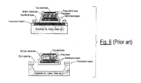
- Two kinds of bridge-type BAW resonators according to the prior art are shown in Fig. 6. Referring now to Fig.
- a bridge-type BAW resonator with a covering conductive acoustic mirror, first the resonator (including the membrane and the cavity underneath the membrane) is fabricated, and then the rest of the fabrication is performed in a way that is essentially identical to what is done in providing a BAW resonator with a bottom acoustic mirror instead of a membrane.
- the membrane of a bridge-type BAW resonator is another type of isolation structure.
- the present invention also comprehends making a BAW resonator with a bottom acoustic mirror, where the bottom mirror is made to be conductive (i.e. made out of only metallic layers) and then to make use of one or another kind of wafer level packaging.
- the resonators are fabricated as usual (with a bottom acoustic mirror) except for using only metals in the bottom mirror, but no top mirror is provided.
- a capping wafer is attached to the top of the wafer containing the filters.
- the capping wafer has small pits in places of the filter to provide an air space above each filter active area (resonator).
- the capping wafer is attached to the filter wafer by anodic bonding, or by glue, or by solder. After the two wafers are joined, the original filter wafer is thinned and/or vias are opened from the backside to gain access to the bottommost layer of the conductive mirrors. The vias are then filled with solder balls, which then serve as the signal ports of the package.
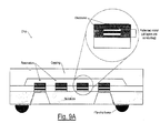
- Fig. 9A provides an elevation view of a wafer-level package of bulk wave resonators such as shown in Fig. 8, a package with off-mirror flip-chip bumps.
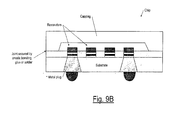
- Fig. 9B is an elevation view of a wafer-level package of bulk wave resonators such as shown in Fig. 8, a package with on-mirror flip-chip bumps.
- the capping shown in Figs. 9A and 9B provides protection of the filter against mechanical loading.
- One of the problems of using a double-mirror resonator as one component of a filter (whether either mirror is all-conductive or not) is that the achievable bandwidth of the filter is somewhat narrower than for a filter including a resonator using only one mirror. Therefore any structure including resonators using only one mirror, but at the same providing protection by for example including a capping wafer such as shown in Figs. 9A and 9B, is in some cases preferable.
Landscapes
- Physics & Mathematics (AREA)
- Acoustics & Sound (AREA)
- Engineering & Computer Science (AREA)
- Manufacturing & Machinery (AREA)
- Piezo-Electric Or Mechanical Vibrators, Or Delay Or Filter Circuits (AREA)
- Electromechanical Clocks (AREA)
Abstract
Description
Claims (16)
- A method of fabricating a bulk acoustic wave (BAW) resonator, comprising the steps of:wherein the first isolation structure comprises an acoustic mirror made from only electrically conductive layers of alternating high and low acoustic impedance.a) providing a substrate;b) providing a first isolation structure; andc) providing a resonator section, the resonator section comprising a piezolayer;
- The method of claim 1, wherein a layer of the acoustic mirror abuts the piezolayer and serves as an electrode.
- A method as in claim 1 or 2, wherein the first isolation structure is situated between the resonator section and the substrate.
- A method as in claim 1, 2 or 3, wherein the first isolation structure is provided so as to be situated above the resonator section, on the side of the resonator section facing away from the substrate, so that the resonator section lies between the first isolation structure and the substrate, and the method further comprises the step of providing a second isolation structure situated between the resonator section and the substrate.
- A method as in claim 4, wherein the second isolation structure comprises an acoustic mirror made from layers of materials of alternating high and low acoustic impedance.
- A method as in claim 4, wherein the second isolation structure comprises a membrane.
- A method as in claim 4, 5 or 6, further comprising the step of providing a flip-chip ball on top of the first isolation structure.
- A method as in any preceding claim, further comprising the step of providing a capping material, the capping material positioned so that the first isolation structure and resonator section are sandwiched between the substrate and the capping material and so protected against mechanical loading, with an air interface between the resonator section and either the capping material or the substrate in case of the resonator including only a single isolation structure.
- A bulk acoustic wave (BAW) resonator, comprising:wherein the first isolation structure comprises an acoustic mirror made from only electrically conductive layers of alternating high and low acoustic impedance.a) a substrate;b) a first isolation structure; andc) a resonator section, the resonator section comprising a piezolayer;
- A BAW resonator as in claim 9, wherein a layer of the acoustic mirror abuts the piezolayer and serves as an electrode.
- A BAW resonator as in claim 9 or 10, wherein the first isolation structure is situated between the resonator section and the substrate.
- A BAW resonator as in claim 9 or 10, wherein the first isolation structure is situated above the resonator section, on the side of the resonator section facing away from the substrate, so that the resonator section lies between the first isolation structure and the substrate, and further comprising a second isolation structure situated between the resonator section and the substrate.
- A BAW resonator as in claim 12, wherein the second isolation structure comprises an acoustic mirror made from layers of materials of alternating high and low acoustic impedance.
- A BAW resonator as in claim 12, wherein the second isolation structure comprises a membrane.
- A BAW resonator as in claim 12, 13 or 14. further comprising a flip-chip ball on top of the first isolation structure.
- A BAW resonator as in any of claims 9 to 15, further comprising a capping material, the capping material positioned so that the first isolation structure and resonator section are sandwiched between the substrate and the capping material and so protected against mechanical loading, with an air interface between the resonator section and either the capping material or the substrate in case of the resonator including only a single isolation structure.
Applications Claiming Priority (2)
| Application Number | Priority Date | Filing Date | Title |
|---|---|---|---|
| US09/761,171 US6509813B2 (en) | 2001-01-16 | 2001-01-16 | Bulk acoustic wave resonator with a conductive mirror |
| US761171 | 2001-01-16 |
Publications (3)
| Publication Number | Publication Date |
|---|---|
| EP1227581A2 true EP1227581A2 (en) | 2002-07-31 |
| EP1227581A3 EP1227581A3 (en) | 2004-12-15 |
| EP1227581B1 EP1227581B1 (en) | 2008-12-24 |
Family
ID=25061382
Family Applications (1)
| Application Number | Title | Priority Date | Filing Date |
|---|---|---|---|
| EP02250263A Expired - Lifetime EP1227581B1 (en) | 2001-01-16 | 2002-01-15 | Bulk acoustic wave resonator with a conductive acoustic mirror |
Country Status (5)
| Country | Link |
|---|---|
| US (1) | US6509813B2 (en) |
| EP (1) | EP1227581B1 (en) |
| JP (1) | JP4248180B2 (en) |
| AT (1) | ATE418813T1 (en) |
| DE (1) | DE60230462D1 (en) |
Cited By (1)
| Publication number | Priority date | Publication date | Assignee | Title |
|---|---|---|---|---|
| WO2018111532A1 (en) * | 2016-12-13 | 2018-06-21 | Snaptrack, Inc. | Baw resonator device |
Families Citing this family (58)
| Publication number | Priority date | Publication date | Assignee | Title |
|---|---|---|---|---|
| US6778038B2 (en) * | 2001-10-05 | 2004-08-17 | Tdk Corporation | Piezoelectric resonant filter, duplexer, and method of manufacturing same |
| US20100107389A1 (en) * | 2002-01-11 | 2010-05-06 | Avago Technologies Wireless Ip (Singapore) Pte. Ltd. | Method of fabricating an electrode for a bulk acoustic resonator |
| DE10200741A1 (en) * | 2002-01-11 | 2003-07-24 | Infineon Technologies Ag | Process for the production of a topology-optimized electrode for a resonator using thin-film technology |
| US7989851B2 (en) * | 2002-06-06 | 2011-08-02 | Rutgers, The State University Of New Jersey | Multifunctional biosensor based on ZnO nanostructures |
| US8377683B2 (en) | 2002-06-06 | 2013-02-19 | Rutgers, The State University Of New Jersey | Zinc oxide-based nanostructure modified QCM for dynamic monitoring of cell adhesion and proliferation |
| DE20221966U1 (en) * | 2002-06-06 | 2010-02-25 | Epcos Ag | Acoustic wave device with a matching network |
| JP2004120016A (en) * | 2002-09-20 | 2004-04-15 | Fujitsu Media Device Kk | Filter device |
| JP4128836B2 (en) * | 2002-09-27 | 2008-07-30 | Tdk株式会社 | Thin film piezoelectric resonator, filter and duplexer using the same |
| FR2848036B1 (en) * | 2002-11-28 | 2005-08-26 | St Microelectronics Sa | SUPPORT FOR ACOUSTIC RESONATOR, ACOUSTIC RESONATOR AND CORRESPONDING INTEGRATED CIRCUIT |
| KR100517841B1 (en) * | 2003-02-22 | 2005-09-30 | 주식회사 엠에스솔루션 | FBAR band pass filter, Duplexer having the FBAR band pass filter and Methods for manufacturing the same |
| EP1469599B1 (en) * | 2003-04-18 | 2010-11-03 | Samsung Electronics Co., Ltd. | Air gap type FBAR, duplexer using the FBAR, and fabricating methods thereof |
| DE10331322A1 (en) * | 2003-07-10 | 2005-02-03 | Epcos Ag | Electronic component and method of manufacture |
| KR100616511B1 (en) * | 2003-09-24 | 2006-08-29 | 삼성전기주식회사 | FARA element and its manufacturing method |
| KR100519816B1 (en) * | 2003-09-29 | 2005-10-10 | 삼성전기주식회사 | FBAR duplexer device and packaging method thereof |
| KR100555762B1 (en) * | 2003-10-07 | 2006-03-03 | 삼성전자주식회사 | Air gap type thin film bulk acoustic resonator and its manufacturing method, filter and duplexer using same |
| JP2005129610A (en) * | 2003-10-22 | 2005-05-19 | Tdk Corp | Electronic components |
| JP2005136683A (en) * | 2003-10-30 | 2005-05-26 | Tdk Corp | Electronic components |
| JP2005167969A (en) * | 2003-11-14 | 2005-06-23 | Fujitsu Media Device Kk | Acoustic wave device and method of manufacturing acoustic wave device |
| JP2005151287A (en) * | 2003-11-18 | 2005-06-09 | Tdk Corp | Electronic components |
| FR2863789B1 (en) * | 2003-12-12 | 2006-09-29 | St Microelectronics Sa | ACOUSTIC RESONATOR DEVICE |
| US6992400B2 (en) | 2004-01-30 | 2006-01-31 | Nokia Corporation | Encapsulated electronics device with improved heat dissipation |
| US7227433B2 (en) * | 2004-03-31 | 2007-06-05 | Intel Corporation | Electro mechanical device having a sealed cavity |
| JP4375399B2 (en) * | 2004-07-20 | 2009-12-02 | 株式会社村田製作所 | Piezoelectric filter |
| JP4693397B2 (en) * | 2004-11-26 | 2011-06-01 | 京セラ株式会社 | Thin film bulk acoustic wave resonator and filter, and communication device |
| JP4016983B2 (en) | 2004-12-07 | 2007-12-05 | 株式会社村田製作所 | Piezoelectric thin film resonator and manufacturing method thereof |
| JP2006191304A (en) * | 2005-01-05 | 2006-07-20 | Matsushita Electric Ind Co Ltd | Piezoelectric resonator and manufacturing method thereof |
| DE102005004435B4 (en) * | 2005-01-31 | 2006-10-19 | Infineon Technologies Ag | BAW RESONATOR |
| DE102005006833B4 (en) * | 2005-02-15 | 2017-02-23 | Epcos Ag | Method for producing a BAW component and BAW component |
| FR2890490A1 (en) * | 2005-09-05 | 2007-03-09 | St Microelectronics Sa | ACOUSTIC RESONATOR SUPPORT AND CORRESPONDING INTEGRATED CIRCUIT |
| DE102005044330A1 (en) * | 2005-09-16 | 2007-03-29 | Epcos Ag | Tunable capacitor and circuit with such a capacitor |
| JP5096695B2 (en) * | 2006-05-30 | 2012-12-12 | パナソニック株式会社 | Thin film acoustic resonator |
| US8212331B1 (en) * | 2006-10-02 | 2012-07-03 | Newport Fab, Llc | Method for fabricating a backside through-wafer via in a processed wafer and related structure |
| US7851333B2 (en) * | 2007-03-15 | 2010-12-14 | Infineon Technologies Ag | Apparatus comprising a device and method for producing it |
| US8514033B2 (en) * | 2007-10-18 | 2013-08-20 | Avago Technologies General Ip (Singapore) Pte. Ltd. | BAW structure with reduced topographic steps and related method |
| US8410868B2 (en) * | 2009-06-04 | 2013-04-02 | Sand 9, Inc. | Methods and apparatus for temperature control of devices and mechanical resonating structures |
| US8476809B2 (en) | 2008-04-29 | 2013-07-02 | Sand 9, Inc. | Microelectromechanical systems (MEMS) resonators and related apparatus and methods |
| US9048811B2 (en) | 2009-03-31 | 2015-06-02 | Sand 9, Inc. | Integration of piezoelectric materials with substrates |
| DE102009018879B4 (en) * | 2009-04-24 | 2016-03-17 | Epcos Ag | Bottom electrode for Bulk Acoustic Wave (BAW) resonator |
| US20110121916A1 (en) * | 2009-11-24 | 2011-05-26 | Avago Technologies Wireless Ip (Singapore) Pte. Ltd. | Hybrid bulk acoustic wave resonator |
| US8922302B2 (en) | 2011-08-24 | 2014-12-30 | Avago Technologies General Ip (Singapore) Pte. Ltd. | Acoustic resonator formed on a pedestal |
| US9246467B2 (en) * | 2012-05-31 | 2016-01-26 | Texas Instruments Incorporated | Integrated resonator with a mass bias |
| KR101959204B1 (en) * | 2013-01-09 | 2019-07-04 | 삼성전자주식회사 | Radio frequency filter and manufacturing mathod thereof |
| US10658998B2 (en) | 2013-07-31 | 2020-05-19 | Oepic Semiconductors, Inc. | Piezoelectric film transfer for acoustic resonators and filters |
| WO2016147986A1 (en) * | 2015-03-16 | 2016-09-22 | 株式会社村田製作所 | Elastic wave device and production method for same |
| US20160329481A1 (en) * | 2015-05-04 | 2016-11-10 | Samsung Electro-Mechanics Co., Ltd. | Bulk acoustic wave resonator and filter including the same |
| US10135415B2 (en) * | 2015-12-18 | 2018-11-20 | Texas Instruments Incorporated | Method to reduce frequency distribution of bulk acoustic wave resonators during manufacturing |
| CN110231407B (en) * | 2018-03-06 | 2022-02-15 | 中国石油化工股份有限公司 | Method for judging effectiveness of carbonate rock cover layer |
| US10985729B2 (en) * | 2018-12-28 | 2021-04-20 | Texas Instruments Incorporated | BAW resonator based pressure sensor |
| WO2020227396A1 (en) * | 2019-05-06 | 2020-11-12 | Qorvo Biotechnologies, Llc | Acoustic resonator device |
| US12431861B2 (en) | 2019-07-31 | 2025-09-30 | Qxoniix Inc. | Layers, structures, acoustic wave resonators, devices and systems |
| US12451860B2 (en) | 2019-07-31 | 2025-10-21 | QXONIX Inc. | Structures, acoustic wave resonators, devices and systems |
| WO2021021723A1 (en) | 2019-07-31 | 2021-02-04 | QXONIX Inc. | Acoustic device structures, devices and systems |
| US12445109B2 (en) | 2019-07-31 | 2025-10-14 | QXONIX Inc. | Structures, acoustic wave resonators, layers, devices and systems |
| US11463065B2 (en) | 2019-12-03 | 2022-10-04 | Skyworks Solutions, Inc. | Laterally excited bulk wave device with acoustic mirror |
| US20220321088A1 (en) | 2021-03-31 | 2022-10-06 | Skyworks Solutions, Inc. | Acoustic wave device with double side acoustic mirror |
| US12615033B2 (en) * | 2021-10-04 | 2026-04-28 | Skyworks Solutions, Inc. | Stacked single mirror acoustic wave device and double mirror acoustic wave device |
| US12531541B2 (en) | 2021-10-05 | 2026-01-20 | Skyworks Solutions, Inc. | Stacked structure with multiple acoustic wave devices |
| JP2025115838A (en) * | 2024-01-26 | 2025-08-07 | 株式会社D‐process | Bulk Acoustic Wave Devices |
Family Cites Families (10)
| Publication number | Priority date | Publication date | Assignee | Title |
|---|---|---|---|---|
| AT353506B (en) * | 1976-10-19 | 1979-11-26 | List Hans | PIEZOELECTRIC RESONATOR |
| US5373268A (en) * | 1993-02-01 | 1994-12-13 | Motorola, Inc. | Thin film resonator having stacked acoustic reflecting impedance matching layers and method |
| US5864261A (en) * | 1994-05-23 | 1999-01-26 | Iowa State University Research Foundation | Multiple layer acoustical structures for thin-film resonator based circuits and systems |
| US5714917A (en) | 1996-10-02 | 1998-02-03 | Nokia Mobile Phones Limited | Device incorporating a tunable thin film bulk acoustic resonator for performing amplitude and phase modulation |
| US5873154A (en) | 1996-10-17 | 1999-02-23 | Nokia Mobile Phones Limited | Method for fabricating a resonator having an acoustic mirror |
| US6087198A (en) * | 1998-02-12 | 2000-07-11 | Texas Instruments Incorporated | Low cost packaging for thin-film resonators and thin-film resonator-based filters |
| US5872493A (en) * | 1997-03-13 | 1999-02-16 | Nokia Mobile Phones, Ltd. | Bulk acoustic wave (BAW) filter having a top portion that includes a protective acoustic mirror |
| US5910756A (en) | 1997-05-21 | 1999-06-08 | Nokia Mobile Phones Limited | Filters and duplexers utilizing thin film stacked crystal filter structures and thin film bulk acoustic wave resonators |
| FI108583B (en) * | 1998-06-02 | 2002-02-15 | Nokia Corp | resonator structures |
| US6060818A (en) | 1998-06-02 | 2000-05-09 | Hewlett-Packard Company | SBAR structures and method of fabrication of SBAR.FBAR film processing techniques for the manufacturing of SBAR/BAR filters |
-
2001
- 2001-01-16 US US09/761,171 patent/US6509813B2/en not_active Expired - Fee Related
-
2002
- 2002-01-15 JP JP2002006608A patent/JP4248180B2/en not_active Expired - Fee Related
- 2002-01-15 EP EP02250263A patent/EP1227581B1/en not_active Expired - Lifetime
- 2002-01-15 AT AT02250263T patent/ATE418813T1/en not_active IP Right Cessation
- 2002-01-15 DE DE60230462T patent/DE60230462D1/en not_active Expired - Lifetime
Cited By (2)
| Publication number | Priority date | Publication date | Assignee | Title |
|---|---|---|---|---|
| WO2018111532A1 (en) * | 2016-12-13 | 2018-06-21 | Snaptrack, Inc. | Baw resonator device |
| TWI753055B (en) * | 2016-12-13 | 2022-01-21 | 美商史奈帕翠克公司 | Baw resonator device |
Also Published As
| Publication number | Publication date |
|---|---|
| EP1227581A3 (en) | 2004-12-15 |
| US20020093398A1 (en) | 2002-07-18 |
| ATE418813T1 (en) | 2009-01-15 |
| US6509813B2 (en) | 2003-01-21 |
| DE60230462D1 (en) | 2009-02-05 |
| JP4248180B2 (en) | 2009-04-02 |
| EP1227581B1 (en) | 2008-12-24 |
| JP2002278558A (en) | 2002-09-27 |
Similar Documents
| Publication | Publication Date | Title |
|---|---|---|
| US6509813B2 (en) | Bulk acoustic wave resonator with a conductive mirror | |
| KR100518616B1 (en) | Filter devices and method for fabricating filter devices | |
| JP4212137B2 (en) | Bulk acoustic wave (BAW) filter having a top including a protective acoustic mirror | |
| USRE45419E1 (en) | Surface acoustic wave device and method of fabricating the same | |
| CN104821798B (en) | Electronic Packaging and MEMS package | |
| US20100045145A1 (en) | Piezoelectric component and manufacturing method thereof | |
| JP2007535230A (en) | Method for improving heat dissipation in encapsulated electronic components | |
| JP2005536958A (en) | Resonator and element with hermetic encapsulation member | |
| JP2009188844A (en) | Surface acoustic wave device and manufacturing method thereof | |
| US10651817B2 (en) | Bulk acoustic wave resonator on a stress isolated platform | |
| CN110739391A (en) | Surface acoustic wave filter device and method of manufacturing the same | |
| US11646712B2 (en) | Bulk acoustic wave structure and bulk acoustic wave device | |
| CN107204751B (en) | Electronic component package and method of manufacturing the same | |
| JP4496652B2 (en) | Surface acoustic wave device and manufacturing method thereof | |
| JP7539477B2 (en) | Electronic devices and methods of forming same | |
| CN115001434B (en) | Membrane acoustic resonator with bifurcated electrodes | |
| TWI766476B (en) | Bulk acoustic wave device | |
| JP2005136683A (en) | Electronic components | |
| CN218352484U (en) | Semiconductor packaging structure | |
| CN120263131A (en) | Bulk acoustic wave device manufacturing method, device and bulk acoustic wave device | |
| CN114337579A (en) | Resonance device, manufacturing method thereof and integrated circuit board integrated with resonance device | |
| JP3874709B2 (en) | Semiconductor element and semiconductor device | |
| CN120263130A (en) | Bulk acoustic wave device manufacturing method and bulk acoustic wave device | |
| CN117294279A (en) | Wafer-level packaged surface acoustic wave filter and manufacturing method thereof | |
| CN114499437A (en) | Electronic component and elastic wave device |
Legal Events
| Date | Code | Title | Description |
|---|---|---|---|
| PUAI | Public reference made under article 153(3) epc to a published international application that has entered the european phase |
Free format text: ORIGINAL CODE: 0009012 |
|
| AK | Designated contracting states |
Kind code of ref document: A2 Designated state(s): AT BE CH CY DE DK ES FI FR GB GR IE IT LI LU MC NL PT SE TR |
|
| AX | Request for extension of the european patent |
Free format text: AL;LT;LV;MK;RO;SI |
|
| PUAL | Search report despatched |
Free format text: ORIGINAL CODE: 0009013 |
|
| AK | Designated contracting states |
Kind code of ref document: A3 Designated state(s): AT BE CH CY DE DK ES FI FR GB GR IE IT LI LU MC NL PT SE TR |
|
| AX | Request for extension of the european patent |
Extension state: AL LT LV MK RO SI |
|
| 17P | Request for examination filed |
Effective date: 20050609 |
|
| AKX | Designation fees paid |
Designated state(s): AT BE CH CY DE DK ES FI FR GB GR IE IT LI LU MC NL PT SE TR |
|
| 17Q | First examination report despatched |
Effective date: 20060718 |
|
| GRAP | Despatch of communication of intention to grant a patent |
Free format text: ORIGINAL CODE: EPIDOSNIGR1 |
|
| RAP1 | Party data changed (applicant data changed or rights of an application transferred) |
Owner name: AVAGO TECHNOLOGIES WIRELESS IP (SINGAPORE) PTE. LT |
|
| GRAS | Grant fee paid |
Free format text: ORIGINAL CODE: EPIDOSNIGR3 |
|
| GRAA | (expected) grant |
Free format text: ORIGINAL CODE: 0009210 |
|
| AK | Designated contracting states |
Kind code of ref document: B1 Designated state(s): AT BE CH CY DE DK ES FI FR GB GR IE IT LI LU MC NL PT SE TR |
|
| REG | Reference to a national code |
Ref country code: GB Ref legal event code: FG4D |
|
| REG | Reference to a national code |
Ref country code: CH Ref legal event code: EP |
|
| REG | Reference to a national code |
Ref country code: IE Ref legal event code: FG4D |
|
| REF | Corresponds to: |
Ref document number: 60230462 Country of ref document: DE Date of ref document: 20090205 Kind code of ref document: P |
|
| PG25 | Lapsed in a contracting state [announced via postgrant information from national office to epo] |
Ref country code: NL Free format text: LAPSE BECAUSE OF FAILURE TO SUBMIT A TRANSLATION OF THE DESCRIPTION OR TO PAY THE FEE WITHIN THE PRESCRIBED TIME-LIMIT Effective date: 20081224 Ref country code: FI Free format text: LAPSE BECAUSE OF FAILURE TO SUBMIT A TRANSLATION OF THE DESCRIPTION OR TO PAY THE FEE WITHIN THE PRESCRIBED TIME-LIMIT Effective date: 20081224 |
|
| NLV1 | Nl: lapsed or annulled due to failure to fulfill the requirements of art. 29p and 29m of the patents act | ||
| PG25 | Lapsed in a contracting state [announced via postgrant information from national office to epo] |
Ref country code: BE Free format text: LAPSE BECAUSE OF FAILURE TO SUBMIT A TRANSLATION OF THE DESCRIPTION OR TO PAY THE FEE WITHIN THE PRESCRIBED TIME-LIMIT Effective date: 20081224 Ref country code: ES Free format text: LAPSE BECAUSE OF FAILURE TO SUBMIT A TRANSLATION OF THE DESCRIPTION OR TO PAY THE FEE WITHIN THE PRESCRIBED TIME-LIMIT Effective date: 20090404 |
|
| PG25 | Lapsed in a contracting state [announced via postgrant information from national office to epo] |
Ref country code: PT Free format text: LAPSE BECAUSE OF FAILURE TO SUBMIT A TRANSLATION OF THE DESCRIPTION OR TO PAY THE FEE WITHIN THE PRESCRIBED TIME-LIMIT Effective date: 20090525 Ref country code: MC Free format text: LAPSE BECAUSE OF NON-PAYMENT OF DUE FEES Effective date: 20090131 Ref country code: SE Free format text: LAPSE BECAUSE OF FAILURE TO SUBMIT A TRANSLATION OF THE DESCRIPTION OR TO PAY THE FEE WITHIN THE PRESCRIBED TIME-LIMIT Effective date: 20090324 Ref country code: AT Free format text: LAPSE BECAUSE OF FAILURE TO SUBMIT A TRANSLATION OF THE DESCRIPTION OR TO PAY THE FEE WITHIN THE PRESCRIBED TIME-LIMIT Effective date: 20081224 |
|
| REG | Reference to a national code |
Ref country code: CH Ref legal event code: PL |
|
| REG | Reference to a national code |
Ref country code: IE Ref legal event code: MM4A |
|
| PG25 | Lapsed in a contracting state [announced via postgrant information from national office to epo] |
Ref country code: DK Free format text: LAPSE BECAUSE OF FAILURE TO SUBMIT A TRANSLATION OF THE DESCRIPTION OR TO PAY THE FEE WITHIN THE PRESCRIBED TIME-LIMIT Effective date: 20081224 Ref country code: LI Free format text: LAPSE BECAUSE OF NON-PAYMENT OF DUE FEES Effective date: 20090131 Ref country code: CH Free format text: LAPSE BECAUSE OF NON-PAYMENT OF DUE FEES Effective date: 20090131 |
|
| PLBE | No opposition filed within time limit |
Free format text: ORIGINAL CODE: 0009261 |
|
| STAA | Information on the status of an ep patent application or granted ep patent |
Free format text: STATUS: NO OPPOSITION FILED WITHIN TIME LIMIT |
|
| GBPC | Gb: european patent ceased through non-payment of renewal fee |
Effective date: 20090324 |
|
| REG | Reference to a national code |
Ref country code: FR Ref legal event code: ST Effective date: 20091030 |
|
| 26N | No opposition filed |
Effective date: 20090925 |
|
| PG25 | Lapsed in a contracting state [announced via postgrant information from national office to epo] |
Ref country code: IE Free format text: LAPSE BECAUSE OF NON-PAYMENT OF DUE FEES Effective date: 20090115 |
|
| PG25 | Lapsed in a contracting state [announced via postgrant information from national office to epo] |
Ref country code: FR Free format text: LAPSE BECAUSE OF NON-PAYMENT OF DUE FEES Effective date: 20090224 Ref country code: GB Free format text: LAPSE BECAUSE OF NON-PAYMENT OF DUE FEES Effective date: 20090324 |
|
| PG25 | Lapsed in a contracting state [announced via postgrant information from national office to epo] |
Ref country code: GR Free format text: LAPSE BECAUSE OF FAILURE TO SUBMIT A TRANSLATION OF THE DESCRIPTION OR TO PAY THE FEE WITHIN THE PRESCRIBED TIME-LIMIT Effective date: 20090325 |
|
| PG25 | Lapsed in a contracting state [announced via postgrant information from national office to epo] |
Ref country code: IT Free format text: LAPSE BECAUSE OF FAILURE TO SUBMIT A TRANSLATION OF THE DESCRIPTION OR TO PAY THE FEE WITHIN THE PRESCRIBED TIME-LIMIT Effective date: 20081224 |
|
| PG25 | Lapsed in a contracting state [announced via postgrant information from national office to epo] |
Ref country code: LU Free format text: LAPSE BECAUSE OF NON-PAYMENT OF DUE FEES Effective date: 20090115 |
|
| PG25 | Lapsed in a contracting state [announced via postgrant information from national office to epo] |
Ref country code: TR Free format text: LAPSE BECAUSE OF FAILURE TO SUBMIT A TRANSLATION OF THE DESCRIPTION OR TO PAY THE FEE WITHIN THE PRESCRIBED TIME-LIMIT Effective date: 20081224 |
|
| PG25 | Lapsed in a contracting state [announced via postgrant information from national office to epo] |
Ref country code: CY Free format text: LAPSE BECAUSE OF FAILURE TO SUBMIT A TRANSLATION OF THE DESCRIPTION OR TO PAY THE FEE WITHIN THE PRESCRIBED TIME-LIMIT Effective date: 20081224 |
|
| PGFP | Annual fee paid to national office [announced via postgrant information from national office to epo] |
Ref country code: DE Payment date: 20130109 Year of fee payment: 12 |
|
| REG | Reference to a national code |
Ref country code: DE Ref legal event code: R082 Ref document number: 60230462 Country of ref document: DE Representative=s name: DILG HAEUSLER SCHINDELMANN PATENTANWALTSGESELL, DE |
|
| REG | Reference to a national code |
Ref country code: DE Ref legal event code: R082 Ref document number: 60230462 Country of ref document: DE Representative=s name: DILG HAEUSLER SCHINDELMANN PATENTANWALTSGESELL, DE Effective date: 20130605 Ref country code: DE Ref legal event code: R081 Ref document number: 60230462 Country of ref document: DE Owner name: AVAGO TECHNOLOGIES GENERAL IP (SINGAPORE) PTE., SG Free format text: FORMER OWNER: AVAGO TECHNOLOGIES WIRELESS IP (SINGAPORE) PTE. LTD., SINGAPORE, SG Effective date: 20130605 |
|
| REG | Reference to a national code |
Ref country code: DE Ref legal event code: R119 Ref document number: 60230462 Country of ref document: DE |
|
| REG | Reference to a national code |
Ref country code: DE Ref legal event code: R119 Ref document number: 60230462 Country of ref document: DE Effective date: 20140801 |
|
| PG25 | Lapsed in a contracting state [announced via postgrant information from national office to epo] |
Ref country code: DE Free format text: LAPSE BECAUSE OF NON-PAYMENT OF DUE FEES Effective date: 20140801 |