EP1221686B1 - Driving circuit of an active matrix display with compensation of threshold voltage deviation - Google Patents
Driving circuit of an active matrix display with compensation of threshold voltage deviation Download PDFInfo
- Publication number
- EP1221686B1 EP1221686B1 EP02000314A EP02000314A EP1221686B1 EP 1221686 B1 EP1221686 B1 EP 1221686B1 EP 02000314 A EP02000314 A EP 02000314A EP 02000314 A EP02000314 A EP 02000314A EP 1221686 B1 EP1221686 B1 EP 1221686B1
- Authority
- EP
- European Patent Office
- Prior art keywords
- transistor
- switch
- driving circuit
- current
- voltage
- Prior art date
- Legal status (The legal status is an assumption and is not a legal conclusion. Google has not performed a legal analysis and makes no representation as to the accuracy of the status listed.)
- Expired - Lifetime
Links
Images




Classifications
-
- G—PHYSICS
- G09—EDUCATION; CRYPTOGRAPHY; DISPLAY; ADVERTISING; SEALS
- G09G—ARRANGEMENTS OR CIRCUITS FOR CONTROL OF INDICATING DEVICES USING STATIC MEANS TO PRESENT VARIABLE INFORMATION
- G09G3/00—Control arrangements or circuits, of interest only in connection with visual indicators other than cathode-ray tubes
- G09G3/20—Control arrangements or circuits, of interest only in connection with visual indicators other than cathode-ray tubes for presentation of an assembly of a number of characters, e.g. a page, by composing the assembly by combination of individual elements arranged in a matrix no fixed position being assigned to or needed to be assigned to the individual characters or partial characters
- G09G3/22—Control arrangements or circuits, of interest only in connection with visual indicators other than cathode-ray tubes for presentation of an assembly of a number of characters, e.g. a page, by composing the assembly by combination of individual elements arranged in a matrix no fixed position being assigned to or needed to be assigned to the individual characters or partial characters using controlled light sources
- G09G3/30—Control arrangements or circuits, of interest only in connection with visual indicators other than cathode-ray tubes for presentation of an assembly of a number of characters, e.g. a page, by composing the assembly by combination of individual elements arranged in a matrix no fixed position being assigned to or needed to be assigned to the individual characters or partial characters using controlled light sources using electroluminescent panels
- G09G3/32—Control arrangements or circuits, of interest only in connection with visual indicators other than cathode-ray tubes for presentation of an assembly of a number of characters, e.g. a page, by composing the assembly by combination of individual elements arranged in a matrix no fixed position being assigned to or needed to be assigned to the individual characters or partial characters using controlled light sources using electroluminescent panels semiconductive, e.g. using light-emitting diodes [LED]
- G09G3/3208—Control arrangements or circuits, of interest only in connection with visual indicators other than cathode-ray tubes for presentation of an assembly of a number of characters, e.g. a page, by composing the assembly by combination of individual elements arranged in a matrix no fixed position being assigned to or needed to be assigned to the individual characters or partial characters using controlled light sources using electroluminescent panels semiconductive, e.g. using light-emitting diodes [LED] organic, e.g. using organic light-emitting diodes [OLED]
- G09G3/3225—Control arrangements or circuits, of interest only in connection with visual indicators other than cathode-ray tubes for presentation of an assembly of a number of characters, e.g. a page, by composing the assembly by combination of individual elements arranged in a matrix no fixed position being assigned to or needed to be assigned to the individual characters or partial characters using controlled light sources using electroluminescent panels semiconductive, e.g. using light-emitting diodes [LED] organic, e.g. using organic light-emitting diodes [OLED] using an active matrix
- G09G3/3233—Control arrangements or circuits, of interest only in connection with visual indicators other than cathode-ray tubes for presentation of an assembly of a number of characters, e.g. a page, by composing the assembly by combination of individual elements arranged in a matrix no fixed position being assigned to or needed to be assigned to the individual characters or partial characters using controlled light sources using electroluminescent panels semiconductive, e.g. using light-emitting diodes [LED] organic, e.g. using organic light-emitting diodes [OLED] using an active matrix with pixel circuitry controlling the current through the light-emitting element
-
- H—ELECTRICITY
- H10—SEMICONDUCTOR DEVICES; ELECTRIC SOLID-STATE DEVICES NOT OTHERWISE PROVIDED FOR
- H10K—ORGANIC ELECTRIC SOLID-STATE DEVICES
- H10K59/00—Integrated devices, or assemblies of multiple devices, comprising at least one organic light-emitting element covered by group H10K50/00
- H10K59/10—OLED displays
- H10K59/12—Active-matrix OLED [AMOLED] displays
- H10K59/121—Active-matrix OLED [AMOLED] displays characterised by the geometry or disposition of pixel elements
- H10K59/1213—Active-matrix OLED [AMOLED] displays characterised by the geometry or disposition of pixel elements the pixel elements being TFTs
-
- H—ELECTRICITY
- H10—SEMICONDUCTOR DEVICES; ELECTRIC SOLID-STATE DEVICES NOT OTHERWISE PROVIDED FOR
- H10K—ORGANIC ELECTRIC SOLID-STATE DEVICES
- H10K59/00—Integrated devices, or assemblies of multiple devices, comprising at least one organic light-emitting element covered by group H10K50/00
- H10K59/10—OLED displays
- H10K59/12—Active-matrix OLED [AMOLED] displays
- H10K59/121—Active-matrix OLED [AMOLED] displays characterised by the geometry or disposition of pixel elements
- H10K59/1216—Active-matrix OLED [AMOLED] displays characterised by the geometry or disposition of pixel elements the pixel elements being capacitors
-
- G—PHYSICS
- G09—EDUCATION; CRYPTOGRAPHY; DISPLAY; ADVERTISING; SEALS
- G09G—ARRANGEMENTS OR CIRCUITS FOR CONTROL OF INDICATING DEVICES USING STATIC MEANS TO PRESENT VARIABLE INFORMATION
- G09G2300/00—Aspects of the constitution of display devices
- G09G2300/08—Active matrix structure, i.e. with use of active elements, inclusive of non-linear two terminal elements, in the pixels together with light emitting or modulating elements
- G09G2300/0809—Several active elements per pixel in active matrix panels
- G09G2300/0833—Several active elements per pixel in active matrix panels forming a linear amplifier or follower
-
- G—PHYSICS
- G09—EDUCATION; CRYPTOGRAPHY; DISPLAY; ADVERTISING; SEALS
- G09G—ARRANGEMENTS OR CIRCUITS FOR CONTROL OF INDICATING DEVICES USING STATIC MEANS TO PRESENT VARIABLE INFORMATION
- G09G2300/00—Aspects of the constitution of display devices
- G09G2300/08—Active matrix structure, i.e. with use of active elements, inclusive of non-linear two terminal elements, in the pixels together with light emitting or modulating elements
- G09G2300/0809—Several active elements per pixel in active matrix panels
- G09G2300/0842—Several active elements per pixel in active matrix panels forming a memory circuit, e.g. a dynamic memory with one capacitor
-
- G—PHYSICS
- G09—EDUCATION; CRYPTOGRAPHY; DISPLAY; ADVERTISING; SEALS
- G09G—ARRANGEMENTS OR CIRCUITS FOR CONTROL OF INDICATING DEVICES USING STATIC MEANS TO PRESENT VARIABLE INFORMATION
- G09G2310/00—Command of the display device
- G09G2310/02—Addressing, scanning or driving the display screen or processing steps related thereto
- G09G2310/0243—Details of the generation of driving signals
- G09G2310/0259—Details of the generation of driving signals with use of an analog or digital ramp generator in the column driver or in the pixel circuit
-
- G—PHYSICS
- G09—EDUCATION; CRYPTOGRAPHY; DISPLAY; ADVERTISING; SEALS
- G09G—ARRANGEMENTS OR CIRCUITS FOR CONTROL OF INDICATING DEVICES USING STATIC MEANS TO PRESENT VARIABLE INFORMATION
- G09G2310/00—Command of the display device
- G09G2310/02—Addressing, scanning or driving the display screen or processing steps related thereto
- G09G2310/0262—The addressing of the pixel, in a display other than an active matrix LCD, involving the control of two or more scan electrodes or two or more data electrodes, e.g. pixel voltage dependent on signals of two data electrodes
-
- G—PHYSICS
- G09—EDUCATION; CRYPTOGRAPHY; DISPLAY; ADVERTISING; SEALS
- G09G—ARRANGEMENTS OR CIRCUITS FOR CONTROL OF INDICATING DEVICES USING STATIC MEANS TO PRESENT VARIABLE INFORMATION
- G09G2310/00—Command of the display device
- G09G2310/06—Details of flat display driving waveforms
- G09G2310/066—Waveforms comprising a gently increasing or decreasing portion, e.g. ramp
-
- G—PHYSICS
- G09—EDUCATION; CRYPTOGRAPHY; DISPLAY; ADVERTISING; SEALS
- G09G—ARRANGEMENTS OR CIRCUITS FOR CONTROL OF INDICATING DEVICES USING STATIC MEANS TO PRESENT VARIABLE INFORMATION
- G09G2320/00—Control of display operating conditions
- G09G2320/02—Improving the quality of display appearance
- G09G2320/029—Improving the quality of display appearance by monitoring one or more pixels in the display panel, e.g. by monitoring a fixed reference pixel
-
- G—PHYSICS
- G09—EDUCATION; CRYPTOGRAPHY; DISPLAY; ADVERTISING; SEALS
- G09G—ARRANGEMENTS OR CIRCUITS FOR CONTROL OF INDICATING DEVICES USING STATIC MEANS TO PRESENT VARIABLE INFORMATION
- G09G3/00—Control arrangements or circuits, of interest only in connection with visual indicators other than cathode-ray tubes
- G09G3/20—Control arrangements or circuits, of interest only in connection with visual indicators other than cathode-ray tubes for presentation of an assembly of a number of characters, e.g. a page, by composing the assembly by combination of individual elements arranged in a matrix no fixed position being assigned to or needed to be assigned to the individual characters or partial characters
-
- H—ELECTRICITY
- H10—SEMICONDUCTOR DEVICES; ELECTRIC SOLID-STATE DEVICES NOT OTHERWISE PROVIDED FOR
- H10K—ORGANIC ELECTRIC SOLID-STATE DEVICES
- H10K59/00—Integrated devices, or assemblies of multiple devices, comprising at least one organic light-emitting element covered by group H10K50/00
- H10K59/10—OLED displays
- H10K59/12—Active-matrix OLED [AMOLED] displays
Definitions
- the present invention relates to a driving circuit of an active matrix method in a display device.
- the passive matrix method is more efficient.
- the active matrix method is more efficient than the passive matrix method since it is required to use the higher level of current in the passive matrix method than the active matrix method even though a line time is equal.
- FIG. 1 is a circuit diagram of a driving circuit according to a related art active matrix method.
- the driving circuit includes a scan line SEL, a data line, a switch P1, a capacitor Cs, a driving transistor PO, an OEL and a positive power supply VDD.
- the scan line SEL selects a pixel for driving, and the data line applies a voltage to the pixel.
- the switch P1 is served as an active device to control data input according to a signal of the scan line, and the capacitor Cs stores electric charges selected according to the voltage applied to the data line.
- a voltage is input to the driving transistor PO by the electric charges stored in the capacitor Cs, and then the driving transistor PO applies a current to the OEL.
- the OEL emits light by the current applied from the driving transistor PO, and the positive power supply VDD supplies a power to the capacitor Cs and the driving transistor PO.
- the pixel driven by the scan line SEL is selected, and then the pixel for driving is turned on by the switch P1. Then, a control voltage, in which a gray is controlled, is applied to the pixel for driving through the data line.
- control voltage is stored in the capacitor Cs, simultaneously, drives the driving transistor PO to make the OEL emit lights.
- the driving transistor PO is driven by the voltage stored in the capacitor Cs to maintain one frame until the next select time.
- the driving current for driving the OEL selected is not constant even though an equal driving voltage is applied to each driving transistor.
- each OEL emits different luminance according to deviation of the threshold voltages of the driving transistors.
- the deviation of the threshold voltages of the driving transistors is necessary consequence in fabricating process steps of the display device. Therefore, the luminance deviation of the pixels has to be compensated by detecting luminance of each pixel, however, it is hard to effectively compensate the luminance deviation.
- EP-A 1 003 150 relates to transistor circuits including driving transistors for controlling a driving current.
- the compensating transistor has diode characteristics.
- WO 99 65012 A discloses an active matrix electroluminescent display with an array of current-driven electroluminescent display elements comprising organic electroluminescent material, whose operations are each controlled by an associated switching means to which a drive signal for determining a desired light output is supplied in a respective address period and which is arranged to drive the display element according to the drive signal following the address period.
- Each switching means comprises a current mirror circuit which samples and stores the drive signal and comprises a first transistor whose current-carrying electrodes are connected between a supply line and an electrode of the display element, a second transistor to whose gate electrode and first current-carrying electrode the drive signal is applied and whose second current-carrying electrode is connected to the supply line.
- the gate of the first transistor is connected to the supply line via a storage capacitor and to the gate of the second transistor via a switch device which is operable to connect the gates of the first and second transistors during the address period.
- EP-A 0 905 673 discloses an active matrix display system with a LED or an OLED pixel structure with five transistors. This structure determines an offset voltage parameter using an autozeroing method which comprises a precharge phase, a auto-zero phase and a data writing phase.
- the auto-zero phase is essentially a current-drive mode of operation, where the drive current is very small.
- the writing phase the voltage on the LED is incremented above turn-on using the applied data voltage.
- a first switch or transistor connectable to a data line and to a scan line, which is adapted to switch an externally applied control voltage
- a driving unit C1, MN2
- its input being connected to the output of the first switch and adapted to store the control voltage applied by switching of the first switch
- an emitting pixel OLED
- a second switch (MN3), which is adapted for switching a current applied to the emitting pixel by the control voltage applied from the driving unit directly back to the driving unit, without any further compensating circuitry.
- the present invention is directed to a driving circuit of an active matrix method in a display device that substantially obviates one or more problems due to limitations and disadvantages of the related art.
- An object of the present invention is to provide a driving circuit of an active matrix method in a display device that can constantly improve luminance between pixels.
- a driving circuit of an active matrix display in a display device comprises a first switch connectable to a data line and to a scan line, adapted to switch an externally applied control voltage; a driving unit, its input being connected to the output of the first switch and adapted to store the control voltage applied by switching of the first switch; an emitting pixel, which is connected to the driving unit such that a current is applied to the emitting pixel in dependence of the control voltage being stored in the driving unit; and further a second switch, adapted for switching a current applied to the emitting pixel by the control voltage applied from the driving unit to a deviation compensator; and the deviation compensator, adapted for detecting the current applied to the emitting pixel and for controlling the control voltage, thereby compensating luminance deviation of the display device according to deviation of the threshold voltages of the driving unit.
- the deviation compensator comprises a converter, adapted for converting the current switched from the second switch to a voltage, a comparator, adapted for comparing the voltage value converted by the converter with a reference voltage value, and a S & H circuit, adapted for receiving an external ramp voltage, and for outputting a certain ramp voltage to the data line according to result of the comparator.
- the S & H circuit is adapted to output the ramp voltage value constantly maintained to the data line when the converted voltage value is same as or lower than the reference voltage value, and the S & H circuit is adapted to bypass and output the external input ramp voltage value to the data line when the converted voltage value is higher than the reference voltage value.
- the first switch, the first and second transistors are PMOS transistors, and are respectively driven by different control signals, or the first switch and the second transistor are PMOS transistors and the first transistor is an NMOS transistor, the first switch, the first and second transistors being driven by an equal control signal.
- an amplifier formed between the second transistor and the deviation compensator is adapted to amplify the applied current by switching of the second transistor, and to input the amplified current to the deviation comparator.
- the amplifier comprises a third transistor having a gate connected to an output terminal of the second transistor, and is adapted for outputting the current amplified by a voltage difference between gate and source to the deviation compensator, and comprises a fourth transistor connected to gate and ground of the third transistor, and is adapted for controlling the voltage difference by an externally applied control signal.
- FIG. 1 is a circuit diagram of a driving circuit according to a related art active matrix method
- FIG. 2 is a circuit diagram of a driving circuit in an active matrix method according to the first embodiment of the present invention.
- FIG. 3 is a block diagram illustrating a deviation compensator of a driving circuit according to the present invention.
- FIG. 4 is a timing view illustrating each signal waveform according to the first embodiment of the present invention.
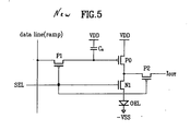
- FIG. 5 is a circuit diagram of a driving circuit in an active matrix method according to the second embodiment of the present invention.
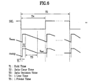
- FIG. 6 is a timing view illustrating each signal waveform according to the second embodiment of the present invention.
- FIG. 7 is a circuit diagram of a driving circuit in an active matrix method according to the third embodiment of the present invention.
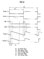
- FIG. 8 is a timing view illustrating each signal waveform according to the third embodiment of the present invention.
- FIG. 9 is a layout illustrating the third embodiment of the present invention.
- FIG. 2 is a circuit diagram of a driving circuit in an active matrix method according to the first embodiment of the present invention
- FIG. 3 is a block diagram illustrating a deviation compensator of the driving circuit according to the present invention.
- the driving circuit includes a transistor P1, a capacitor Cs, a driving transistor PO and a positive power supply VDD.
- the transistor P1 connected data and scan lines switches an externally applied control voltage, and the capacitor Cs stores the control voltage by switching of the transistor P1.
- the driving transistor PO makes an emitting pixel OEL emit lights by the control voltage applied from the capacitor Cs, and the positive power supply VDD supplies a power to the capacitor Cs and the driving transistor PO.
- the driving circuit further includes a switching unit 10 and a deviation compensator 20.
- the switching unit 10 connected between the driving transistor PO and the emitting pixel OEL switches a current applied to the emitting pixel OEL according to a voltage applied from the driving transistor PO.
- the deviation compensator 20 detects the current applied to the emitting pixel OEL by switching of the switching unit 10, and controls the control voltage, so that luminance deviation of the emitting pixel OEL generated from threshold voltage deviation of the driving transistor PO is compensated.
- the switching unit 10 includes a transistor P2 switching the current applied to the emitting pixel OEL by a control signal SEL1, and a transistor P3 switching the current applied to the deviation compensator 20 by a control signal /SEL1.
- the transistors P1, P2 and P3 are PMOS transistors, and are driven by different control signals.
- the transistor P1 is driven by the control signal SEL
- the transistor P2 is driven by the control signal SEL1
- the transistor P3 is driven by the control signal /SEL1.
- the driving transistor PO is connected to the emitting pixel OEL by the transistor P2 unlike the related art in which the driving transistor PO is directly connected to the emitting pixel OEL.
- the deviation compensator 20 for compensating the luminance deviation of the emitting pixel OEL includes a current-to-voltage converter (I-to-V converter) 21, a comparator 22, and a sample & hold circuit (S & H circuit) 23.
- the current-to-voltage converter detects a driving current I out from the transistor P3 and converts the detected driving current to a voltage.
- the comparator 22 compares the voltage converted by the I-to-V converter 21 with a reference voltage Vref that is set to make the emitting pixel OEL emit lights at a predetermined luminance.
- Vref reference voltage
- an external ramp voltage is applied to the sample & hold circuit 23 .
- the sample & hold circuit 23 outputs a certain ramp voltage value to the data line according to result of the comparator 22.
- the sample & hold circuit 23 constantly maintains the ramp voltage Vramp externally input at a point that the converted voltage value is same as the reference voltage value, and outputs the ramp voltage value constantly maintained to the data line.
- the externally input ramp voltage value Vramp is bypassed and is output to the data line.
- FIG. 4 is a timing view illustrating each signal waveform according to the first embodiment of the present invention.
- the transistors P1 and P2 are turned off, simultaneously, the transistor P3 is turned on by the control signal /SEL1.
- the ramp voltage input through the data line drives the driving transistor PO by the transistor P1, and the deviation compensator 20 detects the driving current of the emitting pixel OEL by the transistor P3.
- the detected driving current is converted to the voltage by the current-to-voltage converter 21, and then the converted voltage is compared with the reference voltage by the comparator 22.
- the sample & hold circuit 23 bypasses and continuously outputs the externally input ramp voltage Vramp to the data line until the converted voltage value is same as the reference voltage value.
- the sample & hold circuit 23 constantly maintains the ramp voltage Vramp externally input at a point that the converted voltage value becomes same as the reference voltage value, and outputs the ramp voltage value constantly maintained to the data line.
- the ramp voltage value constantly maintained is continuously output to the data line from a point that the converted voltage value becomes same as the reference voltage value to a point that the converted voltage value is higher than the reference voltage value.
- the ramp voltage value Vramp constantly maintained is higher than the threshold voltage value of the driving transistor that drives the emitting pixel OEL, so that it is possible to solve a problem of the luminance deviation of the emitting pixel OEL according to the threshold voltage deviation of the driving transistor.
- the ramp voltage value Vramp constantly maintained is stored in the capacitor Cs for storing electric charges by the data line.
- the transistors P1 and P2 are turned on, simultaneously, the transistor P3 is turned off by the control signal /SEL1.
- the driving transistor PO of the corresponding emitting pixel OEL is driven by the capacitor Cs for storing the electric charges, and then the emitting pixels OEL emit lights by the driving current applied by the transistor P2 at a constant luminance.
- the deviation compensator of the present invention outputs the ramp voltage value constantly maintained to the data line during a time period 'T1' (hold time), so that it is possible to solve a problem generated by luminance deviation of the emitting pixels OEL according to the threshold voltage deviation of the driving transistors.
- the deviation compensator of the present invention it may be used an amplifier having a high transimpedance value instead of the current-to-voltage converter 21.
- the amplifier having the high transimpedance is used in the present invention, it is possible to obtain desired luminance since a margin of the control voltage according to a level of the driving current can be increased.
- each switching device uses the scan line in common, thereby decreasing an area of the driving circuit, and increasing an emitting area.
- FIG. 5 is a circuit diagram of a driving circuit in an active matrix method according to the second embodiment of the present invention
- FIG. 6 is a timing view illustrating each signal waveform according to the second embodiment of the present invention.
- the second embodiment of the present invention is different to the first embodiment of the present invention in that a driving transistor PO is connected to a NMOS transistor N1, and NMOS transistor N1 and PMOS transistors P1 and P2 are controlled by an equal control signal SEL.
- the NMOS transistor N1 is used, so that it is not required to additionally apply a control signal applied to the transistor N1. That is, since the transistors P1 and P2 are conversely switched, the control signal SEL can control not only the PMOS transistors P1 and P2 but also the NMOS transistor N1.
- the transistors P1 and P2 are respectively turned on, simultaneously, the transistor N1 is turned off.
- a ramp voltage input by a data line drives the driving transistor PO by the transistor P1, and a deviation compensator 20 detects a driving current of an emitting pixel OEL by the transistor P2.
- the deviation compensator 20 outputs the ramp voltage Vramp to the data line by the equal process, and the ramp voltage Vramp is stored in a capacitor Cs for storing electric charges by the data line.
- the transistors P1 and P2 are respectively turned off , simultaneously, the transistor N1 is turned on.
- the driving transistor PO of the corresponding emitting pixel OEL is driven by the capacitor Cs for storing the electric charges, and the emitting pixels OEL emit lights at a constant luminance by the driving current applied by the transistor N1.
- FIG. 7 is a circuit diagram of a driving circuit in an active matrix method according to the third embodiment of the present invention
- FIG. 8 is a timing view illustrating each signal waveform according to the third embodiment of the present invention.
- the third embodiment of the present invention is different to the first embodiment of the present invention in that a NMOS transistor N1 is formed between a node 2 and a node 3, and an amplifier 30 is formed between a transistor P2 and a deviation compensator 20.
- the amplifier 30 amplifies a current applied by the transistor P2, and then input the current to the deviation compensator.
- the amplifier 30 includes NMOS transistors N2 and N3.
- a gate of the NMOS transistor N3 is connected to an output terminal of the transistor P2, and the NMOS transistor N3 outputs the amplified current to the deviation compensator by a voltage difference between gate and source.
- the NMOS transistor N2 is respectively connected to gate and ground of the transistor N3, and controls the voltage difference between the gate and the source of the transistor N2 by an externally applied control signal.
- the embodiment of the present invention includes the amplifier 30 since it is hard to detect a current level of I out in the deviation compensator if the current level of I out is low referring to FIG. 2 and FIG. 5.
- the transistors N2 and N3 are additionally formed to amplify the current level of I out .
- the driving circuit according to the third embodiment of the present invention has the following advantages.
- the NMOS transistor N1 of FIG. 7 uses P-well of the transistors N2 and N3 in common with the transistors N2 and N3, thereby decreasing an area of layout.
- the NMOS transistor N1 of FIG. 7 maintains the node 3 at a voltage higher than -0.7V, thereby preventing the driving transistor PO from being over loaded.
- the driving current of the transistors N2 and N3 in the amplifier makes not only the emitting pixel OEL emit lights, but also an adjacent emitting pixel OEL (not shown) emit lights, thereby decreasing the area of layout referring to FIG. 9.
- a voltage applied to the node 1 during a time period 't3' is determined.
- a process of time period 't4' is repeated as the number of total scan lines during a time period 't5' of FIG. 8.
- FIG. 9 is a layout illustrating FIG. 7.
- the driving transistor PO of FIG. 7 is snake-shaped, so that it is useful to form a device having a long channel within a small pixel, and to enlarge the capacitor Cs of FIG. 7.
- the driving circuit of the active matrix method in the display device according to the present invention has the following advantages.
- the amplifier having the high transimpedance is used in the deviation compensator of the present invention, it is possible to obtain desired luminance since a margin of the control voltage according to the level of the driving current is large.
- the transistor snake-shaped is used in the present invention, thereby decreasing the area of layout. Also, capacitance of the capacitor for storing electric charges can be improved.
Landscapes
- Engineering & Computer Science (AREA)
- Physics & Mathematics (AREA)
- Computer Hardware Design (AREA)
- General Physics & Mathematics (AREA)
- Theoretical Computer Science (AREA)
- Geometry (AREA)
- Microelectronics & Electronic Packaging (AREA)
- Control Of Indicators Other Than Cathode Ray Tubes (AREA)
- Control Of El Displays (AREA)
Description
- This application claims the benefit of the Korean Application No. P2001-00625 filed on January 5, 2001.
- The present invention relates to a driving circuit of an active matrix method in a display device.
- Recently, various display devices such as an LCD device, a PDP device, an FED device and an EL device have been studied with development of flat display devices. These at display devices are classified into two according to a driving method, a passive matrix method and an active matrix method. At this time, it is required to use a higher level of current in the passive matrix method than the active matrix method.
- Accordingly, in current driving methods of the LCD device and the PDP device, since greater current level is required with increasing the number of pixel, the passive matrix method is more efficient.
- Meanwhile, in current driving methods of the FED and EL devices, it is regarded that the active matrix method is more efficient than the passive matrix method since it is required to use the higher level of current in the passive matrix method than the active matrix method even though a line time is equal.
- FIG. 1 is a circuit diagram of a driving circuit according to a related art active matrix method.
- As shown in FIG. 1, the driving circuit includes a scan line SEL, a data line, a switch P1, a capacitor Cs, a driving transistor PO, an OEL and a positive power supply VDD.
- At this time, the scan line SEL selects a pixel for driving, and the data line applies a voltage to the pixel. The switch P1 is served as an active device to control data input according to a signal of the scan line, and the capacitor Cs stores electric charges selected according to the voltage applied to the data line. Next, a voltage is input to the driving transistor PO by the electric charges stored in the capacitor Cs, and then the driving transistor PO applies a current to the OEL. The OEL emits light by the current applied from the driving transistor PO, and the positive power supply VDD supplies a power to the capacitor Cs and the driving transistor PO.
- An operation of an active matrix method in a related art display device will be described in detail.
- First, the pixel driven by the scan line SEL is selected, and then the pixel for driving is turned on by the switch P1. Then, a control voltage, in which a gray is controlled, is applied to the pixel for driving through the data line.
- At this time, the control voltage is stored in the capacitor Cs, simultaneously, drives the driving transistor PO to make the OEL emit lights.
- After the scan line is disabled, the driving transistor PO is driven by the voltage stored in the capacitor Cs to maintain one frame until the next select time.
- However, since threshold voltages of the driving transistors used in the display device are different, the driving current for driving the OEL selected is not constant even though an equal driving voltage is applied to each driving transistor.
- That is, each OEL emits different luminance according to deviation of the threshold voltages of the driving transistors.
- To decrease the luminance deviation of the OEL according to the deviation of the threshold voltages of the driving transistors, it is required to constantly apply the driving current for driving the OEL without regard to the deviation of the threshold voltages of each driving transistor.
- The deviation of the threshold voltages of the driving transistors is necessary consequence in fabricating process steps of the display device. Therefore, the luminance deviation of the pixels has to be compensated by detecting luminance of each pixel, however, it is hard to effectively compensate the luminance deviation.
- Also, in the related art driving circuit, if a margin of the control voltage according to level of the driving current is small, it is hard to obtain desired luminance.
- EP-
A 1 003 150 relates to transistor circuits including driving transistors for controlling a driving current. The variance of voltage/current characteristics and thresholds in driving transistors, leading to variance of driving current to data signals and reducing the precision of the driving current, is discussed. It is proposed to introduce a compensating transistor into the circuit with its gate connected to either its source or drain, and which is connected to the gate of the driving transistor in an orientation so as to supply the input signals to that gate through source and drain of the compensating transistor and to allow the gate of the driving transistor to move electric charge into a direction to lower the conductance. Thus, the compensating transistor has diode characteristics. - WO 99 65012 A discloses an active matrix electroluminescent display with an array of current-driven electroluminescent display elements comprising organic electroluminescent material, whose operations are each controlled by an associated switching means to which a drive signal for determining a desired light output is supplied in a respective address period and which is arranged to drive the display element according to the drive signal following the address period. Each switching means comprises a current mirror circuit which samples and stores the drive signal and comprises a first transistor whose current-carrying electrodes are connected between a supply line and an electrode of the display element, a second transistor to whose gate electrode and first current-carrying electrode the drive signal is applied and whose second current-carrying electrode is connected to the supply line. The gate of the first transistor is connected to the supply line via a storage capacitor and to the gate of the second transistor via a switch device which is operable to connect the gates of the first and second transistors during the address period.
- EP-
A 0 905 673 discloses an active matrix display system with a LED or an OLED pixel structure with five transistors. This structure determines an offset voltage parameter using an autozeroing method which comprises a precharge phase, a auto-zero phase and a data writing phase. The auto-zero phase is essentially a current-drive mode of operation, where the drive current is very small. In the writing phase, the voltage on the LED is incremented above turn-on using the applied data voltage. - Dawson R.M.A. et al., 'The Impact of Transient Response of Organic Light Emitting Diodes on the Design of Active Matrix OLED Displays', Electron Devices Meeting, 1998; IEDM'98 Technical Digest., International San Francisco, CA, USA 6-9 Dec. 1998, Piscataway, NJ, USA, IEEE, US, 6. Dec. 1998, pages 875 - 878, ISBN 0-7803-4774-9, discusses the design of active matrix displays with OLEDs. Circuitries for current and voltage programmed OLED pixels are disclosed. Circuitries (Figs. 7, 9) comprise a first switch or transistor (MN1) connectable to a data line and to a scan line, which is adapted to switch an externally applied control voltage; further a driving unit (C1, MN2), its input being connected to the output of the first switch and adapted to store the control voltage applied by switching of the first switch; and an emitting pixel (OLED), which is connected to the driving unit such that a current is applied to the emitting pixel in dependence of the control voltage being stored in the driving unit.
- It is further disclosed a second switch (MN3), which is adapted for switching a current applied to the emitting pixel by the control voltage applied from the driving unit directly back to the driving unit, without any further compensating circuitry.
- Accordingly, the present invention is directed to a driving circuit of an active matrix method in a display device that substantially obviates one or more problems due to limitations and disadvantages of the related art.
- An object of the present invention is to provide a driving circuit of an active matrix method in a display device that can constantly improve luminance between pixels.
- Additional advantages, objects, and features of the invention will be set forth in part in the description which follows and in part will become apparent to those having ordinary skill in the art upon examination of the following or may be learned from practice of the invention. The objectives and other advantages of the invention may be realized and attained by the structure particularly pointed out in the written description and claims hereof as well as the appended drawings.
- To achieve these objects and other advantages and in accordance with the purpose of the invention, as embodied and broadly described herein, a driving circuit of an active matrix display in a display device according to the present invention comprises a first switch connectable to a data line and to a scan line, adapted to switch an externally applied control voltage; a driving unit, its input being connected to the output of the first switch and adapted to store the control voltage applied by switching of the first switch; an emitting pixel, which is connected to the driving unit such that a current is applied to the emitting pixel in dependence of the control voltage being stored in the driving unit; and further a second switch, adapted for switching a current applied to the emitting pixel by the control voltage applied from the driving unit to a deviation compensator; and the deviation compensator, adapted for detecting the current applied to the emitting pixel and for controlling the control voltage, thereby compensating luminance deviation of the display device according to deviation of the threshold voltages of the driving unit.
- According to an embodiment of the invention, the deviation compensator comprises a converter, adapted for converting the current switched from the second switch to a voltage, a comparator, adapted for comparing the voltage value converted by the converter with a reference voltage value, and a S & H circuit, adapted for receiving an external ramp voltage, and for outputting a certain ramp voltage to the data line according to result of the comparator.
- According to a further embodiment of the invention, the S & H circuit is adapted to output the ramp voltage value constantly maintained to the data line when the converted voltage value is same as or lower than the reference voltage value, and the S & H circuit is adapted to bypass and output the external input ramp voltage value to the data line when the converted voltage value is higher than the reference voltage value.
- According to further alternative embodiments of the invention, the first switch, the first and second transistors are PMOS transistors, and are respectively driven by different control signals, or the first switch and the second transistor are PMOS transistors and the first transistor is an NMOS transistor, the first switch, the first and second transistors being driven by an equal control signal.
- According to a further embodiment, an amplifier formed between the second transistor and the deviation compensator is adapted to amplify the applied current by switching of the second transistor, and to input the amplified current to the deviation comparator.
- According to a further embodiment, the amplifier comprises a third transistor having a gate connected to an output terminal of the second transistor, and is adapted for outputting the current amplified by a voltage difference between gate and source to the deviation compensator, and comprises a fourth transistor connected to gate and ground of the third transistor, and is adapted for controlling the voltage difference by an externally applied control signal.
- It is to be understood that both the foregoing general description and the following detailed description of the present invention are exemplary and explanatory and are intended to provide further explanation of the invention as claimed.
- The accompanying drawings, which are included to provide a further understanding of the invention and are incorporated in and constitute a part of this application, illustrate embodiment(s) of the invention and together with the description serve to explain the principle of the invention. In the drawings:
- FIG. 1 is a circuit diagram of a driving circuit according to a related art active matrix method;
- FIG. 2 is a circuit diagram of a driving circuit in an active matrix method according to the first embodiment of the present invention.
- FIG. 3 is a block diagram illustrating a deviation compensator of a driving circuit according to the present invention;
- FIG. 4 is a timing view illustrating each signal waveform according to the first embodiment of the present invention;
- FIG. 5 is a circuit diagram of a driving circuit in an active matrix method according to the second embodiment of the present invention;
- FIG. 6 is a timing view illustrating each signal waveform according to the second embodiment of the present invention;
- FIG. 7 is a circuit diagram of a driving circuit in an active matrix method according to the third embodiment of the present invention;
- FIG. 8 is a timing view illustrating each signal waveform according to the third embodiment of the present invention; and
- FIG. 9 is a layout illustrating the third embodiment of the present invention.
- Reference will now be made in detail to the preferred embodiments of the present invention, examples of which are illustrated in the accompanying drawings. Wherever possible, the same reference numbers will be used throughout the drawings to refer to the same or like parts.
- FIG. 2 is a circuit diagram of a driving circuit in an active matrix method according to the first embodiment of the present invention, and FIG. 3 is a block diagram illustrating a deviation compensator of the driving circuit according to the present invention.
- As shown in FIG. 2 and FIG. 3, the driving circuit includes a transistor P1, a capacitor Cs, a driving transistor PO and a positive power supply VDD.
- At this time, the transistor P1 connected data and scan lines switches an externally applied control voltage, and the capacitor Cs stores the control voltage by switching of the transistor P1. Next, the driving transistor PO makes an emitting pixel OEL emit lights by the control voltage applied from the capacitor Cs, and the positive power supply VDD supplies a power to the capacitor Cs and the driving transistor PO.
- Also, the driving circuit further includes a
switching unit 10 and adeviation compensator 20. The switchingunit 10 connected between the driving transistor PO and the emitting pixel OEL switches a current applied to the emitting pixel OEL according to a voltage applied from the driving transistor PO. Also, thedeviation compensator 20 detects the current applied to the emitting pixel OEL by switching of the switchingunit 10, and controls the control voltage, so that luminance deviation of the emitting pixel OEL generated from threshold voltage deviation of the driving transistor PO is compensated. - At this time, the switching
unit 10 includes a transistor P2 switching the current applied to the emitting pixel OEL by a control signal SEL1, and a transistor P3 switching the current applied to thedeviation compensator 20 by a control signal /SEL1. - The transistors P1, P2 and P3 are PMOS transistors, and are driven by different control signals.
- That is, the transistor P1 is driven by the control signal SEL, the transistor P2 is driven by the control signal SEL1, and the transistor P3 is driven by the control signal /SEL1.
- As described above, in the present invention, the driving transistor PO is connected to the emitting pixel OEL by the transistor P2 unlike the related art in which the driving transistor PO is directly connected to the emitting pixel OEL.
- As shown in FIG. 3, the
deviation compensator 20 for compensating the luminance deviation of the emitting pixel OEL includes a current-to-voltage converter (I-to-V converter) 21, acomparator 22, and a sample & hold circuit (S & H circuit) 23. The current-to-voltage converter detects a driving current Iout from the transistor P3 and converts the detected driving current to a voltage. Thecomparator 22 compares the voltage converted by the I-to-V converter 21 with a reference voltage Vref that is set to make the emitting pixel OEL emit lights at a predetermined luminance. To the sample & holdcircuit 23, an external ramp voltage is applied. The sample & holdcircuit 23 outputs a certain ramp voltage value to the data line according to result of thecomparator 22. - At this time, the sample & hold
circuit 23 constantly maintains the ramp voltage Vramp externally input at a point that the converted voltage value is same as the reference voltage value, and outputs the ramp voltage value constantly maintained to the data line. - Meanwhile, when the converted voltage value is higher than the reference voltage value, the externally input ramp voltage value Vramp is bypassed and is output to the data line.
- FIG. 4 is a timing view illustrating each signal waveform according to the first embodiment of the present invention.
- As shown in FIG. 4, if the emitting pixel OEL is selected by the control signal SEL, the transistors P1 and P2 are turned off, simultaneously, the transistor P3 is turned on by the control signal /SEL1.
- At this time, the ramp voltage input through the data line drives the driving transistor PO by the transistor P1, and the
deviation compensator 20 detects the driving current of the emitting pixel OEL by the transistor P3. - Referring to FIG. 3, the detected driving current is converted to the voltage by the current-to-
voltage converter 21, and then the converted voltage is compared with the reference voltage by thecomparator 22. - According to result of the
comparator 22, the sample & holdcircuit 23 bypasses and continuously outputs the externally input ramp voltage Vramp to the data line until the converted voltage value is same as the reference voltage value. - If the converted voltage value is same as or lower than the reference voltage value, the sample & hold
circuit 23 constantly maintains the ramp voltage Vramp externally input at a point that the converted voltage value becomes same as the reference voltage value, and outputs the ramp voltage value constantly maintained to the data line. - At this time, the ramp voltage value constantly maintained is continuously output to the data line from a point that the converted voltage value becomes same as the reference voltage value to a point that the converted voltage value is higher than the reference voltage value.
- The ramp voltage value Vramp constantly maintained is higher than the threshold voltage value of the driving transistor that drives the emitting pixel OEL, so that it is possible to solve a problem of the luminance deviation of the emitting pixel OEL according to the threshold voltage deviation of the driving transistor.
- Subsequently, the ramp voltage value Vramp constantly maintained is stored in the capacitor Cs for storing electric charges by the data line.
- Next, if corresponding emitting pixel OEL is selected by the control signal SEL, the transistors P1 and P2 are turned on, simultaneously, the transistor P3 is turned off by the control signal /SEL1.
- Accordingly, the driving transistor PO of the corresponding emitting pixel OEL is driven by the capacitor Cs for storing the electric charges, and then the emitting pixels OEL emit lights by the driving current applied by the transistor P2 at a constant luminance.
- As described above, the deviation compensator of the present invention outputs the ramp voltage value constantly maintained to the data line during a time period 'T1' (hold time), so that it is possible to solve a problem generated by luminance deviation of the emitting pixels OEL according to the threshold voltage deviation of the driving transistors.
- Referring to FIG. 2, in the deviation compensator of the present invention, it may be used an amplifier having a high transimpedance value instead of the current-to-
voltage converter 21. - In the related art driving circuit, if a margin of the control voltage according to a level of the driving current is small, it is hard to obtain desired luminance.
- However, if the amplifier having the high transimpedance is used in the present invention, it is possible to obtain desired luminance since a margin of the control voltage according to a level of the driving current can be increased.
- In another embodiment of the present invention, each switching device uses the scan line in common, thereby decreasing an area of the driving circuit, and increasing an emitting area.
- FIG. 5 is a circuit diagram of a driving circuit in an active matrix method according to the second embodiment of the present invention, and FIG. 6 is a timing view illustrating each signal waveform according to the second embodiment of the present invention.
- As shown in FIG. 5, the second embodiment of the present invention is different to the first embodiment of the present invention in that a driving transistor PO is connected to a NMOS transistor N1, and NMOS transistor N1 and PMOS transistors P1 and P2 are controlled by an equal control signal SEL.
- In the second embodiment of the present invention, the NMOS transistor N1 is used, so that it is not required to additionally apply a control signal applied to the transistor N1. That is, since the transistors P1 and P2 are conversely switched, the control signal SEL can control not only the PMOS transistors P1 and P2 but also the NMOS transistor N1.
- Referring to FIG. 5 and FIG. 6, an operation of the driving circuit will be described in detail.
- If corresponding emitting pixel OEL is selected by the control signal SEL, the transistors P1 and P2 are respectively turned on, simultaneously, the transistor N1 is turned off.
- At this time, a ramp voltage input by a data line drives the driving transistor PO by the transistor P1, and a
deviation compensator 20 detects a driving current of an emitting pixel OEL by the transistor P2. - Referring to FIG. 3 and FIG. 4, the
deviation compensator 20 outputs the ramp voltage Vramp to the data line by the equal process, and the ramp voltage Vramp is stored in a capacitor Cs for storing electric charges by the data line. - Next, if the corresponding emitting pixel OEL is selected by the control signal SEL, the transistors P1 and P2 are respectively turned off , simultaneously, the transistor N1 is turned on.
- Then, the driving transistor PO of the corresponding emitting pixel OEL is driven by the capacitor Cs for storing the electric charges, and the emitting pixels OEL emit lights at a constant luminance by the driving current applied by the transistor N1.
- The other embodiment of the present invention will be described with reference to the accompanying drawings.
- FIG. 7 is a circuit diagram of a driving circuit in an active matrix method according to the third embodiment of the present invention, and FIG. 8 is a timing view illustrating each signal waveform according to the third embodiment of the present invention.
- Referring to FIG. 7, the third embodiment of the present invention is different to the first embodiment of the present invention in that a NMOS transistor N1 is formed between a
node 2 and a node 3, and anamplifier 30 is formed between a transistor P2 and adeviation compensator 20. - At this time, the
amplifier 30 amplifies a current applied by the transistor P2, and then input the current to the deviation compensator. - The
amplifier 30 includes NMOS transistors N2 and N3. - A gate of the NMOS transistor N3 is connected to an output terminal of the transistor P2, and the NMOS transistor N3 outputs the amplified current to the deviation compensator by a voltage difference between gate and source.
- The NMOS transistor N2 is respectively connected to gate and ground of the transistor N3, and controls the voltage difference between the gate and the source of the transistor N2 by an externally applied control signal.
- The embodiment of the present invention includes the
amplifier 30 since it is hard to detect a current level of Iout in the deviation compensator if the current level of Iout is low referring to FIG. 2 and FIG. 5. - Accordingly, in the third embodiment of the present invention, the transistors N2 and N3 are additionally formed to amplify the current level of Iout.
- As shown in FIG. 7, if the electric charges are stored in parasitic capacitance of a node 4, and Vgs (voltage between the gate and source) of the transistor N3 is increased, the amplified Iout is output.
- The driving circuit according to the third embodiment of the present invention has the following advantages.
- First, the NMOS transistor N1 of FIG. 7 uses P-well of the transistors N2 and N3 in common with the transistors N2 and N3, thereby decreasing an area of layout.
- Next, in case that a negative voltage is applied to the node 3, the NMOS transistor N1 of FIG. 7 maintains the node 3 at a voltage higher than -0.7V, thereby preventing the driving transistor PO from being over loaded.
- Also, the driving current of the transistors N2 and N3 in the amplifier makes not only the emitting pixel OEL emit lights, but also an adjacent emitting pixel OEL (not shown) emit lights, thereby decreasing the area of layout referring to FIG. 9.
- As shown in FIG. 7 and FIG. 8, an operation of the third embodiment of the present invention will be described as follows.
- When the scan signal of FIG. 7 is applied during a time period 't4' of FIG. 8 that is called as one scan time, the transistors P1 and P2 respectively are turned on, and the transistor N1 is turned off.
- During a time period 't1' of FIG. 8, a column line to which Iout is output is cleared, and data in a
node 1 is cleared by Vramp signal during a time period 't2'. - Also, a voltage applied to the
node 1 during a time period 't3' is determined. - A process of time period 't4' is repeated as the number of total scan lines during a time period 't5' of FIG. 8.
- FIG. 9 is a layout illustrating FIG. 7.
- As shown in FIG. 9, the driving transistor PO of FIG. 7 is snake-shaped, so that it is useful to form a device having a long channel within a small pixel, and to enlarge the capacitor Cs of FIG. 7.
- As described above, the driving circuit of the active matrix method in the display device according to the present invention has the following advantages.
- First, it is possible to decrease the luminance deviation of the emitting pixels without regard to the deviation of the threshold voltages of the driving transistors, thereby improving uniformity of the luminance.
- Furthermore, if the amplifier having the high transimpedance is used in the deviation compensator of the present invention, it is possible to obtain desired luminance since a margin of the control voltage according to the level of the driving current is large.
- Finally, the transistor snake-shaped is used in the present invention, thereby decreasing the area of layout. Also, capacitance of the capacitor for storing electric charges can be improved.
- It will be apparent to those skilled in the art than various modifications and variations can be made in the present invention. Thus, it is intended that the present invention covers the modifications and variations of this invention provided they come within the scope of the appended claims.
Claims (16)
- A driving circuit of an active matrix display in a display device comprising:a first switch (P1) connectable to a data line and to a scan line (SEL), adapted to switch an externally applied control voltage;a driving unit (Cs, P0), its input being connected to the output of the first switch and adapted to store the control voltage applied by switching of the first switch (P1);an emitting pixel (OEL), which is connected to the driving unit (Cs, PO) such that a current is applied to the emitting pixel (OEL) in dependence of the control voltage being stored in the driving unit (Cs, PO);
characterized bya second switch (10), adapted for switching a current applied to the emitting pixel (OEL) by the control voltage applied from the driving unit to a deviation compensator (20); andthe deviation compensator (20), adapted for detecting the current applied to the emitting pixel (OEL) and for controlling the control voltage, thereby compensating luminance deviation of the display device according to deviation of the threshold voltages of the driving unit. - The driving circuit as claimed in claim 1,
characterized in that
the deviation compensator (20) comprises:a converter (21), adapted for converting the current switched from the second switch (10) to a voltage,a comparator (22), adapted for comparing the voltage value converted by the converter (21) with a reference voltage value (Vref), anda S & H circuit (23), adapted for receiving an external ramp voltage (Vramp), and for outputting a certain ramp voltage (ramp) to the data line according to result of the comparator (22). - The driving circuit as claimed in claim 2,
characterized in that
the S & H circuit (23) is adapted to output the ramp voltage value (ramp) constantly maintained to the data line when the converted voltage value is same as or lower than the reference voltage value (Vref), and the S & H circuit (23) is adapted to bypass and output the external input ramp voltage value (Vramp) to the data line when the converted voltage value is higher than the reference voltage value (Vref). - The driving circuit as claimed in claim 1,
characterized in that
the deviation compensator (20) comprises:a transimpedance amplifier (30), adapted for converting the current switched from the second switch to a voltage amplified,a comparator (22), adapted for comparing the voltage converted by the transimpedance amplifier (30) with a reference voltage (Vref), anda S & H circuit (23), adapted for receiving an external ramp voltage (Vramp) and for outputting a certain ramp voltage (ramp) to the data line according to result of the comparator (22). - The driving circuit as claimed in claim 4,
characterized in that
the S & H circuit (23) is adapted to output the ramp voltage value (ramp) constantly maintained to the data line when the converted voltage value is same as or lower than the reference voltage value (Vref), and the S & H circuit (23) is adapted to bypass and output the externally input ramp voltage value (Vramp) to the data line when the converted voltage value is higher than the reference voltage value (Vref). - The driving circuit as claimed in one of the preceding claims,
characterized in that
the second switch (10) comprises:a first transistor (P2) formed between the driving unit (Cs, PO) and the emitting pixel (OEL), adapted to switch the current applied to the emitting pixel (OEL), anda second transistor (P3) formed between the driving unit (Cs, PO) and the deviation compensator (20), adapted to switch the current applied to the deviation compensator (20). - The driving circuit as claimed in claim 6,
characterized in that
the first and second transistors (P2, P3) are PMOS transistors, and are driven by different control signals (SEL1, /SEL1). - The driving circuit as claimed in claim 6,
characterized in that
the first transistor is NMOS transistor (N1), and the second transistor is PMOS transistor (P2), the first and second transistors driven by an equal control signal (SEL). - The driving circuit as claimed in one of the preceding claims,
characterized by
an amplifier (30) formed between the second switch (10) and the deviation compensator (20), adapted to amplify the applied current by switching of the second switch (10), and to input the amplified current to the deviation compensator (20). - The driving circuit as claimed in claim 9,
characterized in that
the amplifier (30) comprises:a third transistor (N3) having a gate connected to an output terminal of the second switch, and adapted for outputting the current amplified by a voltage difference between gate and source to the deviation compensator (20), anda fourth transistor (N2) connected to gate and ground of the third transistor (N3), and adapted for controlling the voltage difference by an externally applied control signal (RS). - The driving circuit as claimed in claim 10,
characterized in that
the third and fourth transistors are NMOS transistors (N2, N3). - The driving circuit as claimed in claim 6,
characterized in that
the first switch, the first and second transistors are PMOS transistors, and are respectively driven by different control signals. - The driving circuit as claimed in claim 6,
characterized in that
the first switch and the second transistor are PMOS transistors and the first transistor is an NMOS transistor, the first switch, the first and second transistors being driven by an equal control signal. - The driving circuit as claimed in one of claims 6 to 13,
characterized by
an amplifier formed between the second transistor and the deviation compensator adapted to amplify the applied current by switching of the second transistor, and to input the amplified current to the deviation comparator. - The driving circuit as claimed in claim 14,
characterized in that
the amplifier comprises:a third transistor having a gate connected to an output terminal of the second transistor, and adapted for outputting the current amplified by a voltage difference between gate and source to the deviation compensator, anda fourth transistor connected to gate and ground of the third transistor, and adapted for controlling the voltage difference by an externally applied control signal. - The driving circuit as claimed in claim 15,
characterized in that
the third and fourth transistors are NMOS transistors.
Applications Claiming Priority (2)
| Application Number | Priority Date | Filing Date | Title |
|---|---|---|---|
| KR10-2001-0000625A KR100370095B1 (en) | 2001-01-05 | 2001-01-05 | Drive Circuit of Active Matrix Formula for Display Device |
| KR2001000625 | 2001-01-05 |
Publications (3)
| Publication Number | Publication Date |
|---|---|
| EP1221686A2 EP1221686A2 (en) | 2002-07-10 |
| EP1221686A3 EP1221686A3 (en) | 2003-03-19 |
| EP1221686B1 true EP1221686B1 (en) | 2007-03-14 |
Family
ID=19704305
Family Applications (1)
| Application Number | Title | Priority Date | Filing Date |
|---|---|---|---|
| EP02000314A Expired - Lifetime EP1221686B1 (en) | 2001-01-05 | 2002-01-03 | Driving circuit of an active matrix display with compensation of threshold voltage deviation |
Country Status (5)
| Country | Link |
|---|---|
| US (1) | US6917350B2 (en) |
| EP (1) | EP1221686B1 (en) |
| KR (1) | KR100370095B1 (en) |
| CN (1) | CN1180389C (en) |
| DE (1) | DE60218762T2 (en) |
Cited By (1)
| Publication number | Priority date | Publication date | Assignee | Title |
|---|---|---|---|---|
| CN101253574B (en) * | 2005-07-01 | 2012-08-22 | 剑桥模拟技术股份有限公司 | Sampled-data circuits using zero crossing detection |
Families Citing this family (52)
| Publication number | Priority date | Publication date | Assignee | Title |
|---|---|---|---|---|
| JP4498669B2 (en) | 2001-10-30 | 2010-07-07 | 株式会社半導体エネルギー研究所 | Semiconductor device, display device, and electronic device including the same |
| JP2004054238A (en) * | 2002-05-31 | 2004-02-19 | Seiko Epson Corp | Electronic circuit, electro-optical device, method of driving electro-optical device, and electronic apparatus |
| KR100445097B1 (en) * | 2002-07-24 | 2004-08-21 | 주식회사 하이닉스반도체 | Flat panel display device for compensating threshold voltage of panel |
| US7002302B2 (en) | 2002-10-07 | 2006-02-21 | Samsung Sdi Co., Ltd. | Flat panel display |
| GB0223305D0 (en) * | 2002-10-08 | 2002-11-13 | Koninkl Philips Electronics Nv | Electroluminescent display devices |
| US7612749B2 (en) * | 2003-03-04 | 2009-11-03 | Chi Mei Optoelectronics Corporation | Driving circuits for displays |
| JP4049010B2 (en) * | 2003-04-30 | 2008-02-20 | ソニー株式会社 | Display device |
| JP3772889B2 (en) * | 2003-05-19 | 2006-05-10 | セイコーエプソン株式会社 | Electro-optical device and driving device thereof |
| GB0320503D0 (en) * | 2003-09-02 | 2003-10-01 | Koninkl Philips Electronics Nv | Active maxtrix display devices |
| KR100514183B1 (en) * | 2003-09-08 | 2005-09-13 | 삼성에스디아이 주식회사 | Pixel driving circuit and method for organic electroluminescent display |
| KR100599726B1 (en) * | 2003-11-27 | 2006-07-12 | 삼성에스디아이 주식회사 | Light emitting display device, display panel and driving method thereof |
| JP4297438B2 (en) * | 2003-11-24 | 2009-07-15 | 三星モバイルディスプレイ株式會社 | Light emitting display device, display panel, and driving method of light emitting display device |
| GB0328584D0 (en) | 2003-12-10 | 2004-01-14 | Koninkl Philips Electronics Nv | Video data signal correction |
| CN1898719B (en) * | 2003-12-23 | 2010-04-21 | 汤姆森特许公司 | Apparatus for displaying images on an active matrix |
| DE10360816A1 (en) * | 2003-12-23 | 2005-07-28 | Deutsche Thomson-Brandt Gmbh | Circuit and driving method for a light-emitting display |
| EP1700290B1 (en) * | 2003-12-31 | 2019-01-16 | Thomson Licensing | Image display screen and method of addressing said screen |
| DE102004022424A1 (en) * | 2004-05-06 | 2005-12-01 | Deutsche Thomson-Brandt Gmbh | Circuit and driving method for a light-emitting display |
| CA2472671A1 (en) * | 2004-06-29 | 2005-12-29 | Ignis Innovation Inc. | Voltage-programming scheme for current-driven amoled displays |
| KR100624318B1 (en) * | 2004-12-24 | 2006-09-19 | 삼성에스디아이 주식회사 | Data integrated circuit, light emitting display using same and driving method thereof |
| KR100700846B1 (en) * | 2004-12-24 | 2007-03-27 | 삼성에스디아이 주식회사 | Data integrated circuit and light emitting display device using the same |
| KR100604066B1 (en) * | 2004-12-24 | 2006-07-24 | 삼성에스디아이 주식회사 | Pixel and light emitting display device using same |
| KR100611914B1 (en) | 2004-12-24 | 2006-08-11 | 삼성에스디아이 주식회사 | Data integrated circuit, light emitting display using same and driving method thereof |
| KR100613091B1 (en) * | 2004-12-24 | 2006-08-16 | 삼성에스디아이 주식회사 | Data integrated circuit, light emitting display using same and driving method thereof |
| KR100613088B1 (en) * | 2004-12-24 | 2006-08-16 | 삼성에스디아이 주식회사 | Data integrated circuit and light emitting display device using the same |
| US7459942B2 (en) * | 2005-07-01 | 2008-12-02 | Cambridge Analog Technologies, Inc. | Sampled-data circuits using zero crossing detection |
| KR100768047B1 (en) * | 2005-11-30 | 2007-10-18 | 엘지.필립스 엘시디 주식회사 | Organic light emitting diode display device and driving method thereof |
| EP1796070A1 (en) | 2005-12-08 | 2007-06-13 | Thomson Licensing | Luminous display and method for controlling the same |
| US7504866B2 (en) | 2005-12-29 | 2009-03-17 | Cambridge Analog Technologies, Inc. | Output hold circuits for sample-data circuits |
| US7522086B2 (en) | 2005-12-29 | 2009-04-21 | Cambridge Analog Technologies, Inc. | Reference circuits for sampled-data circuits |
| KR101226814B1 (en) * | 2006-02-15 | 2013-01-25 | 프리즘, 인코포레이티드 | Servo-assisted scanning beam display systems having screens with on-screen reference marks |
| KR100671669B1 (en) * | 2006-02-28 | 2007-01-19 | 삼성에스디아이 주식회사 | Data driver, organic light emitting display using same and driving method thereof |
| KR100967142B1 (en) * | 2006-08-01 | 2010-07-06 | 가시오게산키 가부시키가이샤 | Display drive device and display device |
| JP5240538B2 (en) * | 2006-11-15 | 2013-07-17 | カシオ計算機株式会社 | Display driving device and driving method thereof, and display device and driving method thereof |
| KR101416904B1 (en) * | 2007-11-07 | 2014-07-09 | 엘지디스플레이 주식회사 | Driving apparatus for organic electro-luminescence display device |
| US20090167644A1 (en) * | 2007-12-28 | 2009-07-02 | White Christopher J | Resetting drive transistors in electronic displays |
| JP5157791B2 (en) * | 2008-09-29 | 2013-03-06 | カシオ計算機株式会社 | Display drive device, display device, and drive control method for display device |
| TWI416467B (en) | 2009-09-08 | 2013-11-21 | Au Optronics Corp | Active matrix organic light emitting diode (oled) display, pixel circuit and data current writing method thereof |
| JP5146521B2 (en) * | 2009-12-28 | 2013-02-20 | カシオ計算機株式会社 | Pixel drive device, light emitting device, drive control method thereof, and electronic apparatus |
| JP5240581B2 (en) * | 2009-12-28 | 2013-07-17 | カシオ計算機株式会社 | Pixel drive device, light emitting device, drive control method thereof, and electronic apparatus |
| JP5955073B2 (en) | 2012-04-23 | 2016-07-20 | キヤノン株式会社 | Display device and driving method of display device |
| US9747834B2 (en) * | 2012-05-11 | 2017-08-29 | Ignis Innovation Inc. | Pixel circuits including feedback capacitors and reset capacitors, and display systems therefore |
| CN105164743B (en) * | 2013-03-15 | 2018-05-25 | 夏普株式会社 | Active matrix substrate, method of manufacturing active matrix substrate, and display panel |
| KR102083458B1 (en) * | 2013-12-26 | 2020-03-02 | 엘지디스플레이 주식회사 | Organic Light Emitting Display and Image Quality Compensation Method Of The Same |
| CN104506172B (en) * | 2014-11-26 | 2017-03-15 | 四川长虹欣锐科技有限公司 | A kind of 4 20mA current loop control PWM output circuits |
| KR102577493B1 (en) * | 2016-07-29 | 2023-09-11 | 엘지디스플레이 주식회사 | Organic light emitting device and its driving method |
| KR102636682B1 (en) * | 2016-12-21 | 2024-02-15 | 엘지디스플레이 주식회사 | Display device and driving method therof |
| CN107016965B (en) * | 2017-05-26 | 2019-04-30 | 深圳市华星光电半导体显示技术有限公司 | Compensation method and pixel driving circuit for OVSS voltage drop of OLED display device |
| CN109147669B (en) * | 2017-06-15 | 2020-04-10 | 京东方科技集团股份有限公司 | Pixel circuit, driving method thereof and display panel |
| US11710445B2 (en) * | 2019-01-24 | 2023-07-25 | Google Llc | Backplane configurations and operations |
| JP2021117369A (en) | 2020-01-27 | 2021-08-10 | ソニーセミコンダクタソリューションズ株式会社 | Display device |
| WO2021184192A1 (en) * | 2020-03-17 | 2021-09-23 | 京东方科技集团股份有限公司 | Pixel circuit and driving method therefor, and display apparatus |
| CN116682359B (en) * | 2022-02-22 | 2026-04-07 | 成都辰显光电有限公司 | Pixel circuit driving method and display device |
Family Cites Families (14)
| Publication number | Priority date | Publication date | Assignee | Title |
|---|---|---|---|---|
| JPS5957288A (en) * | 1982-09-27 | 1984-04-02 | シチズン時計株式会社 | Driving of matrix display |
| JP2792791B2 (en) | 1992-08-20 | 1998-09-03 | シャープ株式会社 | Display device |
| US5701136A (en) * | 1995-03-06 | 1997-12-23 | Thomson Consumer Electronics S.A. | Liquid crystal display driver with threshold voltage drift compensation |
| US5952789A (en) * | 1997-04-14 | 1999-09-14 | Sarnoff Corporation | Active matrix organic light emitting diode (amoled) display pixel structure and data load/illuminate circuit therefor |
| US6229506B1 (en) * | 1997-04-23 | 2001-05-08 | Sarnoff Corporation | Active matrix light emitting diode pixel structure and concomitant method |
| JP3767877B2 (en) | 1997-09-29 | 2006-04-19 | 三菱化学株式会社 | Active matrix light emitting diode pixel structure and method thereof |
| JP3629939B2 (en) * | 1998-03-18 | 2005-03-16 | セイコーエプソン株式会社 | Transistor circuit, display panel and electronic device |
| GB9812739D0 (en) * | 1998-06-12 | 1998-08-12 | Koninkl Philips Electronics Nv | Active matrix electroluminescent display devices |
| US6384804B1 (en) * | 1998-11-25 | 2002-05-07 | Lucent Techonologies Inc. | Display comprising organic smart pixels |
| JP4505868B2 (en) | 1999-03-12 | 2010-07-21 | 双葉電子工業株式会社 | Luminance compensation circuit for field emission display device |
| US6501449B1 (en) * | 1999-12-08 | 2002-12-31 | Industrial Technology Research Institute | High matching precision OLED driver by using a current-cascaded method |
| US6307322B1 (en) * | 1999-12-28 | 2001-10-23 | Sarnoff Corporation | Thin-film transistor circuitry with reduced sensitivity to variance in transistor threshold voltage |
| KR100348274B1 (en) * | 2000-07-20 | 2002-08-09 | 엘지전자 주식회사 | Circuit of Active Device Drive and Control Method for the same |
| KR20020027957A (en) * | 2000-10-06 | 2002-04-15 | 구자홍 | drive circuit for current driving of active matrix formula |
-
2001
- 2001-01-05 KR KR10-2001-0000625A patent/KR100370095B1/en not_active Expired - Lifetime
-
2002
- 2002-01-03 US US10/033,979 patent/US6917350B2/en not_active Expired - Lifetime
- 2002-01-03 DE DE60218762T patent/DE60218762T2/en not_active Expired - Lifetime
- 2002-01-03 EP EP02000314A patent/EP1221686B1/en not_active Expired - Lifetime
- 2002-01-05 CN CNB021031967A patent/CN1180389C/en not_active Expired - Lifetime
Cited By (1)
| Publication number | Priority date | Publication date | Assignee | Title |
|---|---|---|---|---|
| CN101253574B (en) * | 2005-07-01 | 2012-08-22 | 剑桥模拟技术股份有限公司 | Sampled-data circuits using zero crossing detection |
Also Published As
| Publication number | Publication date |
|---|---|
| US6917350B2 (en) | 2005-07-12 |
| EP1221686A2 (en) | 2002-07-10 |
| EP1221686A3 (en) | 2003-03-19 |
| KR20020057538A (en) | 2002-07-11 |
| CN1180389C (en) | 2004-12-15 |
| KR100370095B1 (en) | 2003-02-05 |
| CN1363916A (en) | 2002-08-14 |
| DE60218762T2 (en) | 2007-12-06 |
| DE60218762D1 (en) | 2007-04-26 |
| US20020089357A1 (en) | 2002-07-11 |
Similar Documents
| Publication | Publication Date | Title |
|---|---|---|
| US6917350B2 (en) | Driving circuit of active matrix method in display device | |
| KR100497247B1 (en) | Light emitting display device and display panel and driving method thereof | |
| US9424770B2 (en) | Error compensator and organic light emitting display device using the same | |
| US7236149B2 (en) | Pixel circuit, display device, and driving method of pixel circuit | |
| US9336713B2 (en) | Organic light emitting display and driving method thereof | |
| US10019941B2 (en) | Compensation technique for luminance degradation in electro-luminance devices | |
| US8120556B2 (en) | Organic light emitting display having longer life span | |
| JP4062179B2 (en) | Pixel circuit, display device, and driving method of pixel circuit | |
| US11308877B2 (en) | Display driving device and display device including the same | |
| US7825881B2 (en) | Organic light emitting display device | |
| US20150130780A1 (en) | Organic light emitting display and driving method thereof | |
| CN109686318B (en) | Pixel driving circuit and driving method | |
| US20060022204A1 (en) | Electroluminescent display devices | |
| US20110148847A1 (en) | Method of driving display apparatus | |
| KR102627269B1 (en) | Organic Light Emitting Display having a Compensation Circuit for Driving Characteristic | |
| CN100378781C (en) | Display panel and driving method thereof | |
| US20060124944A1 (en) | Pixel circuit and light emitting display using the same | |
| GB2360870A (en) | Driver circuit for organic electroluminescent device | |
| US6847171B2 (en) | Organic electroluminescent device compensated pixel driver circuit | |
| US20050110725A1 (en) | Flat panel display device with triodic rectifier switch | |
| KR102618603B1 (en) | Organic Light Emitting Display Device | |
| KR100536237B1 (en) | Light emitting display device and driving method thereof | |
| KR20220161036A (en) | Electroluminescence Display Device And Driving Method Of The Same | |
| KR101390316B1 (en) | AMOLED and driving method thereof | |
| JP4581337B2 (en) | Pixel circuit, display device, and driving method of pixel circuit |
Legal Events
| Date | Code | Title | Description |
|---|---|---|---|
| PUAI | Public reference made under article 153(3) epc to a published international application that has entered the european phase |
Free format text: ORIGINAL CODE: 0009012 |
|
| AK | Designated contracting states |
Kind code of ref document: A2 Designated state(s): AT BE CH CY DE DK ES FI FR GB GR IE IT LI LU MC NL PT SE TR |
|
| AX | Request for extension of the european patent |
Free format text: AL;LT;LV;MK;RO;SI |
|
| PUAL | Search report despatched |
Free format text: ORIGINAL CODE: 0009013 |
|
| AK | Designated contracting states |
Kind code of ref document: A3 Designated state(s): AT BE CH CY DE DK ES FI FR GB GR IE IT LI LU MC NL PT SE TR Designated state(s): AT BE CH CY DE DK ES FI FR GB GR IE IT LI LU MC NL PT SE TR |
|
| AX | Request for extension of the european patent |
Extension state: AL LT LV MK RO SI |
|
| 17P | Request for examination filed |
Effective date: 20030918 |
|
| 17Q | First examination report despatched |
Effective date: 20031016 |
|
| AKX | Designation fees paid |
Designated state(s): DE FR GB NL |
|
| RTI1 | Title (correction) |
Free format text: DRIVING CIRCUIT OF AN ACTIVE MATRIX DISPLAY WITH COMPENSATION OF THRESHOLD VOLTAGE DEVIATION |
|
| GRAP | Despatch of communication of intention to grant a patent |
Free format text: ORIGINAL CODE: EPIDOSNIGR1 |
|
| GRAS | Grant fee paid |
Free format text: ORIGINAL CODE: EPIDOSNIGR3 |
|
| GRAA | (expected) grant |
Free format text: ORIGINAL CODE: 0009210 |
|
| AK | Designated contracting states |
Kind code of ref document: B1 Designated state(s): DE FR GB NL |
|
| REG | Reference to a national code |
Ref country code: GB Ref legal event code: FG4D |
|
| REF | Corresponds to: |
Ref document number: 60218762 Country of ref document: DE Date of ref document: 20070426 Kind code of ref document: P |
|
| ET | Fr: translation filed | ||
| PLBE | No opposition filed within time limit |
Free format text: ORIGINAL CODE: 0009261 |
|
| STAA | Information on the status of an ep patent application or granted ep patent |
Free format text: STATUS: NO OPPOSITION FILED WITHIN TIME LIMIT |
|
| 26N | No opposition filed |
Effective date: 20071217 |
|
| REG | Reference to a national code |
Ref country code: GB Ref legal event code: 732E |
|
| NLS | Nl: assignments of ep-patents |
Owner name: LG DISPLAY CO., LTD. Effective date: 20080530 |
|
| REG | Reference to a national code |
Ref country code: FR Ref legal event code: TP |
|
| REG | Reference to a national code |
Ref country code: FR Ref legal event code: PLFP Year of fee payment: 15 |
|
| REG | Reference to a national code |
Ref country code: FR Ref legal event code: PLFP Year of fee payment: 16 |
|
| REG | Reference to a national code |
Ref country code: FR Ref legal event code: PLFP Year of fee payment: 17 |
|
| PGFP | Annual fee paid to national office [announced via postgrant information from national office to epo] |
Ref country code: FR Payment date: 20201204 Year of fee payment: 20 Ref country code: GB Payment date: 20201130 Year of fee payment: 20 |
|
| PGFP | Annual fee paid to national office [announced via postgrant information from national office to epo] |
Ref country code: NL Payment date: 20201208 Year of fee payment: 20 |
|
| PGFP | Annual fee paid to national office [announced via postgrant information from national office to epo] |
Ref country code: DE Payment date: 20201125 Year of fee payment: 20 |
|
| REG | Reference to a national code |
Ref country code: DE Ref legal event code: R071 Ref document number: 60218762 Country of ref document: DE |
|
| REG | Reference to a national code |
Ref country code: NL Ref legal event code: MK Effective date: 20220102 |
|
| REG | Reference to a national code |
Ref country code: GB Ref legal event code: PE20 Expiry date: 20220102 |
|
| PG25 | Lapsed in a contracting state [announced via postgrant information from national office to epo] |
Ref country code: GB Free format text: LAPSE BECAUSE OF EXPIRATION OF PROTECTION Effective date: 20220102 |