EP1220018A1 - Liquid crystal display panel and method for manufacturing the same, and liquid crystal display - Google Patents
Liquid crystal display panel and method for manufacturing the same, and liquid crystal display Download PDFInfo
- Publication number
- EP1220018A1 EP1220018A1 EP01954377A EP01954377A EP1220018A1 EP 1220018 A1 EP1220018 A1 EP 1220018A1 EP 01954377 A EP01954377 A EP 01954377A EP 01954377 A EP01954377 A EP 01954377A EP 1220018 A1 EP1220018 A1 EP 1220018A1
- Authority
- EP
- European Patent Office
- Prior art keywords
- liquid crystal
- crystal display
- drive circuit
- display panel
- circuit
- Prior art date
- Legal status (The legal status is an assumption and is not a legal conclusion. Google has not performed a legal analysis and makes no representation as to the accuracy of the status listed.)
- Ceased
Links
Images




Classifications
-
- G—PHYSICS
- G02—OPTICS
- G02F—OPTICAL DEVICES OR ARRANGEMENTS FOR THE CONTROL OF LIGHT BY MODIFICATION OF THE OPTICAL PROPERTIES OF THE MEDIA OF THE ELEMENTS INVOLVED THEREIN; NON-LINEAR OPTICS; FREQUENCY-CHANGING OF LIGHT; OPTICAL LOGIC ELEMENTS; OPTICAL ANALOGUE/DIGITAL CONVERTERS
- G02F1/00—Devices or arrangements for the control of the intensity, colour, phase, polarisation or direction of light arriving from an independent light source, e.g. switching, gating or modulating; Non-linear optics
- G02F1/01—Devices or arrangements for the control of the intensity, colour, phase, polarisation or direction of light arriving from an independent light source, e.g. switching, gating or modulating; Non-linear optics for the control of the intensity, phase, polarisation or colour
- G02F1/13—Devices or arrangements for the control of the intensity, colour, phase, polarisation or direction of light arriving from an independent light source, e.g. switching, gating or modulating; Non-linear optics for the control of the intensity, phase, polarisation or colour based on liquid crystals, e.g. single liquid crystal display cells
- G02F1/133—Constructional arrangements; Operation of liquid crystal cells; Circuit arrangements
-
- G—PHYSICS
- G09—EDUCATION; CRYPTOGRAPHY; DISPLAY; ADVERTISING; SEALS
- G09G—ARRANGEMENTS OR CIRCUITS FOR CONTROL OF INDICATING DEVICES USING STATIC MEANS TO PRESENT VARIABLE INFORMATION
- G09G3/00—Control arrangements or circuits, of interest only in connection with visual indicators other than cathode-ray tubes
- G09G3/006—Electronic inspection or testing of displays and display drivers, e.g. of LED or LCD displays
-
- G—PHYSICS
- G02—OPTICS
- G02F—OPTICAL DEVICES OR ARRANGEMENTS FOR THE CONTROL OF LIGHT BY MODIFICATION OF THE OPTICAL PROPERTIES OF THE MEDIA OF THE ELEMENTS INVOLVED THEREIN; NON-LINEAR OPTICS; FREQUENCY-CHANGING OF LIGHT; OPTICAL LOGIC ELEMENTS; OPTICAL ANALOGUE/DIGITAL CONVERTERS
- G02F1/00—Devices or arrangements for the control of the intensity, colour, phase, polarisation or direction of light arriving from an independent light source, e.g. switching, gating or modulating; Non-linear optics
- G02F1/01—Devices or arrangements for the control of the intensity, colour, phase, polarisation or direction of light arriving from an independent light source, e.g. switching, gating or modulating; Non-linear optics for the control of the intensity, phase, polarisation or colour
- G02F1/13—Devices or arrangements for the control of the intensity, colour, phase, polarisation or direction of light arriving from an independent light source, e.g. switching, gating or modulating; Non-linear optics for the control of the intensity, phase, polarisation or colour based on liquid crystals, e.g. single liquid crystal display cells
- G02F1/133—Constructional arrangements; Operation of liquid crystal cells; Circuit arrangements
- G02F1/1333—Constructional arrangements; Manufacturing methods
- G02F1/1345—Conductors connecting electrodes to cell terminals
- G02F1/13452—Conductors connecting driver circuitry and terminals of panels
-
- G—PHYSICS
- G02—OPTICS
- G02F—OPTICAL DEVICES OR ARRANGEMENTS FOR THE CONTROL OF LIGHT BY MODIFICATION OF THE OPTICAL PROPERTIES OF THE MEDIA OF THE ELEMENTS INVOLVED THEREIN; NON-LINEAR OPTICS; FREQUENCY-CHANGING OF LIGHT; OPTICAL LOGIC ELEMENTS; OPTICAL ANALOGUE/DIGITAL CONVERTERS
- G02F1/00—Devices or arrangements for the control of the intensity, colour, phase, polarisation or direction of light arriving from an independent light source, e.g. switching, gating or modulating; Non-linear optics
- G02F1/01—Devices or arrangements for the control of the intensity, colour, phase, polarisation or direction of light arriving from an independent light source, e.g. switching, gating or modulating; Non-linear optics for the control of the intensity, phase, polarisation or colour
- G02F1/13—Devices or arrangements for the control of the intensity, colour, phase, polarisation or direction of light arriving from an independent light source, e.g. switching, gating or modulating; Non-linear optics for the control of the intensity, phase, polarisation or colour based on liquid crystals, e.g. single liquid crystal display cells
- G02F1/133—Constructional arrangements; Operation of liquid crystal cells; Circuit arrangements
- G02F1/1333—Constructional arrangements; Manufacturing methods
- G02F1/1345—Conductors connecting electrodes to cell terminals
- G02F1/13454—Drivers integrated on the active matrix substrate
-
- G—PHYSICS
- G02—OPTICS
- G02F—OPTICAL DEVICES OR ARRANGEMENTS FOR THE CONTROL OF LIGHT BY MODIFICATION OF THE OPTICAL PROPERTIES OF THE MEDIA OF THE ELEMENTS INVOLVED THEREIN; NON-LINEAR OPTICS; FREQUENCY-CHANGING OF LIGHT; OPTICAL LOGIC ELEMENTS; OPTICAL ANALOGUE/DIGITAL CONVERTERS
- G02F1/00—Devices or arrangements for the control of the intensity, colour, phase, polarisation or direction of light arriving from an independent light source, e.g. switching, gating or modulating; Non-linear optics
- G02F1/01—Devices or arrangements for the control of the intensity, colour, phase, polarisation or direction of light arriving from an independent light source, e.g. switching, gating or modulating; Non-linear optics for the control of the intensity, phase, polarisation or colour
- G02F1/13—Devices or arrangements for the control of the intensity, colour, phase, polarisation or direction of light arriving from an independent light source, e.g. switching, gating or modulating; Non-linear optics for the control of the intensity, phase, polarisation or colour based on liquid crystals, e.g. single liquid crystal display cells
- G02F1/133—Constructional arrangements; Operation of liquid crystal cells; Circuit arrangements
- G02F1/136—Liquid crystal cells structurally associated with a semi-conducting layer or substrate, e.g. cells forming part of an integrated circuit
- G02F1/1362—Active matrix addressed cells
- G02F1/136254—Checking; Testing
-
- G—PHYSICS
- G09—EDUCATION; CRYPTOGRAPHY; DISPLAY; ADVERTISING; SEALS
- G09G—ARRANGEMENTS OR CIRCUITS FOR CONTROL OF INDICATING DEVICES USING STATIC MEANS TO PRESENT VARIABLE INFORMATION
- G09G2300/00—Aspects of the constitution of display devices
- G09G2300/04—Structural and physical details of display devices
- G09G2300/0404—Matrix technologies
- G09G2300/0408—Integration of the drivers onto the display substrate
-
- G—PHYSICS
- G09—EDUCATION; CRYPTOGRAPHY; DISPLAY; ADVERTISING; SEALS
- G09G—ARRANGEMENTS OR CIRCUITS FOR CONTROL OF INDICATING DEVICES USING STATIC MEANS TO PRESENT VARIABLE INFORMATION
- G09G2330/00—Aspects of power supply; Aspects of display protection and defect management
- G09G2330/12—Test circuits or failure detection circuits included in a display system, as permanent part thereof
-
- G—PHYSICS
- G09—EDUCATION; CRYPTOGRAPHY; DISPLAY; ADVERTISING; SEALS
- G09G—ARRANGEMENTS OR CIRCUITS FOR CONTROL OF INDICATING DEVICES USING STATIC MEANS TO PRESENT VARIABLE INFORMATION
- G09G3/00—Control arrangements or circuits, of interest only in connection with visual indicators other than cathode-ray tubes
- G09G3/20—Control arrangements or circuits, of interest only in connection with visual indicators other than cathode-ray tubes for presentation of an assembly of a number of characters, e.g. a page, by composing the assembly by combination of individual elements arranged in a matrix no fixed position being assigned to or needed to be assigned to the individual characters or partial characters
- G09G3/34—Control arrangements or circuits, of interest only in connection with visual indicators other than cathode-ray tubes for presentation of an assembly of a number of characters, e.g. a page, by composing the assembly by combination of individual elements arranged in a matrix no fixed position being assigned to or needed to be assigned to the individual characters or partial characters by control of light from an independent source
- G09G3/36—Control arrangements or circuits, of interest only in connection with visual indicators other than cathode-ray tubes for presentation of an assembly of a number of characters, e.g. a page, by composing the assembly by combination of individual elements arranged in a matrix no fixed position being assigned to or needed to be assigned to the individual characters or partial characters by control of light from an independent source using liquid crystals
- G09G3/3611—Control of matrices with row and column drivers
- G09G3/3685—Details of drivers for data electrodes
- G09G3/3688—Details of drivers for data electrodes suitable for active matrices only
Definitions
- the present invention relates to a liquid crystal display panel of an active matrix display, to be used connected to an external horizontal drive circuit or vertical drive circuit, provided with an aging circuit on a substrate thereof so that aging can be performed at the substrate of the liquid crystal display panel alone without connecting to the external horizontal drive circuit or vertical drive circuit, and a method of producing the same.
- the present invention relates to a liquid crystal display apparatus provided with a horizontal drive circuit as an external circuit of a liquid crystal display panel.
- a horizontal drive circuit and vertical drive circuit incorporating driver ICs for applying a predetermined voltage to the pixels are provided by TAB (tape automated bonding) or COG (chip on glass) at the outside of the substrate of the liquid crystal display panel.
- TAB tape automated bonding
- COG chip on glass
- Aging is performed for displaying a predetermined image on the liquid crystal display panel to examine for defects in the panel itself before assembling the liquid crystal display panel into a liquid crystal display apparatus.
- the horizontal drive circuit and vertical drive circuit incorporating driver ICs for applying a predetermined voltage to the pixels are provided outside the substrate of the liquid crystal display panel by TAB, COG, etc.
- TAB transparent electrowetting glass
- COG liquid crystal display panel
- the output voltages from the output terminals of the driver ICs are supplied as they are to the corresponding source lines.
- a time sharing drive method (selector method) is employed, the horizontal drive circuit is provided as an external circuit, and the vertical drive circuit is integrally provided in the substrate of the liquid crystal display panel.
- a plurality of source lines are treated as one unit, and signals given to the plurality of source lines in a unit are output from the driver IC in a time series.
- a plurality of source lines are treated as one unit and a time sharing switch is provided, and signals in a time series output from a driver IC are divided in time by the time sharing switch and successively given to the plurality of source lines.
- the outputs of the driver IC of the external horizontal drive circuit and source lines of the liquid crystal display panel are not in a one-to-one correspondence. For example, a write operation is performed on three source lines by one output line of the driver IC. Accordingly, the number of output pins of the driver IC can be reduced by using the time sharing drive method.
- the time sharing drive method causes the following problems:
- a drive method relying on external circuits for both of the horizontal drive circuit and vertical drive circuit suffers from the problem that with medium-sized to small-sized liquid crystal display panels, it is not possible to take out terminals from one side of the panels. Therefore, the problems arise that the outside shape of a module becomes large and assembly of the module becomes complicated. Furthermore, the number of connection points of the liquid crystal display panel and the outside becomes large, so the probability of a connection defect arising becomes higher.
- a first object of the present invention is to provide a liquid crystal display panel enable panel defects to be found by aging by a panel substrate alone even when image display becomes possible by connecting drive circuits outside and capable realizing a high quality-display panel at a low cost and a method of producing the same.
- a second object of the present invention is to provide a liquid crystal display apparatus capable of being provided with a horizontal drive circuit as an external circuit without using a time sharing drive method in medium- to small-sized liquid crystal display apparatuses used for PDAs etc.
- the present inventors discovered that aging of a liquid crystal panel to which external drive circuits are to be connected can be performed without connecting external drive circuits to the liquid crystal display panel by providing in a substrate of the liquid crystal display panel an aging circuit able to supply signals to a plurality of lines at one time to form a simple image and that consequently the work efficiency of aging can be improved.
- the present invention provides a liquid crystal display panel provided with an active matrix display area, a vertical drive circuit, and a horizontal aging circuit for supplying signals to source lines at one time on a substrate of the liquid crystal display panel and provided with a horizontal drive circuit connected externally.
- the present invention provides a liquid crystal display panel provided with an active matrix display area, a horizontal drive circuit, and a vertical aging circuit for supplying signals to a plurality of gate lines at one time on a substrate of the liquid crystal display panel and provided with a vertical drive circuit connected externally.
- the present invention provides a liquid crystal display panel provided with an active matrix display area, a horizontal aging circuit for supplying signals to a plurality of source lines at one time, and a vertical aging circuit for supplying signals to a plurality of gate lines at one time on a substrate of the liquid crystal display panel and provided with a horizontal drive circuit and vertical drive circuit connected externally.
- the present invention provides a method of producing a liquid crystal display panel comprising forming a horizontal aging circuit or a vertical aging circuit in a process of forming an active matrix display area on a substrate.
- the present invention provides an active matrix type liquid crystal display apparatus, wherein a vertical drive circuit is formed integrally with a liquid crystal display area on a glass substrate using low temperature polySi TFTs, a horizontal drive circuit is connected to a liquid crystal display panel substrate by COG, and output terminals of a driver IC constituting the horizontal drive circuit and source lines are in a one-to-one correspondence.
- the liquid crystal display apparatus of the present invention since a time sharing driving method is not used and the output terminals of a driver IC constituting the horizontal drive circuit and source lines are in a one-to-one correspondence, all of a horizontal scanning period can be used for writing to one source line and the image quality can be improved, Also, the output necessary for the driver IC of the horizontal drive circuit can be made smaller compared with that in a time sharing driving method, and also it is not necessary to provide a time sharing switch, so a lower power consumption of the overall system can be achieved. Furthermore, rearrangement of signals and a memory required in the time sharing driving method become unnecessary in the present invention.
- the quality of the horizontal drive circuit can - be checked before mounting it on the liquid crystal display panel, so the yield of liquid crystal display panels can be improved and a high quality product can be provided at a lower cost.
- the number of connection points are small, so the yield of the products can be improved.
- the vertical drive circuit can be formed integrally on the substrate of the liquid crystal display panel, the frame can be made smaller compared with the method relying on external circuits for both of the horizontal drive circuit and the vertical drive circuit.
- FIG. 1 is a view of a circuit layout of a liquid crystal display panel according to the present invention.
- a vertical drive circuit (VDRV) 4, a horizontal aging circuit (HAG) 5, a first-pad region 6 having narrow pitches, and a second pad region 7 are provided on a glass substrate 3 around an active matrix display area (AMDAS) 2 configured by using TFTs (thin film transistors).
- the vertical drive circuit 4 successively gives scanning pulses to the gate lines Lg and selects pixels in units of lines to perform vertical scanning.
- the horizontal aging circuit 5 supplies signals to a plurality of source lines Ls at one time.
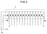
- the horizontal aging circuit 5 for example, as shown in FIG. 2, is provided with PMOS switches PSW, comprised of p-channel MOS (PMOS) transistors whose gates are connected to a control signal line LCTL, between all source lines Ls and one signal line LSG and is configured so that all source lines Ls can be driven by one interconnection.
- PMOS switches PSW comprised of p-channel MOS (PMOS) transistors whose gates are connected to a control signal line LCTL, between all source lines Ls and one signal line LSG and is configured so that all source lines Ls can be driven by one interconnection.
- the horizontal aging circuit 5 is provided on a seal region of the liquid crystal display panel 1, there is no disadvantage of the external size becoming larger due to formation of the horizontal aging circuit 5.
- the first pad region 6, as shown in FIG. 1, has mounted on it the horizontal drive circuit (HDRV) 8 in a TAB form at the time of actual use. Therefore, the first pad region 6 is provided with several hundreds of pads at pitches of about 80 ⁇ m corresponding to the source lines for the number of horizontal dots of the active matrix display area 2 and interconnections for vertical driving.
- HDRV horizontal drive circuit
- the second pad region 7 corresponds to the horizontal aging circuit 5 which drives all source lines Ls with one interconnection and is provided with not more than 10 pads including interconnections for vertical driving at pitches of about 500 ⁇ m.
- the pads and external horizontal drive circuit can be easily connected by bringing them into abutment by the naked eye.
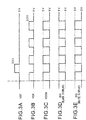
- FIGS. 3A to 3E are timing charts for when performing aging on this liquid crystal display panel 1.
- the timing charts indicate a case of VCOM inversion driving wherein a counter potential (VCOM) is inverted for every horizontal scanning period.
- VCOM counter potential
- FIG. 3C to FIG. 3E show VCOM and SIG switching between a solid line and dotted line for every field scanning period.
- FIG. 4 is a circuit diagram of an example of the configuration of a pixel cell of an active matrix display area.
- the pixel cell 10 is, as shown in FIG. 4, comprised of a TFT 11, a liquid crystal element (LC) 12, and a counter electrode (VCOM) 13. Such pixel cells are arranged in a matrix in the active matrix display area.
- a gate of the TFT 11 is connected to a gate line Lg, a source is connected to a source line Ls, and a drain is connected to a pixel electrode.
- the difference between the aging signal SIG supplied to the source line Ls and the counter potential VCOM becomes the potential applied to the liquid crystal, so as shown in FIG. 3C to FIG. 3E, by cyclically changing the VCOM and SIG for alternating driving, polarization of liquid crystal molecules can be prevented and the image quality can be improved.
- the horizontal aging circuit 5 and the vertical drive circuit 4 can be driven for white display and black display by using only the second pad region 7, i.e., even without using the first pad region 6, so aging for examining for defects of the panel itself can be performed.
- the present invention can be modified in various ways so long as no external drive circuit is mounted and an aging circuit is provided on a substrate of the liquid crystal display panel for enabling aging.
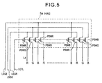
- the horizontal aging circuit 5 may be configured as shown in FIG. 5.
- source lines are gathered together for each of the three primary colors of R (red), G (green), and B (blue).
- the horizontal aging circuit 5a By using the horizontal aging circuit 5a, a monochrome raster can be displayed. Furthermore, by introducing a horizontal shift register circuit etc. to the horizontal aging circuit, a more complex image can be displayed at the time of aging.
- the source lines Ls are provided only with PMOS switches, but it is also possible to provide as switching means of the source lines Ls only NMOS switches comprised of n-channel MOS (NMOS) transistors or to provide CMOS switches.
- NMOS n-channel MOS
- the mode of connection of the external horizontal drive circuit and liquid crystal display panel is not limited to TAB. It may be COG etc. as well.
- FIG. 6 is a view of an example of the configuration of a circuit layout of a liquid crystal display panel when connecting an external drive circuit by COG.
- a horizontal aging circuit is provided on the substrate of the liquid crystal panel as explained above, while when a vertical drive circuit is connected as an external circuit to the liquid crystal display panel, a vertical aging circuit-is provided on the substrate of the liquid crystal display panel in the same way.
- both of a horizontal drive circuit and a vertical drive circuit are connected as external circuits, both of a horizontal aging circuit and a vertical aging circuit are provided on the substrate of the liquid crystal display panel.
- CMOS switches CMOS switches
- NMOS switches NMOS switches
- PMOS switches PMOS switches
- a method of producing a liquid crystal display panel of the present invention provided with a horizontal aging circuit or a vertical aging circuit or both on a substrate of the liquid crystal display panel it is sufficient to also form the horizontal aging circuit or vertical aging circuit in the process of forming the active matric display area on the substrate by the following well known method.
- the liquid crystal display panel of the present invention can be produced by a production method similar to that of a conventional liquid crystal panel for active matrix display, so there is no disadvantage of an increase of steps by providing the horizontal aging circuit or vertical aging circuit.
- an aging circuit is provided on the substrate of the liquid crystal display panel, therefore it is possible to perform aging and find potential panel defects by the substrate of the liquid crystal display panel alone. Therefore, a high quality liquid crystal display panel can be supplied at a low cost.
- a vertical drive circuit is integrally formed with the liquid crystal display area by using low temperature polycrystalline silicon (polySi) TFTs
- a horizontal drive circuit is connected to a liquid crystal display panel substrate by COG
- the output terminals of a driver IC composing the horizontal drive circuit and source lines are in a one-to-one correspondence.
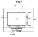
- FIG. 7 is a block diagram of a liquid crystal display apparatus 20 of an embodiment of the present invention.
- the liquid crystal display apparatus 20 comprises a liquid crystal display area (LDA) 22 formed on a glass substrate 21 by using low temperature polySi TFT, a vertical drive circuit 23 formed integrally with the liquid crystal display area 22 by using low temperature polySi TFTs, and an external horizontal drive circuit (HDRV) 24 mounted by COG.
- LDA liquid crystal display area
- HDRV external horizontal drive circuit
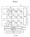
- FIG. 8 is a view of a specific circuit example of the liquid crystal display apparatus 20 of FIG. 7.
- the source lines of the liquid crystal display apparatus 20 are driven by a shift register circuit (SFT) 25, a sampling circuit (SMPL) 26, a latch circuit (LTC) 27, a digital/analog conversion circuit (DAC) 28, and an output buffer circuit (BUF) 29 configured in the driver IC of the COG connected horizontal drive circuit 24.
- SFT shift register circuit
- SPL sampling circuit
- LTC latch circuit
- DAC digital/analog conversion circuit
- BAF output buffer circuit
- the shift register 25 successively outputs horizontal scanning pulses to perform horizontal scanning.
- the sampling circuit 26 performs successive sampling on a digital image data input here in correspondence with the horizontal scanning pulses from the shift register circuit 25.
- the image data sampled in the sampling circuit 26 is stored for an amount of one horizontal period in the latch circuit 27.
- digital data of one horizontal period output from the latch circuit 27 is converted to an analog signal and output.
- the output from the output buffer circuit 29 is led to the source lines Ls of the liquid crystal display panel as it is.
- the output to the source lines Ls continues for one horizontal scanning period.
- the output terminals of the driver IC constituting the horizontal drive circuit 24 and the source lines are in a one-to-one correspondence.
- the vertical drive circuit 23 opens the TFT switch 11 for every gate line Lg in synchronization with switching of the source lines Ls. As a result, writing is performed in the order of the lines for every horizontal scan of the pixels.
- a first electrode is connected to a connection point of a drain of the TFT and a pixel electrode, and a second electrode has a held capacity 14 connected to the gate line Lg.
- liquid crystal display apparatus 20 as the driving method of the liquid crystal, alternating driving wherein the voltage applied to the liquid crystal is inverted each field is preferable.
- the number of connection points with an external circuit is the total of the amount of source lines of effective pixels on the horizontal drive circuit 24 side and about 10 pins for the vertical drive circuit 23.
- connection points becomes 320 pins in a liquid crystal display panel having 100 x 100 effective pixels. Accordingly, it is possible to gather together the connection pins at only one side of the four-sided liquid crystal display panel to mount an external circuit.
- the vertical drive circuit 23 and the liquid crystal display area 22 are formed integrally on the glass substrate 21 by using low temperature polySi TFTs.
- low temperature polySi TFTs can be produced by a 450°C or less low temperature film forming technique, so a normal glass substrate can be used instead of a quartz glass substrate.
- the liquid crystal display apparatus of the present invention can be produced at a low cost from this viewpoint as well.
- the TFTs formed by the low temperature polySi may be top gate types or bottom gate types.
- the horizontal drive circuit is connected to the liquid crystal display panel substrate by COG.
- COG liquid crystal display panel substrate
- the liquid crystal display apparatus of the present invention since the liquid crystal display apparatus of the present invention does not use a time sharing driving method and has the horizontal drive circuit as an external circuit, the image quality can be improved. Also, the yield of products is improved and production at a low cost can be attained. Particularly, the liquid crystal display apparatus of the present invention is advantageous as a medium- to small-sized liquid crystal display apparatus used for a PDA etc.
- an aging circuit is provided on a substrate of the liquid crystal display panel instead of an external horizontal drive circuit or a vertical drive circuit, so aging can be performed by the substrate of the liquid crystal display panel alone, potential panel defects can be found, and a high quality liquid crystal display panel can be supplied at a low cost.
- the liquid crystal display apparatus since a time sharing driving method is not used and a horizontal drive circuit is provided as an external circuit, the image quality can be improved, the yield of products is improved, and production at a low cost can be attained.
Landscapes
- Physics & Mathematics (AREA)
- Nonlinear Science (AREA)
- General Physics & Mathematics (AREA)
- Optics & Photonics (AREA)
- Crystallography & Structural Chemistry (AREA)
- Chemical & Material Sciences (AREA)
- Mathematical Physics (AREA)
- Engineering & Computer Science (AREA)
- Computer Hardware Design (AREA)
- Theoretical Computer Science (AREA)
- Liquid Crystal (AREA)
- Liquid Crystal Display Device Control (AREA)
- Devices For Indicating Variable Information By Combining Individual Elements (AREA)
- Control Of Indicators Other Than Cathode Ray Tubes (AREA)
Abstract
Description
Claims (10)
- A liquid crystal display panel comprising an active matrix display area, a vertical drive circuit, and a horizontal aging circuit for supplying signals to a plurality of source lines at one time provided on a substrate of the liquid crystal display panel and a horizontal drive circuit connected outside.
- A liquid crystal display panel comprising an active matrix display area, a horizontal drive circuit, and a vertical aging circuit for supplying signals to a plurality of gate lines at one time provided on a substrate of the liquid crystal display panel and a vertical drive circuit connected outside.
- A liquid crystal display panel comprising an active matrix display area, a horizontal aging circuit for supplying signals to a plurality of source lines at one time, and a vertical aging circuit for supplying signals to a plurality of gate lines at one time provided on a substrate of the liquid crystal display panel and a horizontal drive circuit and a vertical drive circuit connected outside.
- A liquid crystal display panel as set forth in claim 1, wherein a horizontal aging circuit or a vertical aging circuit gathers together a plurality of source lines or gate lines via CMOS switches, NMOS switches, or PMOS switches and supplies signals to the collected lines.
- A liquid crystal display panel as set forth in claim 2, wherein a horizontal aging circuit or a vertical aging circuit gathers together a plurality of source lines or gate lines via CMOS switches, NMOS switches, or PMOS switches and supplies signals to the collected lines.
- A liquid crystal display panel as set forth in claim 3, wherein a horizontal aging circuit or a vertical aging circuit gathers together a plurality of source lines or gate lines via CMOS switches, NMOS switches, or PMOS switches and supplies signals to the collected lines.
- A method of producing a liquid crystal display panel comprising an active matrix display area, a vertical drive circuit, and a horizontal aging circuit for supplying signals to a plurality of source lines at one time provided on a substrate of the liquid crystal display panel and a horizontal drive circuit connected outside, said method of producing a liquid crystal display planel comprising forming the horizontal aging circuit in a process of forming the active matrix display area on the substrate.
- A method of producing a liquid crystal display panel comprising an active matrix display area, a horizontal drive circuit, and a vertical aging circuit for supplying signals to a plurality of gate lines at one time provided on a substrate of the liquid crystal display panel and a vertical drive circuit connected outside, said method of producing a liquid crystal display planel comprising forming the vertical aging circuit in a process of forming the active matrix display area on the substrate.
- A method of producing a liquid crystal display panel comprising an active matrix display area, a horizontal aging circuit for supplying signals to a plurality of source lines at one time, and a vertical aging circuit for supplying signals to a plurality of gate lines at one time provided on a substrate of the liquid crystal display panel and a horizontal drive circuit and a vertical drive circuit connected outside, said method of producing a liquid crystal display planel comprising forming the horizontal aging circuit and the vertical aging circuit in a process of forming the active matrix display area on the substrate.
- A liquid crystal display apparatus of an active matrix type, wherein
a vertical drive circuit is formed integrally with a liquid crystal display area on a glass substrate by using low temperature polySi TFTs, a horizontal drive circuit is connected to a liquid crystal display panel substrate by COG, and output terminals of a driver IC constituting the horizontal drive circuit and source lines are in a one-to-one correspondence.
Applications Claiming Priority (5)
| Application Number | Priority Date | Filing Date | Title |
|---|---|---|---|
| JP2000230993 | 2000-07-31 | ||
| JP2000231013 | 2000-07-31 | ||
| JP2000230993A JP2002040464A (en) | 2000-07-31 | 2000-07-31 | LCD panel |
| JP2000231013A JP2002040483A (en) | 2000-07-31 | 2000-07-31 | Liquid crystal display |
| PCT/JP2001/006547 WO2002010851A1 (en) | 2000-07-31 | 2001-07-30 | Liquid crystal display panel and method for manufacturing the same, and liquid crystal display |
Publications (2)
| Publication Number | Publication Date |
|---|---|
| EP1220018A1 true EP1220018A1 (en) | 2002-07-03 |
| EP1220018A4 EP1220018A4 (en) | 2006-08-16 |
Family
ID=26597033
Family Applications (1)
| Application Number | Title | Priority Date | Filing Date |
|---|---|---|---|
| EP01954377A Ceased EP1220018A4 (en) | 2000-07-31 | 2001-07-30 | LIQUID CRYSTAL DISPLAY PANEL AND MANUFACTURING METHOD THEREOF, AND LIQUID CRYSTAL DISPLAY |
Country Status (7)
| Country | Link |
|---|---|
| US (1) | US6985128B1 (en) |
| EP (1) | EP1220018A4 (en) |
| KR (1) | KR100822332B1 (en) |
| CN (1) | CN1210608C (en) |
| NO (1) | NO326879B1 (en) |
| TW (1) | TWI240905B (en) |
| WO (1) | WO2002010851A1 (en) |
Cited By (5)
| Publication number | Priority date | Publication date | Assignee | Title |
|---|---|---|---|---|
| WO2007034364A1 (en) * | 2005-09-19 | 2007-03-29 | Koninklijke Philips Electronics N.V. | Display devices and row voltage generation circuits |
| EP1708166A3 (en) * | 2005-03-31 | 2009-04-08 | Himax Technologies, Inc. | Chip-on-glass liquid crystal display and data transmission method for the same |
| US7522159B2 (en) | 2002-11-08 | 2009-04-21 | Semiconductor Energy Laboratory Co., Ltd. | Display appliance |
| US8040312B2 (en) | 2005-03-11 | 2011-10-18 | Himax Technologies Limited | Chip-on-glass liquid crystal display and data transmission method for the same |
| CN103280173A (en) * | 2012-09-28 | 2013-09-04 | 武汉天马微电子有限公司 | Detection device and detection method of liquid crystal display panel |
Families Citing this family (14)
| Publication number | Priority date | Publication date | Assignee | Title |
|---|---|---|---|---|
| CN1312482C (en) * | 2003-07-09 | 2007-04-25 | 友达光电股份有限公司 | semiconductor accelerometer |
| CN100371718C (en) * | 2003-07-10 | 2008-02-27 | 友达光电股份有限公司 | capacitive acceleration sensor |
| CN100375916C (en) * | 2003-09-29 | 2008-03-19 | 友达光电股份有限公司 | LCD Module |
| US7427985B2 (en) * | 2003-10-31 | 2008-09-23 | Au Optronics Corp. | Integrated circuit for driving liquid crystal display device |
| CN1303578C (en) * | 2004-08-12 | 2007-03-07 | 友达光电股份有限公司 | Shunt access device and method for glass substrate |
| CN100594539C (en) * | 2005-03-31 | 2010-03-17 | 奇景光电股份有限公司 | source driver |
| KR101166585B1 (en) * | 2005-12-01 | 2012-07-18 | 엘지디스플레이 주식회사 | Flat panel display device having aging pad for preventing an electro static |
| TWI326439B (en) * | 2005-12-23 | 2010-06-21 | Chimei Innolux Corp | Liquid crystal display device and driving method therewith |
| KR101321256B1 (en) * | 2006-06-27 | 2013-10-25 | 엘지디스플레이 주식회사 | Liquid crystal display device |
| KR101363728B1 (en) * | 2006-12-26 | 2014-02-14 | 엘지디스플레이 주식회사 | Liquid crystal display device and method of aging the same |
| KR100853540B1 (en) | 2007-02-01 | 2008-08-21 | 삼성에스디아이 주식회사 | Organic light emitting display device and aging method |
| JP5649858B2 (en) * | 2009-10-23 | 2015-01-07 | 京セラディスプレイ株式会社 | Liquid crystal display device, liquid crystal display panel drive device, and liquid crystal display panel |
| KR102370385B1 (en) | 2015-02-05 | 2022-03-07 | 삼성디스플레이 주식회사 | Photomask layouts, methods of forming patterns using the same and methods of manufacturing display devices using the same |
| CN109407434B (en) | 2018-11-22 | 2020-11-24 | 武汉华星光电技术有限公司 | Liquid crystal display device having a plurality of pixel electrodes |
Family Cites Families (14)
| Publication number | Priority date | Publication date | Assignee | Title |
|---|---|---|---|---|
| JPH01130132A (en) | 1987-11-16 | 1989-05-23 | Seiko Epson Corp | Active matrix substrate |
| JP2755689B2 (en) * | 1989-06-12 | 1998-05-20 | 株式会社東芝 | Liquid crystal display integrated circuit and liquid crystal display device |
| US5849601A (en) * | 1990-12-25 | 1998-12-15 | Semiconductor Energy Laboratory Co., Ltd. | Electro-optical device and method for manufacturing the same |
| JPH04288588A (en) | 1991-03-18 | 1992-10-13 | Matsushita Electron Corp | Active matrix type liquid crystal display device |
| US5841414A (en) * | 1994-08-16 | 1998-11-24 | Citizen Watch Co., Ltd. | Liquid crystal display device |
| JPH08201841A (en) * | 1994-11-24 | 1996-08-09 | Toshiba Electron Eng Corp | Display device and its inspection method |
| KR100195501B1 (en) * | 1995-11-30 | 1999-06-15 | 김영남 | Flat panel display data driving device using latch type transmitter |
| KR0163938B1 (en) * | 1996-01-13 | 1999-03-20 | 김광호 | Driving circuit of thin film transistor liquid crystal device |
| JPH1010546A (en) | 1996-06-19 | 1998-01-16 | Furon Tec:Kk | Display device and its driving method |
| US6292182B1 (en) * | 1997-06-25 | 2001-09-18 | Hyundai Electronics Industries Co., Ltd. | Liquid crystal display module driving circuit |
| JP3667548B2 (en) * | 1998-03-27 | 2005-07-06 | シャープ株式会社 | Active matrix type liquid crystal display panel and inspection method thereof |
| JP4357613B2 (en) | 1998-10-27 | 2009-11-04 | シャープ株式会社 | LCD with integrated driver |
| US6771239B1 (en) * | 1999-05-17 | 2004-08-03 | Seiko Epson Corporation | Method for manufacturing an active matrix substrate |
| KR100759967B1 (en) * | 2000-12-16 | 2007-09-18 | 삼성전자주식회사 | Flat panel display |
-
2000
- 2000-07-30 US US10/089,230 patent/US6985128B1/en not_active Expired - Lifetime
-
2001
- 2001-07-30 WO PCT/JP2001/006547 patent/WO2002010851A1/en not_active Ceased
- 2001-07-30 EP EP01954377A patent/EP1220018A4/en not_active Ceased
- 2001-07-30 CN CNB018022375A patent/CN1210608C/en not_active Expired - Fee Related
- 2001-07-30 KR KR1020027003742A patent/KR100822332B1/en not_active Expired - Fee Related
- 2001-07-31 TW TW090118652A patent/TWI240905B/en not_active IP Right Cessation
-
2002
- 2002-03-20 NO NO20021396A patent/NO326879B1/en not_active IP Right Cessation
Cited By (7)
| Publication number | Priority date | Publication date | Assignee | Title |
|---|---|---|---|---|
| US7522159B2 (en) | 2002-11-08 | 2009-04-21 | Semiconductor Energy Laboratory Co., Ltd. | Display appliance |
| US8040312B2 (en) | 2005-03-11 | 2011-10-18 | Himax Technologies Limited | Chip-on-glass liquid crystal display and data transmission method for the same |
| EP1708166A3 (en) * | 2005-03-31 | 2009-04-08 | Himax Technologies, Inc. | Chip-on-glass liquid crystal display and data transmission method for the same |
| WO2007034364A1 (en) * | 2005-09-19 | 2007-03-29 | Koninklijke Philips Electronics N.V. | Display devices and row voltage generation circuits |
| CN101268503B (en) * | 2005-09-19 | 2010-11-10 | 奇美电子股份有限公司 | display device and line voltage generating circuit |
| CN103280173A (en) * | 2012-09-28 | 2013-09-04 | 武汉天马微电子有限公司 | Detection device and detection method of liquid crystal display panel |
| CN103280173B (en) * | 2012-09-28 | 2016-08-10 | 武汉天马微电子有限公司 | Detection device and detection method of liquid crystal display panel |
Also Published As
| Publication number | Publication date |
|---|---|
| KR100822332B1 (en) | 2008-04-16 |
| NO20021396L (en) | 2002-05-14 |
| KR20020080326A (en) | 2002-10-23 |
| EP1220018A4 (en) | 2006-08-16 |
| CN1210608C (en) | 2005-07-13 |
| TWI240905B (en) | 2005-10-01 |
| WO2002010851A1 (en) | 2002-02-07 |
| CN1386211A (en) | 2002-12-18 |
| US6985128B1 (en) | 2006-01-10 |
| NO326879B1 (en) | 2009-03-09 |
| NO20021396D0 (en) | 2002-03-20 |
Similar Documents
| Publication | Publication Date | Title |
|---|---|---|
| US6985128B1 (en) | Liquid crystal display panel and production method of the same, and liquid crystal display apparatus | |
| KR100389605B1 (en) | Active matrix display device and inspection method for the same | |
| KR100242443B1 (en) | Liquid crystal panel for dot inversion driving and liquid crystal display device using the same | |
| KR100437947B1 (en) | A liquid crystal display device | |
| US5995073A (en) | Method of driving a liquid crystal display device with voltage polarity reversal | |
| US9190003B2 (en) | Display apparatus and method of manufacturing the same | |
| US8405593B2 (en) | Liquid crystal device with multi-dot inversion | |
| KR100954011B1 (en) | Display device | |
| CN101221337A (en) | Array substrate of liquid crystal display device and driving method | |
| CN101404146B (en) | Electrooptic device and electronic apparatus | |
| CN101216649A (en) | Array substrate of liquid crystal display device and driving method | |
| CN101216650A (en) | Array substrate of liquid crystal display device and driving method | |
| KR20090077669A (en) | Electro-optical devices, methods of driving electro-optical devices, electronic devices | |
| JP2001042287A (en) | Liquid crystal display device and driving method thereof | |
| KR20040047734A (en) | Display apparatus | |
| JP2009064041A (en) | On-glass single-chip LCD | |
| US20060146128A1 (en) | Method of driving display device and display device for performing the same | |
| KR100539841B1 (en) | Circuit for providing image signal and electrooptic panel | |
| US7750876B2 (en) | Electro-optical device and electronic apparatus with image signal conversion | |
| KR20080057501A (en) | LCD and its driving method | |
| JP3909526B2 (en) | Inspection method for active matrix display device | |
| JP4363881B2 (en) | Liquid crystal display | |
| KR20070120320A (en) | Manufacturing method of liquid crystal display and large area substrate for same | |
| US12451095B2 (en) | Display device | |
| JPH07287555A (en) | Liquid crystal display |
Legal Events
| Date | Code | Title | Description |
|---|---|---|---|
| PUAI | Public reference made under article 153(3) epc to a published international application that has entered the european phase |
Free format text: ORIGINAL CODE: 0009012 |
|
| AK | Designated contracting states |
Kind code of ref document: A1 Designated state(s): AT BE CH CY DE DK ES FI FR GB GR IE IT LI LU MC NL PT SE TR |
|
| 17P | Request for examination filed |
Effective date: 20020730 |
|
| RBV | Designated contracting states (corrected) |
Designated state(s): DE FR GB IT |
|
| RIC1 | Information provided on ipc code assigned before grant |
Ipc: G02F 1/13 20060101AFI20060401BHEP Ipc: G09G 3/00 20060101ALI20060401BHEP Ipc: G02F 1/1362 20060101ALI20060401BHEP Ipc: G09G 3/36 20060101ALI20060401BHEP |
|
| A4 | Supplementary search report drawn up and despatched |
Effective date: 20060714 |
|
| 17Q | First examination report despatched |
Effective date: 20061120 |
|
| RAP1 | Party data changed (applicant data changed or rights of an application transferred) |
Owner name: JAPAN DISPLAY WEST INC. |
|
| REG | Reference to a national code |
Ref country code: DE Ref legal event code: R003 |
|
| STAA | Information on the status of an ep patent application or granted ep patent |
Free format text: STATUS: THE APPLICATION HAS BEEN REFUSED |
|
| 18R | Application refused |
Effective date: 20160229 |