EP1219984A2 - Photonic crystal waveguide - Google Patents
Photonic crystal waveguide Download PDFInfo
- Publication number
- EP1219984A2 EP1219984A2 EP01310803A EP01310803A EP1219984A2 EP 1219984 A2 EP1219984 A2 EP 1219984A2 EP 01310803 A EP01310803 A EP 01310803A EP 01310803 A EP01310803 A EP 01310803A EP 1219984 A2 EP1219984 A2 EP 1219984A2
- Authority
- EP
- European Patent Office
- Prior art keywords
- photonic crystal
- dimensional photonic
- waveguide
- dielectric
- crystal slab
- Prior art date
- Legal status (The legal status is an assumption and is not a legal conclusion. Google has not performed a legal analysis and makes no representation as to the accuracy of the status listed.)
- Granted
Links
Images




Classifications
-
- G—PHYSICS
- G02—OPTICS
- G02B—OPTICAL ELEMENTS, SYSTEMS OR APPARATUS
- G02B6/00—Light guides; Structural details of arrangements comprising light guides and other optical elements, e.g. couplings
- G02B6/10—Light guides; Structural details of arrangements comprising light guides and other optical elements, e.g. couplings of the optical waveguide type
- G02B6/12—Light guides; Structural details of arrangements comprising light guides and other optical elements, e.g. couplings of the optical waveguide type of the integrated circuit kind
- G02B6/13—Integrated optical circuits characterised by the manufacturing method
-
- B—PERFORMING OPERATIONS; TRANSPORTING
- B82—NANOTECHNOLOGY
- B82Y—SPECIFIC USES OR APPLICATIONS OF NANOSTRUCTURES; MEASUREMENT OR ANALYSIS OF NANOSTRUCTURES; MANUFACTURE OR TREATMENT OF NANOSTRUCTURES
- B82Y20/00—Nanooptics, e.g. quantum optics or photonic crystals
-
- G—PHYSICS
- G02—OPTICS
- G02B—OPTICAL ELEMENTS, SYSTEMS OR APPARATUS
- G02B6/00—Light guides; Structural details of arrangements comprising light guides and other optical elements, e.g. couplings
- G02B6/10—Light guides; Structural details of arrangements comprising light guides and other optical elements, e.g. couplings of the optical waveguide type
- G02B6/12—Light guides; Structural details of arrangements comprising light guides and other optical elements, e.g. couplings of the optical waveguide type of the integrated circuit kind
- G02B6/122—Basic optical elements, e.g. light-guiding paths
- G02B6/1225—Basic optical elements, e.g. light-guiding paths comprising photonic band-gap structures or photonic lattices
Definitions
- the present invention relates to a photonic crystal waveguide which can be used as a basic structure which forms photonic devices such as lasers and photonic ICs used for optical information processing, optical transmission and the like.
- the photonic crystal is expected to be a new photonic material which can solve the above-mentioned problem, in which the photonic crystal can perform light confinement by a concept completely different from the conventional one.
- the photonic crystal has an artificial multidimensional periodic structure in which periodicity, which is almost the same as light wavelength, is formed by using more than one kinds of mediums having different refractive indices, and the photonic crystal has a band structure of light similar to a band structure of electron. Therefore, forbidden band of light (photonic band-gap) appears in a specific structure so that the photonic crystal having the specific structure functions as a nonconductor for light.
- Joannopoulos and others applied a line defect in a two-dimensional photonic crystal in which cylindrical columns having large refractive index almost the same as that of a semiconductor are arranged on a square lattice of lattice constant "a" which is about light wavelength and the radius of each cylindrical column is a/5, and, J. D. Joannopoulos and others theoretically indicated that an optical waveguide having no scattering loss even when it is steeply bent can be realized. This waveguide can be very important for realizing a large scale integrated optical circuit.
- the optical waveguide for forming the large scale integrated optical circuit it is necessary to realize a single waveguiding mode in the photonic band-gap frequency band.
- a multi-mode waveguide having a plurality of modes is used as a bent waveguide, there is a problem, for example, in that a part of mode may be converted into a different mode in a bending part.
- the multi-mode waveguide can not be used as an effective bent waveguide necessary for realizing the large scale integrated optical circuit. That is the reason for requiring the single-mode.
- the multi-mode waveguide is not suitable for high-speed communication.
- waveguides Some types have been manufactured. In the various waveguides, waveguides using the two-dimensional photonic crystal is promising since it is very difficult to fabricate waveguides by a three-dimensional photonic crystal which has full band-gap.
- the two-dimensional photonic crystal slab on oxide cladding is based on a structure in which a thin semiconductor film of high refractive index (from 3 to 3.5) is deposited on a dielectric of low refractive index (oxide or polymer in many cases, the refractive index is about 1.5).
- SOI substrate is being applied to LSIs, and high-quality SOI substrate can be manufactured in recent years.
- the SOI substrate is formed by providing a silicon (Si) thin-film on silica (SiO 2 ).
- Si silicon
- SiO 2 silicon
- the two-dimensional photonic crystal slab on oxide cladding having high quality can be easily manufactured.
- the merit can not be obtained by using other structures (for example, two-dimensional photonic crystal air-bridge slab in which cladding of both sides is air).
- the two-dimensional photonic crystal slab on oxide cladding has the advantage of being easier to manufacture than the two-dimensional photonic crystal air-bridge slab and the like.
- the structure has following problems so that the single waveguiding mode was not realized in the photonic band-gap frequency band according to the conventional structure.
- Figs.1A and 1B are schematic diagrams of a structure of a single missing-hole line defect photonic crystal waveguide of a typical air-hole type according to a conventional technology.
- Fig.1A shows a top view
- Fig.1B shows a B-B' section view.
- the conventional single missing-hole line defect photonic crystal waveguide can be also called as a normal two-dimensional photonic crystal slab waveguide in this specification.
- 5 indicates an optical waveguide part
- 2 indicates an Si layer
- 3 indicates an SiO 2 layer which is a cladding layer
- 4 indicates an air-hole triangle lattice point, in which the lattice constant is represented as "a".
- Each air-hole is a cylindrical column or a polygon column which penetrates the Si layer 2.
- the diameter of the air-hole is 0.215 ⁇ m in this example.
- the air-hole is placed in each lattice point of the triangle lattice.
- the triangle lattice is a regular lattice in which lattice points are placed on vertices of regular triangles which are arranged over the two-dimensional plane.
- two-dimensional photonic crystals having the photonic band-gap there are two structures.
- One is a structure in which columns of high refractive index are provided in air.
- Another is a structure in which air-holes are provided in a high refractive index layer like the above-mentioned example.
- the air-hole can be also called a low refractive index column or a low refractive index cylindrical column.
- the former structure which was used by J. D. Joannopoulos and others, requires a cladding layer for supporting the columns.
- the refractive index of the cladding layer is larger than that of the air which is a core for the line defect waveguide, very long columns are necessary for preventing light leakage to the upper and lower sides so that manufacturing such structure becomes very difficult.
- the cladding layer can be freely chosen, and it is easy to determine a core having refractive index larger than that of the cladding layer.
- limitation on manufacturing is small so that it is easy to select structural condition that light hardly leak to the upper and lower sides.
- the holes can be placed on the two-dimensional plane of the high refractive index plate of the photonic crystal in various way, a structure in which the holes (cylindrical columns or polygon columns) are arranged in a triangle lattice pattern is known to have the photonic band-gap ranging over a wide frequency band. This means that this structure functions as a nonconductor for light in wide frequency band. This structure is preferable since frequency can be selected from wide rage frequencies when designing a waveguide.
- Fig.2 shows a dispersion relation of waveguiding modes of a conventional typical single missing-hole line defect photonic crystal waveguide.
- the waveguiding modes become as shown in Fig.2.
- normalized frequency represented by (lattice constant/wavelength) which is a dimensionless number is used.
- normalized propagation constant represented by (wave number ⁇ lattice constant/2 ⁇ ) is used.
- the light line of the cladding SiO 2 , refractive index 1.46) is also shown in Fig.2.
- the waveguiding mode which satisfies the condition that light does not leak to the cladding layer is only in a region circled by an ellipse which is below the light line.
- group velocity (energy propagation velocity) of the waveguiding mode which is determined depending on the inclination, is very small.
- group velocity energy propagation velocity
- the mode of very small group velocity is affected by the heterogeneity so that light may not propagate.
- the inventors actually manufactured the conventional single missing-hole line defect photonic crystal waveguide. However, light propagation was not detected at all. The cause of the problem is that there is no realistically usable waveguiding mode which has a group velocity which is not too small below the light line, and that the diffraction loss is very large in the region above the light line.
- the waveguiding mode As long as the oxide cladding structure is used, since the position of the light line is determined by the refractive index of the cladding, the position of the light line can not be changed largely.
- the waveguiding mode As long as the single-mode within the band-gap should be used, it is difficult to obtain a waveguiding mode having large group velocity below the light line by using the structure shown in Fig.1. As for crystal structures other than the triangle lattice such as square lattice, it is more difficult to obtain such waveguiding mode. Therefore, it is very difficult to use waveguiding modes below the light line.
- Figs. 3A-3C are figures for explaining the conventional single missing-hole line defect photonic crystal waveguide (optical waveguide).
- Fig.3A shows a top view of the optical waveguide
- Fig.3B shows an A-A' section view
- Fig.3C shows a B-B' section view.
- the optical waveguide 30 includes dielectric thin-film slab 31 (which corresponds to the above-mentioned high refractive index plate) sandwiched between a top cladding layer 36 and a bottom cladding layer 37.
- a photonic crystal structure is formed in the dielectric thin-film slab 31 by providing low refractive index cylindrical columns 35 having lower refractive index than that of the dielectric thin-film slab 31 in a triangle lattice pattern.
- one line of the low refractive index cylindrical columns 35 is replaced by a dielectric having the same refractive index as the dielectric thin-film slab 31 such that the part of the one line can be used as an optical waveguide part 32.
- Arrows ⁇ in the optical waveguide part 32 indicate optical propagation directions.
- the waveguide shown in Fig.1 is an example of a structure shown in Fig.3 in which the top cladding layer 36 and the low refractive index cylindrical column 35 are air, the bottom cladding layer 37 is SiO 2 , and the dielectric thin-film slab 31 is Si.
- the low refractive index cylindrical column 35 having the refractive index 1.0 is the same as an air-hole. Characteristics of the optical waveguide 30 will be described in the following.
- These refractive indices of the optical waveguide 30 correspond to those of Si, air (vacuum) and SiO 2 which are often used for forming waveguides targeted for infrared light for optical communication having a wavelength about 1.55 ⁇ m.
- relative dielectric constant corresponds to a square of refractive index
- dielectric constant can be used instead of "refractive index” in this specification.
- Figs.4A-4C are figures for explaining waveguiding modes of the above-mentioned optical waveguide.
- Fig.4A shows dispersion curves of waveguiding modes which can propagate through the optical waveguide part.
- the dispersion curves of waveguiding modes are obtained by using a plane wave expansion method (R.D.Meade et al.,Physical Review B 48,8434(1993)) to which periodic boundary condition is applied.
- This figure is similar to Fig.2.
- Fig.4B shows magnetic field component perpendicular to the dielectric thin-film slab according to a mode 1 in Fig.4A
- Fig.4C shows magnetic field component perpendicular to the dielectric thin-film slab according to a mode 2 in Fig.4A.
- Fig.4A Each amount in Fig.4A is normalized by the lattice constant or speed of light c.
- the diagonally shaded regions correspond to the outside of photonic band-gap (J D. JoannoPoulos, R D. Meade,J N.Winn, "Photonic Crystals", Princeton University Press, Princeton (1995)), that is, the diagonally shaded areas show regions in which light can not be confined in the optical waveguide part 32 (A.Mekis et al.,Physical Review B 58,4809(1998)).
- the vertical line hatching region In the vertical line hatching region, power of light confinement caused by difference of refractive indices between the dielectric thin-film slab 31 and the top cladding layer 36/bottom cladding layer 37 is weakened so that light can not be confined in the optical waveguide part 32 (S G. Johnson et al., Physical Review B 60,5751 (1999)).
- the vertical line hatching region corresponds to the before-mentioned above region of the light line. That is, a region to be considered used for the waveguide is only a white region in Fig.4A.
- two waveguiding modes 1 and 2 exist in the white region of the conventional optical waveguide 30. Further waveguiding modes may exist when the band-gap is wider, however, the two modes 1 and 2 will be considered here for the sake of simplicity.
- the mode 1 corresponds to the mode circled by the ellipse in Fig.2, and the mode 2 corresponds to the mode of upper dotted line.
- the mode 1 in the low frequency side generally has magnetic field distribution shown in Fig.4B
- the mode 2 in the high frequency side generally has magnetic field distribution shown in Fig.4C.
- the mode 1 is practical since the mode 1 has electric field distribution almost the same as that of a general single-mode waveguide.
- electric field distribution of the mode 2 is largely different from that of the general signal-mode waveguide. Therefore, it is difficult to conduct light from an outside circuit by using the mode 2. That is, the mode 2 is not a practical waveguiding mode.
- waveguiding modes of higher frequency side which appears when the band-gap is wide is not practical since the waveguiding mode is largely different from that of the general single-mode waveguide.
- the mode 1 is used for the conventional waveguide.
- the mode 1 since the frequency hardly change even when the propagation constant change in this mode 1, the mode 1 has a defect that usable frequency band is very small.
- the frequency band is about 1%.
- the conventional waveguide has a defect that transmission time becomes very long, and propagation loss due to absorption and scattering loss in waveguide becomes large.
- An object of the present invention is to solve the above-mentioned problems in the photonic crystal waveguide and to provide a two-dimensional photonic crystal slab waveguide allowing single-mode transmission in which group velocity is increased and propagation loss is decreased.
- the above object can be achieved by a two-dimensional photonic crystal slab waveguide in which a part of holes in a lattice structure of a two-dimensional photonic crystal slab do not exist linearly so that a line defect is formed, wherein:
- the first width may a value from 0.5 times to 0.85 times of the second width.
- the first width which is a distance between centers of nearest two lattice points located on both sides of the line defect is different from the second width which is a corresponding distance in a normal two-dimensional photonic crystal slab waveguide
- an optical waveguide which can form a single waveguiding mode having large group velocity below the light line can be provided.
- the two-dimensional photonic crystal slab waveguide may be called a single missing-hole line defect photonic crystal waveguide.
- the lattice structure may be formed by air-hole triangle lattices, and the two-dimensional photonic crystal slab waveguide may include an oxide cladding or a polymer cladding.
- the two-dimensional photonic crystal slab waveguide may be formed by using a Silicon-On-Insulator (SOI) substrate.
- SOI Silicon-On-Insulator
- the first width may be wider than the second width in which a single-mode appears in a high frequency side of a light line of cladding in a dispersion relation of waveguiding modes of the two-dimensional photonic crystal slab waveguide having the first width, and the first width may a value from 1.3 times to 1.6 times of the second width.
- an optical waveguide can be provided which can form a single waveguiding mode of low loss above the light line can be provided.
- the above object can be also achieved by a two-dimensional photonic crystal slab waveguide in which dielectric cylindrical or polygon columns having lower refractive index than that of a dielectric thin-film slab are provided in then dielectric thin-film slab in a two-dimensional lattice pattern, and the dielectric thin-film slab is sandwiched by a top cladding layer and a bottom cladding layer which have lower refractive index than that of the dielectric thin-film slab, wherein:
- the dielectric columns in an optical waveguide part in the two-dimensional photonic crystal slab waveguide are located at positions which are shifted in an optical propagation direction from positions at which the dielectric columns should be positioned in a normal two-dimensional photonic crystal slab.
- an optical waveguide which can form a single waveguiding mode having large group velocity below the light line can be provided.
- the dielectric cylindrical or polygon columns, or the dielectric columns are low refractive index columns having lower refractive index than that of the dielectric thin-film slab.
- a first diameter of the dielectric columns in the optical waveguide part may be different from a second diameter of other dielectric columns located in parts other than the optical waveguide part, and the first diameter is a value by which the dielectric columns does not contact with the other dielectric columns.
- positions of dielectric columns which form one line of the lattice of two-dimensional photonic crystal slab for an optical waveguide part may be shifted in an optical propagation direction by a half of the lattice constant of the normal two-dimensional photonic crystal slab.
- each dielectric column of dielectric columns in the optical waveguide part may be apart from a position at which the each dielectric column should be positioned in the normal two-dimensional photonic crystal slab by a half of the lattice constant of the normal two-dimensional photonic crystal slab.
- the dielectric cylindrical or polygon columns may be arranged in a triangle lattice pattern having a lattice constant "a", a radius or a half-breadth of the dielectric cylindrical or polygon columns is from 0.2a to 0.45a, and the radius or half-breadth is determined such that the dielectric cylindrical or polygon columns do not contact with dielectric columns in the optical waveguide part.
- a refractive index of the dielectric thin-film slab may be from 3.0 to 4.5, and each of refractive indices of parts other than the dielectric thin-film slab may be from 1.0 to 1.7.
- the dielectric cylindrical or polygon columns may be arranged in a square lattice pattern having a lattice constant "a", a radius or a half-breadth of the dielectric cylindrical or polygon columns is from 0.35a to 0.45a, and the radius or half-breadth is determined such that wherein the dielectric cylindrical or polygon columns do not contact with dielectric columns in the optical waveguide part.
- silicon, germanium, gallium arsenide base compound, indium phosphide base compound, or indium antimony base compound may be used as a material of the dielectric thin-film slab
- silica, polyimide base organic compound, epoxy base organic compound, acrylic base organic compound, air or vacuum may be used as a material of parts other than the dielectric thin-film slab.
- the optical waveguide in the embodiments is structured such that, in a two-dimensional photonic crystal slab waveguide in which a part of holes in a lattice structure of a two-dimensional photonic crystal slab do not exist linearly so that a line defect is formed, a first width which is a distance between centers of nearest two lattice points located on both sides of the line defect is narrower (first embodiment) or wider (second embodiment) from a second width which is a distance between centers of nearest two lattice points located on both sides of a line defect in a normal two-dimensional photonic crystal slab waveguide which simply lacks holes of a single line.
- the same effect can be obtained by shifting the position of one line of low refractive index columns (air-holes and the like) in the light propagation direction, or, in addition to that, by changing the radius of the holes (third embodiment).
- the two-dimensional photonic crystal slab is a photonic crystal in which dielectric cylindrical or polygon columns having lower refractive index than that of a dielectric thin-film slab are provided in the dielectric thin-film slab in a two-dimensional lattice pattern, and the dielectric thin-film slab is sandwiched by a top cladding layer and a bottom cladding layer which have lower refractive index than that of said dielectric thin-film slab.
- the top or bottom cladding layer and/or the dielectric cylindrical or polygon columns may be air or vacuum.
- Figs.5A and 5B are figures showing a structure of a single missing-hole line defect photonic crystal waveguide according to a first embodiment of the present invention.
- the single missing-hole line defect photonic crystal waveguide can also be called as a two-dimensional photonic crystal slab waveguide.
- Fig.5A shows a top view
- Fig.5B shows a B-B' section view.
- single line defect is formed in a two-dimensional photonic crystal slab on oxide cladding by removing holes of the single line, and, width of the line defect (in other words, width of the optical waveguide part 5) is tuned by shifting positions of the whole crystal lattices of both sides of the line defect.
- the width of the line defect and the width of the optical waveguide part have the same meaning, in which the width is a distance between centers of nearest two lattice points located on both sides of the line defect.
- Tuning of the width of a waveguide part is performed by shifting crystal lattices of both sides of the line defect by a predetermined distance in a direction perpendicular to the line defect.
- the width of the line defect of a normal single missing-hole line defect photonic crystal waveguide (which may be called a normal width W) is defined as a distance between centers of nearest lattice points 4 of both sides of the line defect. Width of the line defect of this embodiment can be represented by a constant number - times of the normal width W.
- the photonic crystal itself has the photonic band-gap between a wavelength 1.35 ⁇ m and a wavelength 1.57 ⁇ m. Thus, transmission of light was not observed in a part having no defect in the crystal within the wavelength range. Next, light transmission spectrum for each line defect was measured. As for a simple (normal) single line defect (the width is 1.0W), light transmission was not observed in the photonic bad-gap frequency range. On the other hand, when using a waveguide having the width of 0.7W, light transmission was clearly observed in a frequency range of the photonic band-gap.
- Fig.6 shows a dispersion relation of waveguiding modes of the single missing-hole line defect photonic crystal waveguide according to the first embodiment of the present invention.
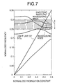
- Fig.2 can be represented as Fig.7 for comparing with Fig.6.
- the light line of the cladding (SiO 2 in this embodiment) is overlaid on Fig.7 like in Fig.6.
- a waveguiding mode (which corresponds to the mode 1 in Fig.4) below the light line of the normal waveguide (the width is 1.0W) has small inclination.
- a waveguiding mode which has large inclination that is, which has large group velocity exists below the light line in the photonic band-gap.
- the single-mode condition is satisfied in the region.
- a wavelength region in which light transmission was detected in an experiment is the same as the region where this waveguiding mode exists. This shows that the light transmission is realized since the single waveguiding mode having large group velocity is formed by decreasing the width of the line defect (optical waveguide part).
- the width of the line defect optical waveguide part
- light propagation was observed within the width range in experiments.
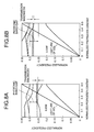
- Figs.8A and 8B show results of theoretical calculation of waveguiding mode dispersion in the cases where the width of the optical waveguide part is 0.85W and 0.50W.
- Fig.8A shows the case of 0.85W
- Fig.8b shows the case of 0.50W.
- the width of the optical waveguide part is a value between 0.85W and 0.50W
- the transmission bandwidth of the waveguiding mode is wider than those of the cases shown in Figs.8A and 8B as shown in Fig.6 (0.7W), for example. Therefore, it can be understood that the waveguide having the line defect within the width range practically functions.
- the mode in the typical (normal) single-line defect state as shown in Fig.2, the mode (circled mode in Fig.2) in the low frequency region below the light line within the photonic band-gap has very small group velocity. Thus, this mode is not practical.
- a waveguiding mode in the outside of the band-gap having large group velocity is considered.
- the mode of the lowest mode in Fig.2 can be shifted to the high frequency side by narrowing the width. Accordingly, this mode can be used within the photonic band-gap and below the light line. Therefore, it becomes possible that a mode having large group velocity can be realized within the band gap and below the light line.
- the refractive index of the waveguide can also be lowered by using a medium of low refractive index in the waveguide part, by providing holes in the line defect and the like. A method corresponding to providing holes in the line defect will be described in the third embodiment.
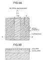
- Figs.9A and 9B are figures showing a structure of a single missing-hole line defect photonic crystal waveguide 1A according to a second embodiment of the present invention.
- Fig.9A shows a top view
- Fig.9B shows a B-B' section view.
- width of the line defect is widened by shifting the whole crystal lattice of both sides of the line defect.
- single waveguiding mode having a large group velocity can be obtained above the light line of the cladding.
- Tuning of the width of the optical waveguide part is performed by shifting crystal lattices of both sides of the line defect by a predetermined distance in a direction perpendicular to the line defect such that the width is widened.
- the width of the optical waveguide part is 1.5 times of the normal width of a normal optical waveguide part.
- the normal width of the line defect of a normal single missing-hole line defect photonic crystal waveguide is defined as a distance between centers of nearest lattice points 4 of both sides of the line defect of a normal single missing-hole line defect photonic crystal waveguide.
- Width of line defect of this embodiment can be represented by a constant number - times of the normal width W.
- the photonic crystal itself has the photonic band-gap between a wavelength 1.35 ⁇ m and a wavelength 1.57 ⁇ m. Thus, transmission of light was not observed in parts having no defect in the crystal within the wavelength range.
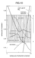
- Fig.10 shows a dispersion relation of waveguiding modes of the single missing-hole line defect photonic crystal waveguide according to the second embodiment of the present invention.
- the light line of the cladding SiO 2 in this embodiment
- the wavelength region in which light transmission was observed by an experiment is the same as a region within which an even mode exists in the single-mode region in Fig.10.
- the single-mode region exists in the photonic band-gap above the light line.
- the problem of light leaking is solved by widening the width of the optical waveguide part since diffraction loss decreases. That is, a waveguiding mode of low loss can be obtained although the waveguiding mode exists above the light line.
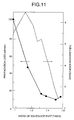
- Fig.11 shows dependence of bandwidth of single-mode above the light line (shown by dotted line) and propagation loss (shown by solid line) on the width of the optical waveguide part according to the second embodiment of the present invention.
- the bandwidth is normalized by a central frequency of the single-mode band.
- the bandwidth of the single-mode decreases after increasing, and, then, the single-mode bandwidth can not be obtained when the width exceeds 1.6W.
- the reason that the single-mode bandwidth changes in this way is that the mode in the photonic band-gap in Fig.10 shifts to the low frequency side by widening the waveguide width.
- the propagation loss decreases as the width is widened.
- the dispersion curve can be obtained by analyzing the Maxwell equation by using a calculation method called FDTD method (Finite-difference Time-domain method). In the following, the analyzing method will be described.
- FDTD method Finite-difference Time-domain method
- a periodic structure like crystal can be represented by repetition of a unit cell. It is well known that the field in such structure becomes Bloch wave.
- periodic boundary condition satisfying Bloch condition is applied to boundary of unit cells and fields which satisfies the condition are extracted as eigenmodes.
- the subject to be analyzed is Schrödinger equation. Since distribution of spatial potential is different according to material, various band structures may exist. This idea is applied to the photonic crystal which is a periodic dielectric structure.
- the equation to be considered is the Maxwell equation and refractive index (dielectric constant) distribution is used for calculation instead of potential distribution.
- the Maxwell equation is discretized in time and space into finite-difference equations, and electromagnetic field of light propagating in the structure (space distribution of the refractive index) is obtained by sequential calculation. That is, the FDTD method is not a method for directly obtaining the eigenvalue. However, the method can obtain modes of a given structure in the following way.
- a proper initial field is given in the structure. After performing the sequential calculation, fields applicable for the structure survive and other fields are not selected. By performing Fourier conversion on time variation of the field, frequency spectrum can be obtained. When there is a field applicable for the structure, a peak appears in the frequency spectrum. Since the Bloch condition used in the calculation is a function of wave number, the frequency at which the peak appears becomes a function of wave number. The band figure of the photonic crystal can be obtained by showing the function.
- mode calculation of the two-dimensional photonic crystal waveguide will be described. Basically, the same calculation as the above-mentioned one is performed.
- the line defect is incorporated in the inside of the crystal so that the periodicity is disturbed in the direction perpendicular to the line defect. Therefore, a structure shown in Figs.12A-12C is used as the unit cell. That is, the periodic boundary condition which satisfies the Bloch condition is applied in the propagation direction of the light.
- periodic structure is realized by using mirror boundary in which waveguides are placed such that large interference does not occur, and a region for absorbing leaking light which does not become a mode is provided in the thickness direction.
- Fig.12A shows the structure of Fig.1.
- Fig.12B is a magnified view of a part in a dotted line box of Fig.12A
- Fig.12C shows stereoscopic view of the structure of Fig.12B which is the unit cell of the photonic crystal waveguide.
- the wave number - frequency graph can be obtained by solving the Maxwell equation by the FDTD method for the unit cell.
- the graph is the dispersion curve described in this specification.
- the single-mode region exists not only in the low frequency side of the light line but also in the high frequency side of the light line.
- the waveguides can be manufactured by using, for example, the Silicon-On-Insulator(SOI) using Si and SiO 2 as the medium.
- SOI Silicon-On-Insulator
- the effect of the present invention can also be obtained by using other materials.
- the photonic crystal slab in which a dielectric of low refractive index is placed under thin-film medium of high refractive index it is possible to form a waveguiding mode which satisfies the single-mode condition above or below the light line by adjusting the width like the above-mentioned embodiments.
- semiconductor such as gallium arsenide base compound (GaAs, InGaAs, InGaAsP and the like), indium phosphide base compound (InP and the like) and the like can be used instead of Si.
- semiconductor such as gallium arsenide base compound (GaAs, InGaAs, InGaAsP and the like), indium phosphide base compound (InP and the like) and the like can be used instead of Si.
- polymer, alumina and the like can be used instead of SiO 2 .
- SiO 2 is used as the bottom cladding and air is used as the top cladding in the embodiments, it is clear that same effect can be obtained if dielectric cladding such as SiO 2 is used for both of the top and bottom claddings.
- frequency, group velocity and the like of waveguiding modes can be improved by providing low refractive index cylindrical columns or low refractive index polygon columns in the optical waveguide part of the conventional optical waveguide described in Figs.3 and 4.
- Figs.13A-13B are figures for explaining a two-dimensional photonic crystal slab waveguide of the example 3-1.
- Fig.13A shows a top view of the optical waveguide
- Fig.13B shows an A-A' section view.
- the structure of this embodiment is formed such that cylindrical columns of dielectric having lower refractive index than that of the dielectric thin-film slab is placed in a triangle lattice pattern, and that a single line of the columns in the optical waveguide part 12 in the optical waveguide 10 is moved by a half distance of the period (lattice constant) of the triangle lattice in the propagation direction.
- the radius of the columns placed in the moved position is changed as necessary according to optical waveguide characteristics.
- Figs.14A-14C are figures for explaining waveguiding modes in the photonic crystal waveguide in the example 3-1.
- Fig.14A shows dispersion curves of waveguiding modes.
- Fig.14B shows magnetic field component perpendicular to the dielectric thin-film slab in modes 1 and 2 shown in Fig.14A, and
- Fig.14C shows magnetic field component perpendicular to the dielectric thin-film slab in a mode 3 shown in Fig.14A.
- Fig.14A shows dispersion curves of waveguiding modes which can pass through the optical waveguide part 12.
- Fig.14A three waveguiding modes exist.
- electromagnetic field distribution of the mode 1 and mode 2 which are first and second modes from low frequency side is similar to that of a general single-mode waveguide.
- the second mode mode 2
- change amount of frequency with respect to propagation constant is large in the whole effective propagation constant region.
- effective frequency band is enlarged to about 4.7% and the group velocity increases.
- the radius of the low refractive index column A13 placed in the moved position in the optical waveguide part 12 is 0.225a, it is obvious that frequency band or group velocity can be changed by changing the radius.
- the radius of the low refractive index column A13 is about 0.1 - 0.4 times of the minimum width of the optical waveguide part 12.
- the cylindrical columns of low refractive index are provided in a triangle lattice pattern in order to form the photonic crystal in the outside of the optical waveguide part 12
- polygon columns such as rectangle columns or hexagonal columns can be used instead of the cylindrical columns and same effects can be obtained.
- the range of the radius of the cylindrical columns or the polygon columns the same effect can be obtained within a range in which photonic band-gap can exist.
- cylindrical columns are used for the low refractive index columns A13 which are placed in a moved position in the optical waveguide part 12 in the above-mentioned example, same effect can be obtained when ellipse columns or polygon columns are used instead of the cylindrical columns.
- the refractive index of the columns for forming the photonic crystal, the refractive index of the cladding, and the refractive index of the columns in the optical waveguide part may be the same or may be different as long as they are lower than that of the dielectric thin-film slab. In any case, the same effect can be obtained.
- silicon, germanium, gallium arsenide base compound, indium phosphide base compound, indium antimony base compound and the like can be used as the material of the dielectric thin-film slab which has high refractive index, can transmit infrared light and has few problem in manufacturability and stability.
- the refractive index of the materials is about from 3.0 to 4.5.
- silica, polyimide base organic compound, epoxy base organic compound, acrylic base organic compound, air and vacuum and the like can be used as the material of the parts other than the dielectric thin-film slab which has low refractive index, can transmit infrared light and has few problem in manufacturability and stability.
- the refractive index of these materials is about from 1.0 to 1.7.
- the two-dimensional photonic crystal slab waveguide of the third embodiment can be manufactured by using the Silicon-On-Insulator(SOI) substrate.
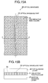
- Figs.15A-15B are figures for explaining a two-dimensional photonic crystal slab waveguide of the example 3-2.
- Fig.15A shows a top view of the optical waveguide
- Fig.15B shows an A-A' section view.
- a single line of the low refractive index columns 25 which exists in a part to become an optical waveguide part 22 is placed in a position moved by a half distance of the lattice constant of the square lattice from the normal lattice position in the optical propagation direction, in addition, the radius of the moved low refractive index columns is changed as necessary according to waveguide characteristics.
- the range of the radius of the low refractive index columns for providing the photonic crystal can be a range which allows existence of photonic band-gap. According to theoretical calculation by the plane wave expansion method, when the refractive index of the dielectric thin-film slab 21 is about from 3 to 4.5, and the refractive index of the other parts is about from 1 to 1.7, the radius of the low refractive index columns 25 is about from 0.35a to 0.45a.
- the two-dimensional photonic crystal slab waveguide of present invention is formed such that a part of holes in a lattice structure of a two-dimensional photonic crystal slab do not exist linearly so that a line defect is formed, and that a first width which is a distance between centers of nearest two lattice points located on both sides of the line defect is narrower than a second width which is a distance between centers of nearest two lattice points located on both sides of a line defect in a normal two-dimensional photonic crystal slab waveguide which simply lacks holes of a single line. Therefore, an optical waveguide which can form a single waveguiding mode having large group velocity below the light line can be provided.
- an optical waveguide which can form a single waveguiding mode having low loss above the light line can be provided.
- microminiaturized optical waveguide structure which improves group velocity and has small loss can be provided.
Landscapes
- Physics & Mathematics (AREA)
- Engineering & Computer Science (AREA)
- Optics & Photonics (AREA)
- Microelectronics & Electronic Packaging (AREA)
- General Physics & Mathematics (AREA)
- Chemical & Material Sciences (AREA)
- Nanotechnology (AREA)
- Life Sciences & Earth Sciences (AREA)
- Biophysics (AREA)
- Crystallography & Structural Chemistry (AREA)
- Optical Integrated Circuits (AREA)
Abstract
Description
Claims (19)
- A two-dimensional photonic crystal slab waveguide in which a part of holes in a lattice structure of a two-dimensional photonic crystal slab do not exist linearly so that a line defect is formed, characterized in that:a first width which is a distance between centers of nearest two lattice points located on both sides of said line defect is different from a second width which is a distance between centers of nearest two lattice points located on both sides of a line defect in a normal two-dimensional photonic crystal slab waveguide which simply lacks holes of a single line.
- The two-dimensional photonic crystal slab waveguide as claimed in claim 1, wherein said first width is a value from 0.5 times to 0.85 times of said second width.
- The two-dimensional photonic crystal slab waveguide as claimed in claim 1, said lattice structure is formed by air-hole triangle lattices.
- The two-dimensional photonic crystal slab waveguide as claimed in claim 2, said two-dimensional photonic crystal slab waveguide includes an oxide cladding or a polymer cladding.
- The two-dimensional photonic crystal slab waveguide as claimed in claim 4, wherein said two-dimensional photonic crystal slab waveguide is formed by using a Silicon-On-Insulator (SOI) substrate.
- The two-dimensional photonic crystal slab waveguide as claimed in claim 1, wherein said first width is wider than said second width in which a single-mode appears in a high frequency side of a light line of cladding in a dispersion relation of waveguiding modes of said two-dimensional photonic crystal slab waveguide having said first width.
- The two-dimensional photonic crystal slab waveguide as claimed in claim 6, wherein said first width is a value from 1.3 times to 1.6 times of said second width.
- The two-dimensional photonic crystal slab waveguide as claimed in claim 7, said lattice structure is formed by air-hole triangle lattices.
- The two-dimensional photonic crystal slab waveguide as claimed in claim 7, said two-dimensional photonic crystal slab waveguide includes an oxide cladding or a polymer cladding.
- The two-dimensional photonic crystal slab waveguide as claimed in claim 9, wherein said two-dimensional photonic crystal slab waveguide is formed by using a Silicon-On-Insulator (SOI) substrate.
- A two-dimensional photonic crystal slab waveguide in which dielectric cylindrical or polygon columns having lower refractive index than that of a dielectric thin-film slab are provided in said dielectric thin-film slab in a two-dimensional lattice pattern, and said dielectric thin-film slab is sandwiched by a top cladding layer and a bottom cladding layer which have lower refractive index than that of said dielectric thin-film slab, characterized in that:dielectric columns in an optical waveguide part in said two-dimensional photonic crystal slab waveguide are located at positions which are shifted in an optical propagation direction from positions at which said dielectric columns should be positioned in a normal two-dimensional photonic crystal slab.
- The two-dimensional photonic crystal slab waveguide as claimed in claim 11, wherein:a first diameter of said dielectric columns in said optical waveguide part is different from a second diameter of other dielectric columns located in parts other than said optical waveguide part, and said first diameter is a value by which said dielectric columns does not contact with said other dielectric columns.
- The two-dimensional photonic crystal slab waveguide as claimed in claim 11, wherein each dielectric column of dielectric columns in said optical waveguide part is apart from a position at which said each dielectric column should be positioned in said normal two-dimensional photonic crystal slab by a half of the lattice constant of said normal two-dimensional photonic crystal slab.
- The two-dimensional photonic crystal slab waveguide as claimed in claim 11, wherein said dielectric cylindrical or polygon columns are arranged in a triangle lattice pattern having a lattice constant "a", a radius or a half-breadth of said dielectric cylindrical or polygon columns is from 0.2a to 0.45a, and said radius or half-breadth is determined such that said dielectric cylindrical or polygon columns do not contact with dielectric columns in said optical waveguide part.
- The two-dimensional photonic crystal slab waveguide as claimed in claim 14, wherein:a refractive index of said dielectric thin-film slab is from 3.0 to 4.5, and each of refractive indices of parts other than said dielectric thin-film slab is from 1.0 to 1.7.
- The two-dimensional photonic crystal slab waveguide as claimed in claim 11, wherein said dielectric cylindrical or polygon columns are arranged in a square lattice pattern having a lattice constant "a", a radius or a half-breadth of said dielectric cylindrical or polygon columns is from 0.35a to 0.45a, and said radius or half-breadth is determined such that wherein said dielectric cylindrical or polygon columns do not contact with dielectric columns in said optical waveguide part.
- The two-dimensional photonic crystal slab waveguide as claimed in claim 16, wherein:a refractive index of said dielectric thin-film slab is from 3.0 to 4.5, and each of refractive indices of parts other than said dielectric thin-film slab is from 1.0 to 1.7.
- The two-dimensional photonic crystal slab waveguide as claimed in claim 11, wherein:silicon, germanium, gallium arsenide base compound, indium phosphide base compound, or indium antimony base compound is used as a material of said dielectric thin-film slab, and silica, polyimide base organic compound, epoxy base organic compound, acrylic base organic compound, air or vacuum is used as a material of parts other than said dielectric thin-film slab.
- The two-dimensional photonic crystal slab waveguide as claimed in claim 18, wherein said two-dimensional photonic crystal slab waveguide is formed by using a Silicon-On-Insulator (SOI) substrate.
Priority Applications (2)
| Application Number | Priority Date | Filing Date | Title |
|---|---|---|---|
| EP04028878A EP1512994B1 (en) | 2000-12-27 | 2001-12-21 | Photonic crystal waveguide |
| EP04028879A EP1512995B1 (en) | 2000-12-27 | 2001-12-21 | Photonic crystal waveguide |
Applications Claiming Priority (6)
| Application Number | Priority Date | Filing Date | Title |
|---|---|---|---|
| JP2000396962 | 2000-12-27 | ||
| JP2000396962 | 2000-12-27 | ||
| JP2001053634 | 2001-02-28 | ||
| JP2001053634 | 2001-02-28 | ||
| JP2001081919 | 2001-03-22 | ||
| JP2001081919 | 2001-03-22 |
Related Child Applications (2)
| Application Number | Title | Priority Date | Filing Date |
|---|---|---|---|
| EP04028879A Division EP1512995B1 (en) | 2000-12-27 | 2001-12-21 | Photonic crystal waveguide |
| EP04028878A Division EP1512994B1 (en) | 2000-12-27 | 2001-12-21 | Photonic crystal waveguide |
Publications (3)
| Publication Number | Publication Date |
|---|---|
| EP1219984A2 true EP1219984A2 (en) | 2002-07-03 |
| EP1219984A3 EP1219984A3 (en) | 2004-05-26 |
| EP1219984B1 EP1219984B1 (en) | 2007-07-11 |
Family
ID=27345563
Family Applications (3)
| Application Number | Title | Priority Date | Filing Date |
|---|---|---|---|
| EP04028878A Expired - Lifetime EP1512994B1 (en) | 2000-12-27 | 2001-12-21 | Photonic crystal waveguide |
| EP01310803A Expired - Lifetime EP1219984B1 (en) | 2000-12-27 | 2001-12-21 | Photonic crystal waveguide |
| EP04028879A Expired - Lifetime EP1512995B1 (en) | 2000-12-27 | 2001-12-21 | Photonic crystal waveguide |
Family Applications Before (1)
| Application Number | Title | Priority Date | Filing Date |
|---|---|---|---|
| EP04028878A Expired - Lifetime EP1512994B1 (en) | 2000-12-27 | 2001-12-21 | Photonic crystal waveguide |
Family Applications After (1)
| Application Number | Title | Priority Date | Filing Date |
|---|---|---|---|
| EP04028879A Expired - Lifetime EP1512995B1 (en) | 2000-12-27 | 2001-12-21 | Photonic crystal waveguide |
Country Status (3)
| Country | Link |
|---|---|
| US (1) | US6643439B2 (en) |
| EP (3) | EP1512994B1 (en) |
| DE (3) | DE60129286T2 (en) |
Cited By (8)
| Publication number | Priority date | Publication date | Assignee | Title |
|---|---|---|---|---|
| EP1380861A3 (en) * | 2002-07-10 | 2005-06-29 | Agilent Technologies Inc | waveguide in two dimensional slab photonic crystals with noncircular holes |
| DE102004024131A1 (en) * | 2004-05-14 | 2005-12-08 | Julius-Maximilians-Universität Würzburg | Waveguide for use as e.g. active conductor, has planar waveguide layer surrounded by cladding layers, where thickness value of waveguide layer is larger than wavelength of light in waveguide layer |
| EP1653261A1 (en) * | 2004-10-29 | 2006-05-03 | Ricoh Company, Ltd. | Optical control device including a photonic crystal waveguide |
| EP1589356A4 (en) * | 2003-01-31 | 2006-08-16 | Tdk Corp | Two-dimensional photonic crystal |
| EP1857845A1 (en) * | 2006-05-19 | 2007-11-21 | Ngk Insulators, Ltd. | Optical waveguide structures |
| EP1984768A1 (en) * | 2006-02-16 | 2008-10-29 | Hewlett-Packard Development Company, L.P. | Composite evanescent waveguides and associated methods |
| CN103176328A (en) * | 2013-04-11 | 2013-06-26 | 青岛大学 | Two-dimensional silicon substrate photonic crystal line-defect slow optical waveguide device |
| CN113922095A (en) * | 2021-09-18 | 2022-01-11 | 浙江大学 | Adjustable suction-permeation integrated conformal frequency selective surface |
Families Citing this family (56)
| Publication number | Priority date | Publication date | Assignee | Title |
|---|---|---|---|---|
| JP3846228B2 (en) * | 2001-06-07 | 2006-11-15 | 日本電気株式会社 | Waveguide |
| FR2832513B1 (en) * | 2001-11-21 | 2004-04-09 | Centre Nat Rech Scient | PHOTON CRYSTAL STRUCTURE FOR FASHION CONVERSION |
| JP3682289B2 (en) | 2002-12-06 | 2005-08-10 | 独立行政法人科学技術振興機構 | Two-dimensional photonic crystal optical multiplexer / demultiplexer using boundary reflection |
| WO2004113964A1 (en) * | 2003-06-19 | 2004-12-29 | Nec Corporation | Photonic crystal structure |
| US7016586B2 (en) * | 2003-06-20 | 2006-03-21 | Mesophotonics Limited | Optical waveguide structure |
| JP4761426B2 (en) * | 2003-07-25 | 2011-08-31 | 三菱電機株式会社 | Optical device and semiconductor laser oscillator |
| JP4538718B2 (en) | 2003-08-28 | 2010-09-08 | アルプス電気株式会社 | Two-dimensional photonic crystal slab and two-dimensional photonic crystal waveguide |
| US7283716B2 (en) * | 2003-10-21 | 2007-10-16 | The Regents Of The University Of Colorado | Strain tunable, flexible photonic crystals |
| US7251386B1 (en) | 2004-01-14 | 2007-07-31 | Luxtera, Inc | Integrated photonic-electronic circuits and systems |
| US7773836B2 (en) | 2005-12-14 | 2010-08-10 | Luxtera, Inc. | Integrated transceiver with lightpipe coupler |
| WO2005085921A1 (en) * | 2004-03-03 | 2005-09-15 | Japan Science And Technology Agency | Photonic crystal coupling defect waveguide and photonic crystal device |
| JP4208754B2 (en) * | 2004-03-24 | 2009-01-14 | 株式会社リコー | Optical delay element |
| CN100487503C (en) * | 2004-05-20 | 2009-05-13 | 松下电器产业株式会社 | Photonic crystal device |
| US7447404B2 (en) * | 2004-05-27 | 2008-11-04 | Energy Conversion Devices, Inc. | Photonic integrated circuit |
| WO2006014643A2 (en) * | 2004-07-20 | 2006-02-09 | The Trustees Of Columbia University In The City Of New York | Enhanced raman amplification and lasing in silicon-based photonic crystals |
| WO2006051942A1 (en) * | 2004-11-15 | 2006-05-18 | Matsushita Electric Industrial Co., Ltd. | Optical waveguide element |
| US7466424B2 (en) * | 2004-11-17 | 2008-12-16 | Ramot At Tel Aviv University Ltd. | Displacement sensor based on photonic crystal waveguides |
| US20090285522A1 (en) * | 2005-01-06 | 2009-11-19 | Nec Corporation | Optical waveguide, optical device, and optical communication device |
| US7532656B2 (en) | 2005-02-16 | 2009-05-12 | The Trustees Of Columbia University In The City Of New York | All-silicon raman amplifiers and lasers based on micro ring resonators |
| CN100434898C (en) * | 2005-04-30 | 2008-11-19 | 北京大学 | Two-dimensional photonic crystal humidity sensor and its realization method and preparation method |
| US7486849B2 (en) * | 2005-06-30 | 2009-02-03 | International Business Machines Corporation | Optical switch |
| US7869470B2 (en) * | 2005-08-31 | 2011-01-11 | The Trustees Of Columbia University In The City Of New York | Devices and methods for providing stimulated raman lasing |
| US7263262B1 (en) * | 2006-02-14 | 2007-08-28 | Coveytech, Llc | All-optical logic gates using nonlinear elements-claim set VI |
| US7394958B2 (en) * | 2006-02-14 | 2008-07-01 | Coveytech, Llc | All-optical logic gates using nonlinear elements-claim set II |
| US20070189703A1 (en) * | 2006-02-14 | 2007-08-16 | Coveytech, Llc | All-optical logic gates using nonlinear elements-claim set I |
| US7409131B2 (en) * | 2006-02-14 | 2008-08-05 | Coveytech, Llc | All-optical logic gates using nonlinear elements—claim set V |
| US7428359B2 (en) * | 2006-02-14 | 2008-09-23 | Coveytech, Llc | All-optical logic gates using nonlinear elements—claim set IV |
| US7664355B2 (en) * | 2006-02-14 | 2010-02-16 | Coveytech Llc | All-optical gates using nonlinear elements-claim set III |
| JP4769658B2 (en) * | 2006-07-31 | 2011-09-07 | キヤノン株式会社 | Resonator |
| JP4785194B2 (en) * | 2006-08-25 | 2011-10-05 | 日本碍子株式会社 | Method for manufacturing slab type two-dimensional photonic crystal structure |
| JP4936313B2 (en) * | 2006-08-25 | 2012-05-23 | 日本碍子株式会社 | Light modulation element |
| US7697588B2 (en) * | 2006-11-02 | 2010-04-13 | Canon Kabushiki Kaisha | Structure having photonic crystal and surface-emitting laser using the same |
| US8059924B1 (en) * | 2007-09-13 | 2011-11-15 | Lawrence Livermore National Security, Llc | Multiplexed photonic membranes and related detection methods for chemical and/or biological sensing applications |
| KR101423721B1 (en) * | 2007-10-09 | 2014-07-31 | 서울바이오시스 주식회사 | Laser diodes with nanopatterns and methods for making them |
| JP5191996B2 (en) * | 2007-12-06 | 2013-05-08 | パナソニック株式会社 | Planar illumination device and liquid crystal display device using the same |
| CN101458210B (en) * | 2007-12-12 | 2012-09-19 | 清华大学 | Refractivity sensor |
| US8682128B2 (en) * | 2008-08-21 | 2014-03-25 | International Business Machines Corporation | Optical waveguide with periodic sub-wavelength sized regions |
| US8947657B2 (en) | 2008-09-08 | 2015-02-03 | Lawrence Livermore National Security, Llc | Methods for isolation and viability assessment of biological organisms |
| US8830450B2 (en) | 2009-12-02 | 2014-09-09 | Lawrence Livermore National Security, Llc | Methods and systems for Raman and optical cross-interrogation in flow-through silicon membranes |
| US20110247676A1 (en) * | 2008-09-30 | 2011-10-13 | The Regents Of The University Of California | Photonic Crystal Solar Cell |
| US8061573B2 (en) * | 2009-05-04 | 2011-11-22 | Campbell Hausfeld | Mode switch for fastener driving tool |
| US8786852B2 (en) * | 2009-12-02 | 2014-07-22 | Lawrence Livermore National Security, Llc | Nanoscale array structures suitable for surface enhanced raman scattering and methods related thereto |
| US20120154168A1 (en) * | 2010-12-16 | 2012-06-21 | Baker Hughes Incorporated | Photonic crystal waveguide downhole communication system and method |
| US9110316B2 (en) * | 2011-12-01 | 2015-08-18 | Samsung Electronics Co., Ltd. | Method of amplifying magneto-optical kerr effect by using photon crystal structures, and photon crystal having amplified magneto-optical kerr effect, method of fabricating photon crystal |
| US9395304B2 (en) | 2012-03-01 | 2016-07-19 | Lawrence Livermore National Security, Llc | Nanoscale structures on optical fiber for surface enhanced Raman scattering and methods related thereto |
| US9360620B2 (en) | 2012-08-29 | 2016-06-07 | Aurrion, Inc. | Thermal management for photonic integrated circuits |
| US9509122B1 (en) * | 2012-08-29 | 2016-11-29 | Aurrion, Inc. | Optical cladding layer design |
| CN102914819A (en) * | 2012-10-25 | 2013-02-06 | 浙江大学 | One-dimensional photonic crystal optical micro-cavity based on waveguide comprising low-refractive-index cores |
| US9042418B2 (en) | 2013-02-11 | 2015-05-26 | California Institute Of Technology | III-V photonic crystal microlaser bonded on silicon-on-insulator |
| CN110007398B (en) * | 2019-04-30 | 2020-11-03 | 江苏大学 | Optical waveguide for realizing photonic spin-guiding mechanism of topological boundary state in photonic crystals |
| CN110161621B (en) * | 2019-04-30 | 2020-11-03 | 江苏大学 | Photonic crystal slow light waveguide based on honeycomb structure |
| CN111045145B (en) * | 2019-12-25 | 2023-12-15 | 易锐光电科技(安徽)有限公司 | Thin film optical waveguide and method for manufacturing the same |
| CN113419303B (en) * | 2021-06-11 | 2022-06-14 | 太原理工大学 | A two-dimensional hexagonal boron nitride valley photonic crystal unidirectional light transmission structure |
| CN115291324B (en) * | 2022-07-08 | 2023-05-26 | 中国地质大学(武汉) | A silicon-based all-photodiode |
| CN116908961B (en) * | 2023-07-24 | 2025-10-17 | 中国地质大学(武汉) | Suspension groove zigzag one-dimensional photonic crystal |
| US12527112B2 (en) | 2023-08-30 | 2026-01-13 | Ciena Corporation | Managing optical shielding for integrated circuits |
Family Cites Families (13)
| Publication number | Priority date | Publication date | Assignee | Title |
|---|---|---|---|---|
| US5784400A (en) * | 1995-02-28 | 1998-07-21 | Massachusetts Institute Of Technology | Resonant cavities employing two dimensionally periodic dielectric materials |
| DE19720784A1 (en) * | 1997-05-17 | 1998-11-26 | Deutsche Telekom Ag | Integrated optical circuit |
| US6130969A (en) * | 1997-06-09 | 2000-10-10 | Massachusetts Institute Of Technology | High efficiency channel drop filter |
| US5999308A (en) * | 1998-04-01 | 1999-12-07 | Massachusetts Institute Of Technology | Methods and systems for introducing electromagnetic radiation into photonic crystals |
| EP0964305A1 (en) * | 1998-06-08 | 1999-12-15 | Corning Incorporated | Method of making a photonic crystal |
| US6134043A (en) * | 1998-08-11 | 2000-10-17 | Massachusetts Institute Of Technology | Composite photonic crystals |
| US6175671B1 (en) * | 1998-10-01 | 2001-01-16 | Nortel Networks Limited | Photonic crystal waveguide arrays |
| JP3456166B2 (en) * | 1999-06-23 | 2003-10-14 | 日本電気株式会社 | Optical coupling element and optical coupling method using photonic crystal |
| US6468823B1 (en) * | 1999-09-30 | 2002-10-22 | California Institute Of Technology | Fabrication of optical devices based on two dimensional photonic crystal structures and apparatus made thereby |
| JP3925769B2 (en) * | 2000-03-24 | 2007-06-06 | 関西ティー・エル・オー株式会社 | Two-dimensional photonic crystal and multiplexer / demultiplexer |
| US6597851B2 (en) * | 2000-08-09 | 2003-07-22 | Massachusetts Institute Of Technology | Periodic dielectric structure having a complete three-dimensional photonic band gap |
| EP1315987A4 (en) * | 2000-08-15 | 2005-06-29 | Corning Inc | Active photonic crystal waveguide device |
| US6532326B1 (en) * | 2000-09-21 | 2003-03-11 | Ut-Battelle, Llc | Transverse-longitudinal integrated resonator |
-
2001
- 2001-12-21 DE DE60129286T patent/DE60129286T2/en not_active Expired - Lifetime
- 2001-12-21 EP EP04028878A patent/EP1512994B1/en not_active Expired - Lifetime
- 2001-12-21 DE DE60127729T patent/DE60127729T2/en not_active Expired - Lifetime
- 2001-12-21 EP EP01310803A patent/EP1219984B1/en not_active Expired - Lifetime
- 2001-12-21 EP EP04028879A patent/EP1512995B1/en not_active Expired - Lifetime
- 2001-12-21 DE DE60127730T patent/DE60127730T2/en not_active Expired - Lifetime
- 2001-12-26 US US10/033,766 patent/US6643439B2/en not_active Expired - Lifetime
Cited By (15)
| Publication number | Priority date | Publication date | Assignee | Title |
|---|---|---|---|---|
| EP1380861A3 (en) * | 2002-07-10 | 2005-06-29 | Agilent Technologies Inc | waveguide in two dimensional slab photonic crystals with noncircular holes |
| US7477819B2 (en) | 2003-01-31 | 2009-01-13 | Tdk Corporation | Two-dimensional photonic crystal |
| EP1589356A4 (en) * | 2003-01-31 | 2006-08-16 | Tdk Corp | Two-dimensional photonic crystal |
| DE102004024131A1 (en) * | 2004-05-14 | 2005-12-08 | Julius-Maximilians-Universität Würzburg | Waveguide for use as e.g. active conductor, has planar waveguide layer surrounded by cladding layers, where thickness value of waveguide layer is larger than wavelength of light in waveguide layer |
| DE102004024131B4 (en) * | 2004-05-14 | 2007-04-12 | Julius-Maximilians-Universität Würzburg | Waveguide based on photonic crystals |
| US7215861B2 (en) | 2004-10-29 | 2007-05-08 | Ricoh Company, Ltd. | Optical control device |
| US7369734B2 (en) | 2004-10-29 | 2008-05-06 | Ricoh Company, Ltd. | Optical control device |
| EP1653261A1 (en) * | 2004-10-29 | 2006-05-03 | Ricoh Company, Ltd. | Optical control device including a photonic crystal waveguide |
| US7660506B2 (en) | 2005-05-19 | 2010-02-09 | Ngk Insulators, Ltd. | Optical waveguide structures |
| EP1984768A1 (en) * | 2006-02-16 | 2008-10-29 | Hewlett-Packard Development Company, L.P. | Composite evanescent waveguides and associated methods |
| EP1857845A1 (en) * | 2006-05-19 | 2007-11-21 | Ngk Insulators, Ltd. | Optical waveguide structures |
| CN103176328A (en) * | 2013-04-11 | 2013-06-26 | 青岛大学 | Two-dimensional silicon substrate photonic crystal line-defect slow optical waveguide device |
| CN103176328B (en) * | 2013-04-11 | 2015-04-08 | 青岛大学 | Two-dimensional silicon substrate photonic crystal line-defect slow optical waveguide device |
| CN113922095A (en) * | 2021-09-18 | 2022-01-11 | 浙江大学 | Adjustable suction-permeation integrated conformal frequency selective surface |
| CN113922095B (en) * | 2021-09-18 | 2022-11-29 | 浙江大学 | Adjustable suction-permeation integrated conformal frequency selective surface |
Also Published As
| Publication number | Publication date |
|---|---|
| DE60127730T2 (en) | 2007-12-27 |
| DE60127730D1 (en) | 2007-05-16 |
| US20020118941A1 (en) | 2002-08-29 |
| EP1512995B1 (en) | 2007-04-04 |
| EP1512994A1 (en) | 2005-03-09 |
| US6643439B2 (en) | 2003-11-04 |
| EP1512994B1 (en) | 2007-04-04 |
| EP1219984A3 (en) | 2004-05-26 |
| DE60129286D1 (en) | 2007-08-23 |
| DE60127729T2 (en) | 2007-12-27 |
| EP1512995A1 (en) | 2005-03-09 |
| DE60129286T2 (en) | 2007-11-22 |
| EP1219984B1 (en) | 2007-07-11 |
| DE60127729D1 (en) | 2007-05-16 |
Similar Documents
| Publication | Publication Date | Title |
|---|---|---|
| US6643439B2 (en) | Photonic crystal waveguide | |
| KR100578683B1 (en) | Optical device and its manufacturing method | |
| Atsushi Sakai et al. | Propagation characteristics of ultrahigh-Δ optical waveguide on silicon-on-insulator substrate | |
| Jamois et al. | Silicon-based two-dimensional photonic crystal waveguides | |
| Dideban et al. | Photonic crystal channel drop filter based on ring-shaped defects for DWDM systems | |
| US6728457B2 (en) | Waveguides in two dimensional slab photonic crystals with noncircular holes | |
| US7116878B2 (en) | Optical waveguide structure | |
| US7215861B2 (en) | Optical control device | |
| JP3800088B2 (en) | Photonic crystal waveguide | |
| Tokushima et al. | Light propagation in a photonic-crystal-slab line-defect waveguide | |
| US20160202414A1 (en) | Systems And Methods For Suspended Polymer Photonic Crystal Cavities And Waveguides | |
| Hadley | Out-of-plane losses of line-defect photonic crystal waveguides | |
| JP3867848B2 (en) | Optical waveguide | |
| Begović et al. | Manufacture reliability assessment of Si photonic foundry fabricated slow-light photonic crystal waveguides | |
| JP4062308B2 (en) | Photonic crystal waveguide | |
| JP4313344B2 (en) | Photonic crystal waveguide | |
| Brosi | Slow-light photonic crystal devices for high-speed optical signal processing | |
| Begovic et al. | Manufacture Reliability of Si Photonic Foundry Fabricated Slow-Light Photonic Crystal Waveguides | |
| Biswas et al. | Dirac‐mode guidance in silica‐based hollow‐core photonic crystal fiber with high‐index dielectric rings | |
| Kappeler et al. | Loss-relevant structural imperfections in substrate-type photonic crystal waveguides | |
| Deyasi | Computation of Electromagnetic Bandgap in Two-Dimensional Photonic Crystal | |
| Shinya et al. | Single-mode transmission in commensurate width-varied line-defect SOI photonic crystal waveguides | |
| Ma et al. | Low crosstalk waveguide intersections in honeycomb lattice photonic crystals for TM-polarized light | |
| O’Faolain | Photonic crystal cavities for optical interconnects | |
| Lu et al. | Single Mode Two Dimensional Photonic Crystal Waveguide on Thin Film Lithium Niobate |
Legal Events
| Date | Code | Title | Description |
|---|---|---|---|
| PUAI | Public reference made under article 153(3) epc to a published international application that has entered the european phase |
Free format text: ORIGINAL CODE: 0009012 |
|
| 17P | Request for examination filed |
Effective date: 20020115 |
|
| AK | Designated contracting states |
Kind code of ref document: A2 Designated state(s): AT BE CH CY DE DK ES FI FR GB GR IE IT LI LU MC NL PT SE TR |
|
| AX | Request for extension of the european patent |
Free format text: AL;LT;LV;MK;RO;SI |
|
| PUAL | Search report despatched |
Free format text: ORIGINAL CODE: 0009013 |
|
| AK | Designated contracting states |
Kind code of ref document: A3 Designated state(s): AT BE CH CY DE DK ES FI FR GB GR IE IT LI LU MC NL PT SE TR |
|
| AX | Request for extension of the european patent |
Extension state: AL LT LV MK RO SI |
|
| 17Q | First examination report despatched |
Effective date: 20040713 |
|
| AKX | Designation fees paid |
Designated state(s): DE FR GB |
|
| GRAP | Despatch of communication of intention to grant a patent |
Free format text: ORIGINAL CODE: EPIDOSNIGR1 |
|
| GRAS | Grant fee paid |
Free format text: ORIGINAL CODE: EPIDOSNIGR3 |
|
| GRAA | (expected) grant |
Free format text: ORIGINAL CODE: 0009210 |
|
| AK | Designated contracting states |
Kind code of ref document: B1 Designated state(s): DE FR GB |
|
| REG | Reference to a national code |
Ref country code: GB Ref legal event code: FG4D |
|
| REF | Corresponds to: |
Ref document number: 60129286 Country of ref document: DE Date of ref document: 20070823 Kind code of ref document: P |
|
| ET | Fr: translation filed | ||
| PLBE | No opposition filed within time limit |
Free format text: ORIGINAL CODE: 0009261 |
|
| STAA | Information on the status of an ep patent application or granted ep patent |
Free format text: STATUS: NO OPPOSITION FILED WITHIN TIME LIMIT |
|
| 26N | No opposition filed |
Effective date: 20080414 |
|
| REG | Reference to a national code |
Ref country code: FR Ref legal event code: PLFP Year of fee payment: 15 |
|
| REG | Reference to a national code |
Ref country code: FR Ref legal event code: PLFP Year of fee payment: 16 |
|
| REG | Reference to a national code |
Ref country code: FR Ref legal event code: PLFP Year of fee payment: 17 |
|
| PGFP | Annual fee paid to national office [announced via postgrant information from national office to epo] |
Ref country code: FR Payment date: 20201223 Year of fee payment: 20 Ref country code: GB Payment date: 20201223 Year of fee payment: 20 Ref country code: DE Payment date: 20201211 Year of fee payment: 20 |
|
| REG | Reference to a national code |
Ref country code: DE Ref legal event code: R071 Ref document number: 60129286 Country of ref document: DE |
|
| REG | Reference to a national code |
Ref country code: GB Ref legal event code: PE20 Expiry date: 20211220 |
|
| PG25 | Lapsed in a contracting state [announced via postgrant information from national office to epo] |
Ref country code: GB Free format text: LAPSE BECAUSE OF EXPIRATION OF PROTECTION Effective date: 20211220 |