EP1217725A1 - Monolithic integrated microwave voltage level shifting diode especially for microwave broadband optoelectronic transmitter - Google Patents
Monolithic integrated microwave voltage level shifting diode especially for microwave broadband optoelectronic transmitter Download PDFInfo
- Publication number
- EP1217725A1 EP1217725A1 EP01403225A EP01403225A EP1217725A1 EP 1217725 A1 EP1217725 A1 EP 1217725A1 EP 01403225 A EP01403225 A EP 01403225A EP 01403225 A EP01403225 A EP 01403225A EP 1217725 A1 EP1217725 A1 EP 1217725A1
- Authority
- EP
- European Patent Office
- Prior art keywords
- circuit
- diode
- voltage
- offset
- downstream
- Prior art date
- Legal status (The legal status is an assumption and is not a legal conclusion. Google has not performed a legal analysis and makes no representation as to the accuracy of the status listed.)
- Withdrawn
Links
Images


Classifications
-
- H—ELECTRICITY
- H03—ELECTRONIC CIRCUITRY
- H03F—AMPLIFIERS
- H03F3/00—Amplifiers with only discharge tubes or only semiconductor devices as amplifying elements
- H03F3/60—Amplifiers in which coupling networks have distributed constants, e.g. with waveguide resonators
- H03F3/605—Distributed amplifiers
- H03F3/607—Distributed amplifiers using FET's
-
- H—ELECTRICITY
- H03—ELECTRONIC CIRCUITRY
- H03F—AMPLIFIERS
- H03F1/00—Details of amplifiers with only discharge tubes, only semiconductor devices or only unspecified devices as amplifying elements
- H03F1/08—Modifications of amplifiers to reduce detrimental influences of internal impedances of amplifying elements
- H03F1/18—Modifications of amplifiers to reduce detrimental influences of internal impedances of amplifying elements by use of distributed coupling, i.e. distributed amplifiers
-
- H—ELECTRICITY
- H03—ELECTRONIC CIRCUITRY
- H03F—AMPLIFIERS
- H03F3/00—Amplifiers with only discharge tubes or only semiconductor devices as amplifying elements
- H03F3/04—Amplifiers with only discharge tubes or only semiconductor devices as amplifying elements with semiconductor devices only
- H03F3/08—Amplifiers with only discharge tubes or only semiconductor devices as amplifying elements with semiconductor devices only controlled by light
- H03F3/085—Amplifiers with only discharge tubes or only semiconductor devices as amplifying elements with semiconductor devices only controlled by light using opto-couplers between stages
Definitions
- the present invention relates to a shift diode in voltage realized in integrated microwave monolithic technology.
- Said offset diode is intended to ensure a voltage offset between two circuits including the downstream circuit consumes a relatively high bias current.
- the downstream circuit is an optoelectronic transmitter very broadband microwave, from a few Hz to several GHz, such as a laser diode.
- MMIC Monolithic Microwave Integrated Circuit
- a distributed amplifier (simple or transimpedance) has a plurality of amplifying cells basic, mounted between an input line and a line Release.
- Each basic amplifier cell has at least minus a field effect transistor, bipolar, or the like.
- each transistor is connected to the common drain line (outlet line) through its drain as well than to the common grid line (entry line) by its wire rack.
- the description will be limited to field effect transistors, but the skilled person knows that he can easily transpose the present invention to bipolar transistors or the like.
- the polarization filter circuits must let pass the DC bias voltages or currents and isolate the microwave power.
- the power supply terminal which receives the bias voltage from the drains of transistors is connected to the common drain line across bias resistance and decoupling ability in parallel connected to ground.
- the terminal which receives the bias voltage of transistor grids is connected to the grid line common across a bias resistor and a parallel decoupling capacity connected to ground.
- a link capacity is provided between the line of drains common, which forms the output of the distributed amplifier, and the anode of the laser diode.
- Such a link capacity isolates microwave power of continuous polarization.
- connection capacity by high-value capacity mounted outside the circuit cannot be considered here to increase the impedance of bonding capacity.
- a bonding capacity is placed between two non-zero voltage points, which prevents mounting of a capacity outside the integrated circuit (MMIC chip).
- the present invention provides a solution to this problem.
- It relates to an interface device between two circuits, the upstream circuit of which comprises an outlet and means for DC voltage polarization, and the downstream circuit includes input, uses DC bias voltage of higher value than that of the upstream circuit and consumes a relatively large bias current which is a function of the power delivered by the circuit downstream.
- the device interface includes a voltage offset diode mounted between the output of the upstream circuit and the input of the downstream circuit, the characteristic of the shift diode being chosen from so that the bias voltage of the upstream circuit either offset by an offset corresponding substantially to the difference between the bias voltages of the upstream circuits and downstream and whose value corresponds substantially to the threshold voltage of the shift diode, and the current of polarization of the downstream circuit being relatively large by relation to the threshold current of the shift diode.
- Such an offset diode eliminates the capacitance of connection between the upstream and downstream circuits, which makes said downstream circuit capable of operating over a very wide frequency band from a few Hz to several GHz.
- the bridge at diodes is used in a feedback loop in which passes a relatively weak current, substantially equal to the threshold current of the elementary diodes of the bridge at diodes.
- the shift diode comprises a plurality of transistors made in monolithic integrated technology microwave and mounted in parallel between the output of the upstream circuit and the input of the downstream circuit.
- each shift diode transistor includes a drain and a source connected to each other, each grid finger forming a diode effect contact.
- the downstream circuit includes a laser diode capable of emitting very broadband microwave signals.
- the upstream circuit includes a control circuit of the 50 ohm impedance laser diode and an amplifier distributed power acting as a low adapter impedance.
- the designs contain elements of a certain character. AT as such they can not only serve to do better understand the invention but also to contribute to the definition if necessary.
- the link uses direct amplitude modulation.
- the emitting head 4 comprises a laser diode 8 whose current is modulated by the radio frequency and microwave signal incident 12.
- the emitting head 4 comprises a device for polarization 10, if necessary a pre-amplification stage 14, and an impedance amplification and adaptation stage 16.
- the role of stage 16 is to adapt between the low impedance of the laser diode (around 10 ohms) and the classical impedance (50 ohms) of the input device (command) of the laser diode.
- a photodiode 20 picks up the signals transmitted by optical fiber 2.
- the receiving head 6 also includes an impedance matching stage 22, the if necessary a pre-amplification stage 24, and a device polarization of the photodiode 26.
- the output 28 of the receiving head can deliver a microwave signal at very broadband ranging from a few Hz to several GHz.
- stage 16 includes an amplifier distributed 18 says transimpedance playing the role of amplifier and low impedance adapter for the laser diode 8.
- the distributed amplifier 18 comprises a plurality of base amplifying cells AB, mounted between an input line (common line of drains LD in the case of field effect transistors mounted in common source) and an output line (LG common grid line).
- Each basic amplifier cell AB has at least one TEF field effect transistor mounted in common O source and connected to the common line of drains LD by its drain D as well than to the common grid line LG by its grid G.
- the BG supply terminal which receives the voltage of polarization VG of the gates of the transistors is connected to the common grid line LG through a resistor RG (from about 1 Kiloohms for example) and a capacity of decoupling CG in parallel connected to ground.
- Sons inductance IG1 and IG2 connect the power supply delivering the VG voltage at terminal BG.
- the common line of drains LD is polarized in voltage VD via a power supply filter circuit PD connected to the power supply terminal BD through inductors ID1, ID2 and ID3 and decoupling capacities CD1 and CD2 in parallel and connected to ground.
- the output S of the distributed amplifier 18 is connected to the anode 11 of the laser diode 8 through a ribbon or wire 17.
- the cathode 13 of the laser diode 8 is connected to ground.
- the laser diode 8 is biased at a bias voltage continues VL through an inductor 15, for example from around 15nH.
- the current of the laser diode 8 is of the order of 150 mA and the voltage of the laser diode 8 is around 1.4 volts.
- CL connection capacity is provided according to the prior art between the end of the common line of drains LD which forms the output S of the distributed amplifier and the anode 11 of the laser diode 8 (via ribbon 17).
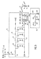
- the amplifier is shown distributed 18 described with reference to FIG. 2 in which has in particular replaced the CL capacitance by a diode DD offset according to the invention.
- the DD voltage offset diode is mounted between the end 32 of an inductor 34 forming the output S of the amplifier distributed 18 and the anode 11 of the laser diode 8 to through the wire or ribbon 17.
- the shift diode comprises a plurality of transistors made in monolithic microwave technology broadband and mounted in parallel between the outlet of the upstream circuit and the input of the downstream circuit.
- each transistor of the shift diode includes a drain and a source connected to each other, which forms an elementary diode DE.
- the DD shift diode includes for example two rows RA1 and RA2 of elementary diodes DE connected in parallel between the amplifier output distributed and the laser diode.
- the first row RA1 of elementary diodes DE comprises n individualized diodes in DE11 to DE1n, with for example n equal to 74 and the second row RA2 of elementary diodes includes n individualized diodes in DE21 to DE2n, with by example n equal to 74.
- the elementary diodes are arranged according to a arrangement in which the node 30-1 is connected in series to the output (here the end of inductance 34) of the amplifier distributed, and in parallel with the anode of the diode DE11 and at the anode of the diode DE21.
- node 30-2 is connected in series to node 30-1, and in parallel to the anode of the diode DE12 and the anode of diode DE22.
- the knot 30-n is connected in series to node 30-n-1, and in parallel with the anode of the diode DE1n and the anode of the diode DE2n.
- the cathodes of the elementary diodes DE are connected to the node 40 intended to be connected to the anode of the laser diode 8, via the ribbon 17 (if applicable).
- the 30-n node can advantageously play the power supply terminal which receives the bias voltage VD from the line of common drains LD through the filter circuit PD described with reference to Figure 2.
- the filtering circuit PD can also play the role of filtering the bias voltage VL of the laser diode 8, which eliminates the inductance 15 described with reference to Figure 2.
- CQ of the DD offset diode which gives the voltage continuous VL (in volts) across the offset diode DD as a function of the intensity ID (in amperes) passing through it.
- the DD offset diode is chosen so that the bias voltage VD of the common drain line LD either offset by an offset corresponding substantially to the difference between the bias voltage VD of the line of common drains LD and the bias voltage VL of the laser diode.
- the operating point PF of the diode of offset is chosen equal to 1.1 V with maximum intensity of 164 mA and the SL threshold of the diode offset is chosen equal to 0.925 V with an intensity 11 mA minimum.
- the threshold current (here 11 mA) of the offset diode is therefore relatively small compared to the current consumed by the downstream circuit (here 164 mA).
- the voltage offset is thus of the order of 1.1 V, which roughly corresponds to the operating point value PF of the DD offset diode.
- laser diode 8 Due to the removal of CL link capacity between the upstream 16 and downstream 8 circuits and its replacement by DD shift diode, laser diode 8 can work in a very wide frequency band ranging for example from a few Hz to several GHz.
- the PS circuit includes a plurality of transistors additional TS operating at saturable load.
- the SS sources of additional TS transistors are distributively connected to the common line of drains LD.
- the DS drains of the additional TS transistors receive series the bias voltage VD.
- the GS grids of the additional transistors receive in series a second VG2 gate bias voltage, the if necessary respectively through additional resistance RS.
- the voltage VG2 is connected to ground in parallel through a CSS decoupling capacity.
- each additional grid is linked to its source respective through additional capacity CS.
- the PS circuit remedies the drawbacks (energy loss, congestion) resulting from the filtering of the polarization across RG terminal resistors like that described with reference to Figure 2.
- the PS circuit remedies the disadvantages (degradations performance, impedance mismatch, resonance, dimensions, welds) resulting from the filtering of the polarization through inductive elements 15, ID1, ID2, ID3 like those described with reference to Figures 2 and / or 3.
- the shift diode DD comprises for example two rows RA1 and RA2 of n transistors. Each transistor forms a diode elementary DE by connecting its drain to its source.
- Each transistor includes a DG gate finger, individualized in DG11 to DG1n for the first row RA1 and in DG21 to DG2n for the second row RA2.
- Each gate finger DG of the diode DD is produced according to a contact called "Schottky” SK similar to the transistor grids field effect.
- a “Schottky” SK contact is a metal / semiconductor contact that results in a AC potential barrier. Such a “Schottky” contact presents a diode effect.
- the drains and the sources of the transistors of the shift diode are made according to a so-called "ohmic" contact OH which is a metal / semiconductor contact requiring a more complex metallurgy than that of the Schottky contact SK.
- ohmic contact generally involves materials of the Germanium, Gold, or Gallium Arsenide type, and results in the absence of a potential barrier. So it's a contact without diode effect with low resistance value.
- the intermediate zone AC between the ohmic contact and the Schottky contact is an active area.
- Each grid finger has an individual development of around 5 micrometers. So the shift diode has a total grid development of the order of 148 x 5 micrometers, or of the order of 740 micrometers.
- FIG 7 there is shown a mask which illustrates the construction of circuit 16 described with reference to Figure 3 and which includes a distributed amplifier 18 according to the invention and a DD shift diode.
Abstract
Description
La présente invention concerne une diode de décalage en tension réalisée en technologie intégrée monolithique hyperfréquence. Ladite diode de décalage est destinée à assurer un décalage en tension entre deux circuits dont le circuit aval consomme un courant de polarisation relativement élevé. Par exemple, le circuit aval est un émetteur optoélectronique hyperfréquence à très large bande, allant de quelques Hz à plusieurs GHz, telle qu'une diode laser.The present invention relates to a shift diode in voltage realized in integrated microwave monolithic technology. Said offset diode is intended to ensure a voltage offset between two circuits including the downstream circuit consumes a relatively high bias current. Through example, the downstream circuit is an optoelectronic transmitter very broadband microwave, from a few Hz to several GHz, such as a laser diode.
Elle trouve une application générale dans la fabrication de circuits intégrés monolithiques hyperfréquences, appelés encore MMIC pour "Monolithic Microwave Integrated Circuit", et plus particulièrement en optoélectronique, dans la transmission de signaux hyperfréquences sur fibres optiques.It finds general application in the manufacture of monolithic microwave integrated circuits, called again MMIC for "Monolithic Microwave Integrated Circuit", and more particularly in optoelectronics, in transmission microwave signals on optical fibers.
On connaít déjà des émetteurs optoélectroniques du type diode laser émettant des signaux hyperfréquence à très large bande.We already know optoelectronic emitters of the diode type laser emitting very wide band microwave signals.
Par exemple, dans le brevet FR 96 04 524, un amplificateur distribué dit transimpédance joue le rôle d'amplificateur et d'adaptateur basse impédance pour une diode laser émettant des signaux hyperfréquence à très large bande.For example, in patent FR 96 04 524, an amplifier distributed says transimpedance plays the role of amplifier and low impedance adapter for an emitting laser diode very wideband microwave signals.
D'une manière générale, un amplificateur distribué (simple ou transimpédance) comporte une pluralité de cellules amplificatrices de base, montées entre une ligne d'entrée et une ligne de sortie. Chaque cellule amplificatrice de base comporte au moins un transistor à effet de champ, bipolaire, ou analogue. Par exemple, dans le cas de transistors à effet de champ montés en source commune, chaque transistor est relié à la ligne de drains commune (ligne de sortie) par son drain ainsi qu'à la ligne de grille commune (ligne d'entrée) par sa grille. Par la suite, on limitera la description à des transistors à effet de champ, mais l'homme du métier sait qu'il pourra transposer sans difficultés la présente invention à des transistors bipolaires ou analogues.Generally speaking, a distributed amplifier (simple or transimpedance) has a plurality of amplifying cells basic, mounted between an input line and a line Release. Each basic amplifier cell has at least minus a field effect transistor, bipolar, or the like. For example, in the case of field effect transistors mounted as a common source, each transistor is connected to the common drain line (outlet line) through its drain as well than to the common grid line (entry line) by its wire rack. Thereafter, the description will be limited to field effect transistors, but the skilled person knows that he can easily transpose the present invention to bipolar transistors or the like.
Le fonctionnement correct d'un transistor à effet de champ nécessite l'application d'une tension de polarisation continue sur son drain, et l'application d'une tension de polarisation continue sur sa grille.The correct operation of a field effect transistor requires the application of a bias voltage continues on its drain, and the application of a voltage of continuous polarization on its grid.
En pratique, les circuits de filtrage de polarisation doivent laisser passer les tensions ou courants continus de polarisation et isoler la puissance hyperfréquence. A cet effet, (notamment dans le brevet FR 96 04 524), la borne d'alimentation qui reçoit la tension de polarisation des drains des transistors est reliée à la ligne de drains commune à travers une résistance de polarisation et une capacité de découplage en parallèle reliée à la masse. De son côté, la borne d'alimentation qui reçoit la tension de polarisation des grilles des transistors est reliée à la ligne de grille commune à travers une résistance de polarisation et une capacité de découplage en parallèle reliée à la masse.In practice, the polarization filter circuits must let pass the DC bias voltages or currents and isolate the microwave power. To this end, (in particular in patent FR 96 04 524), the power supply terminal which receives the bias voltage from the drains of transistors is connected to the common drain line across bias resistance and decoupling ability in parallel connected to ground. For its part, the terminal which receives the bias voltage of transistor grids is connected to the grid line common across a bias resistor and a parallel decoupling capacity connected to ground.
De plus, (comme dans le brevet FR mentionné ci-avant), une capacité de liaison est prévue entre la ligne de drains commune, qui forme la sortie de l'amplificateur distribué, et l'anode de la diode laser.In addition, (as in the FR patent mentioned above), a link capacity is provided between the line of drains common, which forms the output of the distributed amplifier, and the anode of the laser diode.
Une telle capacité de liaison isole la puissance hyperfréquence de la polarisation continue.Such a link capacity isolates microwave power of continuous polarization.
Mais une telle capacité de liaison empêche aussi le passage des basses fréquences, par exemple celles inférieures à 500 MHz, que demandent certaines applications de transmission de signaux hyperfréquences.But such a bonding capacity also prevents the passage low frequencies, for example those below 500 MHz, which certain transmission applications require microwave signals.
La solution consistant à compléter la capacité de liaison par une capacité de forte valeur montée à l'extérieur du circuit ne peut pas être envisagée ici pour augmenter l'impédance de la capacité de liaison. En effet, contrairement à une capacité de découplage dont l'une des armatures est reliée à la masse, une capacité de liaison est placée entre deux points de tension non nulle, ce qui empêche le montage d'une capacité extérieure au circuit intégré (puce MMIC).The solution consisting in supplementing the connection capacity by high-value capacity mounted outside the circuit cannot be considered here to increase the impedance of bonding capacity. In fact, unlike a decoupling capacity of which one of the reinforcements is connected to ground, a bonding capacity is placed between two non-zero voltage points, which prevents mounting of a capacity outside the integrated circuit (MMIC chip).
La présente invention apporte une solution à ce problème.The present invention provides a solution to this problem.
Elle porte sur un dispositif d'interface entre deux circuits, dont le circuit amont comprend une sortie et des moyens de polarisation en tension continue, et dont le circuit aval comprend une entrée, utilise une tension continue de polarisation de valeur plus élevée que celle du circuit amont et consomme un courant de polarisation relativement important qui est fonction de la puissance délivrée par le circuit aval.It relates to an interface device between two circuits, the upstream circuit of which comprises an outlet and means for DC voltage polarization, and the downstream circuit includes input, uses DC bias voltage of higher value than that of the upstream circuit and consumes a relatively large bias current which is a function of the power delivered by the circuit downstream.
Selon une définition générale de l'invention, le dispositif d'interface comprend une diode de décalage en tension montée entre la sortie du circuit amont et l'entrée du circuit aval, la caractéristique de la diode de décalage étant choisie de telle sorte que la tension de polarisation du circuit amont soit décalée d'un décalage correspondant sensiblement à l'écart entre les tensions de polarisation des circuits amont et aval et dont la valeur correspond sensiblement à la tension de seuil de la diode de décalage, et le courant de polarisation du circuit aval étant relativement important par rapport au courant de seuil de la diode de décalage.According to a general definition of the invention, the device interface includes a voltage offset diode mounted between the output of the upstream circuit and the input of the downstream circuit, the characteristic of the shift diode being chosen from so that the bias voltage of the upstream circuit either offset by an offset corresponding substantially to the difference between the bias voltages of the upstream circuits and downstream and whose value corresponds substantially to the threshold voltage of the shift diode, and the current of polarization of the downstream circuit being relatively large by relation to the threshold current of the shift diode.
Une telle diode de décalage permet de supprimer la capacité de liaison entre les circuits amont et aval, ce qui rend ledit circuit aval apte à fonctionner dans une très large bande de fréquence allant de quelques Hz à plusieurs GHz.Such an offset diode eliminates the capacitance of connection between the upstream and downstream circuits, which makes said downstream circuit capable of operating over a very wide frequency band from a few Hz to several GHz.
Même si on connaít déjà des diodes réalisées en technologie intégrée monolithique hyperfréquence (Demande de brevet FR-A-2661790), l'homme du métier n'est en aucune manière guidé pour les utiliser afin de supprimer une capacité de liaison tout en laissant passer un courant de polarisation relativement élevé, qui est fonction de la puissance délivrée par le circuit aval. Even if we already know diodes made in technology integrated monolithic microwave (Patent application FR-A-2661790), the skilled person is in no way guided to use them to remove an ability to link while passing a bias current relatively high, which is a function of the power delivered via the downstream circuit.
Il est à noter que dans la Demande FR-A-2661790, le pont à diodes est utilisé dans une boucle de contre réaction dans laquelle passe un courant relativement faible, sensiblement égal au courant de seuil des diodes élémentaires du pont à diodes.It should be noted that in Application FR-A-2661790, the bridge at diodes is used in a feedback loop in which passes a relatively weak current, substantially equal to the threshold current of the elementary diodes of the bridge at diodes.
En pratique, la diode de décalage comprend une pluralité de transistors réalisés en technologie intégrée monolithique hyperfréquence et montés en parallèle entre la sortie du circuit amont et l'entrée du circuit aval.In practice, the shift diode comprises a plurality of transistors made in monolithic integrated technology microwave and mounted in parallel between the output of the upstream circuit and the input of the downstream circuit.
Selon un mode préféré de réalisation de l'invention, chaque transistor de la diode de décalage comprend un drain et une source reliés l'un à l'autre, chaque doigt de grille formant un contact à effet diode.According to a preferred embodiment of the invention, each shift diode transistor includes a drain and a source connected to each other, each grid finger forming a diode effect contact.
Selon une caractéristique importante de l'invention, le circuit aval comprend une diode laser capable d'émettre des signaux hyperfréquences à très large bande.According to an important characteristic of the invention, the downstream circuit includes a laser diode capable of emitting very broadband microwave signals.
De son côté, le circuit amont comprend un circuit de commande de la diode laser d'impédance 50 ohms et un amplificateur de puissance distribué jouant le rôle d'adaptateur basse impédance.For its part, the upstream circuit includes a control circuit of the 50 ohm impedance laser diode and an amplifier distributed power acting as a low adapter impedance.
D'autres caractéristiques et avantages de l'invention apparaítront à la lumière de la description détaillée ci-après et des dessins dans lesquels :
- la figure 1 est un schéma d'une liaison de télécommunication en hyperfréquence sur fibre optique entre une diode laser et une photodiode selon l'art antérieur ;
- la figure 2 est un schéma d'un amplificateur distribué de l'art antérieur relié à l'entrée de la diode laser décrite en référence à la figure 1 ;
- la figure 3 est une représentation schématique de l'amplificateur distribué de la figure 2, relié à l'entré de la diode laser à travers une diode de décalage en tension selon l'invention ;
- la figure 4 est un graphique qui illustre la caractéristique de la diode de décalage en tension selon l'invention ;
- la figure 5 est une variante de réalisation selon l'invention de l'amplificateur distribué de la figure 3, dans lequel le circuit de polarisation de la ligne de drains commune utilise des transistors supplémentaires fonctionnant en charge saturable ;
- les figures 6A et 6B représentent schématiquement des modes de réalisation des doigts de grille des transistors de la diode de décalage selon l'invention ; et
- la figure 7 représente schématiquement un masque d'un circuit réalisé en technologie MMIC contenant l'amplificateur distribué et la diode de décalage selon l'invention.
- Figure 1 is a diagram of a microwave telecommunications link on optical fiber between a laser diode and a photodiode according to the prior art;
- Figure 2 is a diagram of a distributed amplifier of the prior art connected to the input of the laser diode described with reference to Figure 1;
- Figure 3 is a schematic representation of the distributed amplifier of Figure 2, connected to the input of the laser diode through a voltage shift diode according to the invention;
- FIG. 4 is a graph which illustrates the characteristic of the voltage offset diode according to the invention;
- Figure 5 is an alternative embodiment according to the invention of the distributed amplifier of Figure 3, wherein the bias circuit of the common drain line uses additional transistors operating in saturable load;
- FIGS. 6A and 6B schematically represent embodiments of the gate fingers of the transistors of the shift diode according to the invention; and
- FIG. 7 schematically represents a mask of a circuit produced in MMIC technology containing the distributed amplifier and the shift diode according to the invention.
Les dessins comportent des éléments de caractère certain. A ce titre, ils peuvent non seulement servir à mieux faire comprendre l'invention mais aussi à contribuer à la définition de celle-ci le cas échéant.The designs contain elements of a certain character. AT as such they can not only serve to do better understand the invention but also to contribute to the definition if necessary.
En référence à la figure 1, on a représenté une liaison de
télécommunication en hyperfréquence très haut débit sur fibre
optique 2 entre une tête émettrice 4 et une tête réceptrice
6. La liaison utilise une modulation d'amplitude directe. La
tête émettrice 4 comprend une diode laser 8 dont le courant
est modulé par le signal radiofréquence et hyperfréquence
incident 12. La tête émettrice 4 comprend un dispositif de
polarisation 10, le cas échéant un étage de pré-amplification
14, et un étage d'amplification et d'adaptation d'impédance
16. L'étage 16 a pour rôle d'effectuer une adaptation entre
la faible impédance de la diode laser (de l'ordre de 10 ohms)
et l'impédance classique (50 ohms) du dispositif d'entrée
(commande) de la diode laser. Referring to Figure 1, there is shown a connection of
very high speed microwave telecommunications over fiber
optics 2 between a transmitting head 4 and a receiving head
6. The link uses direct amplitude modulation. The
emitting head 4 comprises a
Côté tête réceptrice 6, une photodiode 20 capte les signaux
transmis par la fibre optique 2. La tête réceptrice 6
comprend également un étage d'adaptation d'impédance 22, le
cas échéant un étage de pré-amplification 24, et un dispositif
de polarisation de la photodiode 26. La sortie 28 de la
tête réceptrice peut délivrer un signal hyperfréquence à très
large bande allant de quelques Hz à plusieurs GHz.On the receiving head side 6, a
En référence à la figure 2, l'étage 16 comprend un amplificateur
distribué 18 dit transimpédance jouant le rôle d'amplificateur
et d'adaptateur basse impédance pour la diode laser
8.Referring to Figure 2,
De manière connue, l'amplificateur distribué 18 comporte une
pluralité de cellules amplificatrices de base AB, montées
entre une ligne d'entrée (ligne de drains commune LD dans le
cas de transistors à effet de champ montés en source commune)
et une ligne de sortie (ligne de grille commune LG). Chaque
cellule amplificatrice de base AB comporte au moins un
transistor TEF à effet de champ monté en source O commune et
relié à la ligne de drains commune LD par son drain D ainsi
qu'à la ligne de grille commune LG par sa grille G.In known manner, the
Le fonctionnement correct d'un transistor à effet de champ TEF nécessite l'application d'une tension de polarisation VD continue sur son drain D, et l'application d'une tension de polarisation continue VG sur sa grille G.The correct operation of a field effect transistor TEF requires the application of a bias voltage VD continues on its drain D, and the application of a voltage of continuous polarization VG on its grid G.
Par exemple, la borne d'alimentation BG qui reçoit la tension de polarisation VG des grilles des transistors est reliée à la ligne de grille commune LG à travers une résistance RG (de l'ordre de 1 Kiloohms par exemple) et une capacité de découplage CG en parallèle reliée à la masse. Des fils d'inductance IG1 et IG2 relient l'alimentation délivrant la tension VG à la borne BG.For example, the BG supply terminal which receives the voltage of polarization VG of the gates of the transistors is connected to the common grid line LG through a resistor RG (from about 1 Kiloohms for example) and a capacity of decoupling CG in parallel connected to ground. Sons inductance IG1 and IG2 connect the power supply delivering the VG voltage at terminal BG.
Par exemple, la ligne de drains commune LD est polarisée en tension VD via un circuit de filtrage d'alimentation PD relié à la borne d'alimentation BD à travers des inductances ID1, ID2 et ID3 et des capacités de découplage CD1 et CD2 en parallèle et reliées à la masse.For example, the common line of drains LD is polarized in voltage VD via a power supply filter circuit PD connected to the power supply terminal BD through inductors ID1, ID2 and ID3 and decoupling capacities CD1 and CD2 in parallel and connected to ground.
La sortie S de l'amplificateur distribué 18 est reliée à
l'anode 11 de la diode laser 8 à travers un ruban ou fil 17.
La cathode 13 de la diode laser 8 est reliée à la masse. La
diode laser 8 est polarisée selon une tension de polarisation
continue VL à travers une inductance 15, par exemple de
l'ordre de 15nH.The output S of the
Par exemple, le courant de la diode laser 8 est de l'ordre de
150 mA et la tension de la diode laser 8 est de l'ordre de
1,4 volts.For example, the current of the
Une capacité de liaison CL est prévue selon l'art antérieur
entre l'extrémité de la ligne de drains commune LD qui forme
la sortie S de l'amplificateur distribué et l'anode 11 de la
diode laser 8 (via le ruban 17).CL connection capacity is provided according to the prior art
between the end of the common line of drains LD which forms
the output S of the distributed amplifier and the
Comme vu ci-avant, une telle capacité de liaison CL isole la puissance hyperfréquence de la polarisation continue. Mais une telle capacité de liaison CL empêche aussi le passage des basses fréquences.As seen above, such a CL binding capacity isolates the microwave power of continuous polarization. But such a CL bonding capacity also prevents the passage of low frequencies.
En référence à la figure 3, on a représenté l'amplificateur distribué 18 décrit en référence à la figure 2 dans lequel on a notamment remplacé la capacité de liaison CL par une diode de décalage DD selon l'invention.Referring to Figure 3, the amplifier is shown distributed 18 described with reference to FIG. 2 in which has in particular replaced the CL capacitance by a diode DD offset according to the invention.
La diode de décalage DD en tension est montée entre l'extrémité
32 d'une inductance 34 formant la sortie S de l'amplificateur
distribué 18 et l'anode 11 de la diode laser 8 à
travers le fil ou ruban 17.The DD voltage offset diode is mounted between the
En pratique, la diode de décalage comprend une pluralité de transistors réalisés en technologie monolithique hyperfréquence large bande et montés en parallèle entre la sortie du circuit amont et l'entrée du circuit aval. In practice, the shift diode comprises a plurality of transistors made in monolithic microwave technology broadband and mounted in parallel between the outlet of the upstream circuit and the input of the downstream circuit.
De préférence, chaque transistor de la diode de décalage comprend un drain et une source reliés l'un à l'autre, ce qui forme une diode élémentaire DE.Preferably, each transistor of the shift diode includes a drain and a source connected to each other, which forms an elementary diode DE.
En référence à la figure 3, la diode de décalage DD comprend par exemple deux rangées RA1 et RA2 de diodes élémentaires DE montées en parallèles entre la sortie de l'amplificateur distribué et la diode laser.Referring to Figure 3, the DD shift diode includes for example two rows RA1 and RA2 of elementary diodes DE connected in parallel between the amplifier output distributed and the laser diode.
La première rangée RA1 de diodes élémentaires DE comprend n diodes individualisées en DE11 à DE1n, avec par exemple n égal à 74 et la seconde rangée RA2 de diodes élémentaires comprend n diodes individualisées en DE21 à DE2n, avec par exemple n égal à 74.The first row RA1 of elementary diodes DE comprises n individualized diodes in DE11 to DE1n, with for example n equal to 74 and the second row RA2 of elementary diodes includes n individualized diodes in DE21 to DE2n, with by example n equal to 74.
Par exemple, les diodes élémentaires sont agencées selon un arrangement dans lequel le noeud 30-1 est relié en série à la sortie (ici l'extrémité de l'inductance 34) de l'amplificateur distribué, et en parallèle à l'anode de la diode DE11 et à l'anode de la diode DE21. De son côté, le noeud 30-2 est relié en série au noeud 30-1, et en parallèle à l'anode de la diode DE12 et à l'anode de la diode DE22. De même, le noeud 30-n est relié en série au noeud 30-n-1, et en parallèle à l'anode de la diode DE1n et à l'anode de la diode DE2n.For example, the elementary diodes are arranged according to a arrangement in which the node 30-1 is connected in series to the output (here the end of inductance 34) of the amplifier distributed, and in parallel with the anode of the diode DE11 and at the anode of the diode DE21. For its part, node 30-2 is connected in series to node 30-1, and in parallel to the anode of the diode DE12 and the anode of diode DE22. Likewise, the knot 30-n is connected in series to node 30-n-1, and in parallel with the anode of the diode DE1n and the anode of the diode DE2n.
Les cathodes des diodes élémentaires DE sont reliées au noeud
40 destiné à être relié à l'anode de la diode laser 8, via le
ruban 17 (le cas échéant).The cathodes of the elementary diodes DE are connected to the
Le noeud 30-n peut jouer avantageusement la borne d'alimentation qui reçoit la tension de polarisation VD de la ligne de drains commune LD à travers le circuit de filtrage PD décrit en référence à la figure 2.The 30-n node can advantageously play the power supply terminal which receives the bias voltage VD from the line of common drains LD through the filter circuit PD described with reference to Figure 2.
Selon l'invention, le circuit de filtrage PD peut aussi jouer
le rôle de filtrage de la tension de polarisation VL de la
diode laser 8, ce qui permet de supprimer l'inductance 15
décrite en référence à la figure 2. According to the invention, the filtering circuit PD can also play
the role of filtering the bias voltage VL of the
En référence à la figure 4, on a représenté la caractéristique CQ de la diode de décalage DD qui donne la tension continue VL (en volt) aux bornes de la diode de décalage DD en fonction de l'intensité ID (en ampère) qui la traverse.Referring to Figure 4, the characteristic is shown CQ of the DD offset diode which gives the voltage continuous VL (in volts) across the offset diode DD as a function of the intensity ID (in amperes) passing through it.
La diode de décalage DD est choisie de telle sorte que la tension de polarisation VD de la ligne de drains commune LD soit décalée d'un décalage correspondant sensiblement à l'écart entre la tension de polarisation VD de la ligne de drains commune LD et la tension de polarisation VL de la diode laser.The DD offset diode is chosen so that the bias voltage VD of the common drain line LD either offset by an offset corresponding substantially to the difference between the bias voltage VD of the line of common drains LD and the bias voltage VL of the laser diode.
En pratique, le point de fonctionnement PF de la diode de
décalage est choisi égal à 1,1 V avec une intensité maximale
d'utilisation de 164 mA et le seuil SL de la diode de
décalage est choisi égal à 0,925 V avec une intensité
minimale de 11 mA. Le courant de seuil (ici 11 mA) de la
diode de décalage est donc relativement faible par rapport au
courant que consomme le circuit aval (ici 164 mA).In practice, the operating point PF of the diode of
offset is chosen equal to 1.1 V with maximum intensity
of 164 mA and the SL threshold of the diode
offset is chosen equal to 0.925 V with an
Avec une tension de polarisation de la diode laser VL de l'ordre de 1,4 Volts et une tension de polarisation de la ligne de drains commune VD de l'ordre de 2,5 Volts, le décalage en tension est ainsi de l'ordre de 1,1 V, ce qui correspond sensiblement à la valeur du point de fonctionnement PF de la diode de décalage DD.With a bias voltage of the laser diode VL of around 1.4 Volts and a bias voltage of the common drain line VD of the order of 2.5 Volts, the voltage offset is thus of the order of 1.1 V, which roughly corresponds to the operating point value PF of the DD offset diode.
En raison de la suppression de la capacité de liaison CL
entre les circuits amont 16 et aval 8 et son remplacement par
la diode de décalage DD, la diode laser 8 peut fonctionner
dans une très large bande de fréquence allant par exemple de
quelques Hz à plusieurs GHz.Due to the removal of CL link capacity
between the upstream 16 and downstream 8 circuits and its replacement by
DD shift diode,
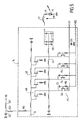
En référence à la figure 5, on a remplacé le circuit de filtrage d'alimentation PD en tension VD de la ligne de drains commune décrite en référence aux figures 2 et 3 par un circuit de filtrage de polarisation PS utilisant des transistors supplémentaires TS fonctionnant en charge saturable. Referring to Figure 5, we replaced the circuit power supply filtering PD in voltage VD of the line common drains described with reference to Figures 2 and 3 by a polarization filter circuit PS using transistors additional TS operating at saturable load.
En pratique, le circuit PS comprend une pluralité de transistors supplémentaires TS fonctionnant en charge saturable. Les sources SS des transistors supplémentaires TS sont distributivement connectées sur la ligne de drains commune LD.In practice, the PS circuit includes a plurality of transistors additional TS operating at saturable load. The SS sources of additional TS transistors are distributively connected to the common line of drains LD.
Les drains DS des transistors supplémentaires TS reçoivent en série la tension de polarisation VD.The DS drains of the additional TS transistors receive series the bias voltage VD.
Les grilles GS des transistors supplémentaires reçoivent en série une seconde tension de polarisation de grille VG2, le cas échéant respectivement à travers une résistance supplémentaire RS. En pratique,la tension VG2 est reliée à la masse en parallèle à travers une capacité dé découplage CSS. De plus, chaque grille supplémentaire est reliée à sa source respective à travers une capacité supplémentaire CS.The GS grids of the additional transistors receive in series a second VG2 gate bias voltage, the if necessary respectively through additional resistance RS. In practice, the voltage VG2 is connected to ground in parallel through a CSS decoupling capacity. Of plus, each additional grid is linked to its source respective through additional capacity CS.
Le circuit PS remédie aux inconvénients (déperdition d'énergie, encombrement) résultant du filtrage des circuits de polarisation à travers des résistances terminales RG comme celle décrite en référence à la figure 2.The PS circuit remedies the drawbacks (energy loss, congestion) resulting from the filtering of the polarization across RG terminal resistors like that described with reference to Figure 2.
De même, le circuit PS remédie aux inconvénients (dégradations
des performances, désadaptation d'impédance, résonance,
encombrement, soudures) résultant du filtrage des circuits de
polarisation à travers des éléments selfiques 15, ID1, ID2,
ID3 comme ceux décrits en référence aux figures 2 et/ou 3.Similarly, the PS circuit remedies the disadvantages (degradations
performance, impedance mismatch, resonance,
dimensions, welds) resulting from the filtering of the
polarization through
En référence à la figure 6A, on a représenté un mode de réalisation de la diode de décalage qui comprend une pluralité de transistors à effet de champ réalisés en technologie intégrée monolithique hyperfréquence.Referring to Figure 6A, there is shown a mode of realization of the shift diode which comprises a plurality field effect transistors produced in technology integrated monolithic microwave.
La diode de décalage DD comprend par exemple deux rangées RA1 et RA2 de n transistors. Chaque transistor forme une diode élémentaire DE en reliant son drain à sa source.The shift diode DD comprises for example two rows RA1 and RA2 of n transistors. Each transistor forms a diode elementary DE by connecting its drain to its source.
Chaque transistor comprend un doigt de grille DG, individualisé en DG11 à DG1n pour la première rangée RA1 et en DG21 à DG2n pour la seconde rangée RA2. Each transistor includes a DG gate finger, individualized in DG11 to DG1n for the first row RA1 and in DG21 to DG2n for the second row RA2.
Par exemple, le courant de chaque doigt de grille DG est inférieur à 1 milliampère (pour n = 148) et le courant de polarisation VD de la ligne de drain LD est de l'ordre de 150 à 300 milliampères.For example, the current of each DG grid finger is less than 1 milliampere (for n = 148) and the current of VD polarization of the drain line LD is of the order of 150 at 300 milliamps.
Chaque doigt de grille DG de la diode DD est réalisé selon un contact dit "Schottky" SK similaire aux grilles des transistors à effet de champ. En pratique, un contact "Schottky" SK est un contact métal/semi-conducteur qui résulte en une barrière de potentiel AC. Un tel contact "Schottky" présente un effet diode.Each gate finger DG of the diode DD is produced according to a contact called "Schottky" SK similar to the transistor grids field effect. In practice, a "Schottky" SK contact is a metal / semiconductor contact that results in a AC potential barrier. Such a "Schottky" contact presents a diode effect.
En revanche, les drains et les sources des transistors de la diode de décalage sont réalisés selon un contact dit "ohmique" OH qui est un contact métal/semi conducteur nécessitant une métallurgie plus complexe que celle du contact Schottky SK. Un tel contact ohmique implique généralement des matériaux du type Germanium, Or, ou Arséniure de Gallium, et résulte en l'absence de barrière de potentiel. C'est donc un contact sans effet diode avec une résistance de faible valeur.On the other hand, the drains and the sources of the transistors of the shift diode are made according to a so-called "ohmic" contact OH which is a metal / semiconductor contact requiring a more complex metallurgy than that of the Schottky contact SK. Such ohmic contact generally involves materials of the Germanium, Gold, or Gallium Arsenide type, and results in the absence of a potential barrier. So it's a contact without diode effect with low resistance value.
La zone intermédiaire AC entre le contact ohmique et le contact Schottky est une zone active.The intermediate zone AC between the ohmic contact and the Schottky contact is an active area.
Chaque doigt de grille a un développement individuel de l'ordre de 5 micromètres. Ainsi, la diode de décalage a un développement de grille total de l'ordre de 148 x 5 micromètres, soit de l'ordre de 740 micromètres.Each grid finger has an individual development of around 5 micrometers. So the shift diode has a total grid development of the order of 148 x 5 micrometers, or of the order of 740 micrometers.
En référence à la figure 7, on a représenté un masque qui
illustre la réalisation du circuit 16 décrit en référence à
la figure 3 et qui comprend un amplificateur distribué 18
selon l'invention et une diode de décalage DD.Referring to Figure 7, there is shown a mask which
illustrates the construction of
En référence à la figure 6B, on a représenté une portion agrandie du masque de la diode de décalage dans laquelle on distingue parfaitement les doigts de grille DG.Referring to Figure 6B, there is shown a portion enlarged mask of the shift diode in which we perfectly distinguishes the DG grid fingers.
Claims (11)
caractérisé en ce qu'il comprend une diode (DD) de décalage en tension réalisée en technologie intégrée monolithique hyperfréquence, montée entre la sortie (S) du circuit amont (16) et l'entrée du circuit aval (18), la caractéristique de la diode de décalage (DD) étant choisie de telle sorte que la tension de polarisation (VD) du circuit amont (16) soit décalée d'un décalage correspondant sensiblement à l'écart entre les tensions de polarisation (VD et VL) des circuits amont (16) et aval (8), et en ce que le courant de polarisation du circuit aval étant relativement élevé par rapport au courant de seuil de la diode de décalage.Interface device between two circuits, the upstream circuit of which comprises an output and DC voltage biasing means and the said downstream circuit of which includes an input, requires a DC bias voltage of higher value than that of the upstream circuit, and consumes a relatively large bias current which is a function of the power delivered by the downstream circuit,
characterized in that it comprises a voltage shift diode (DD) produced in integrated monolithic microwave technology, mounted between the output (S) of the upstream circuit (16) and the input of the downstream circuit (18), the characteristic of the offset diode (DD) being chosen so that the bias voltage (VD) of the upstream circuit (16) is offset by an offset corresponding substantially to the difference between the bias voltages (VD and VL) of the circuits upstream (16) and downstream (8), and in that the bias current of the downstream circuit is relatively high compared to the threshold current of the offset diode.
Applications Claiming Priority (2)
| Application Number | Priority Date | Filing Date | Title |
|---|---|---|---|
| FR0016937A FR2818829B1 (en) | 2000-12-22 | 2000-12-22 | VOLTAGE SHIFT DIODE MADE IN INTEGRATED MONOLITHIC MICROWAVE TECHNOLOGY, ESPECIALLY FOR A VERY WIDE BAND MICROPHONE OPTOELECTRONIC TRANSMITTER |
| FR0016937 | 2000-12-22 |
Publications (1)
| Publication Number | Publication Date |
|---|---|
| EP1217725A1 true EP1217725A1 (en) | 2002-06-26 |
Family
ID=8858122
Family Applications (1)
| Application Number | Title | Priority Date | Filing Date |
|---|---|---|---|
| EP01403225A Withdrawn EP1217725A1 (en) | 2000-12-22 | 2001-12-12 | Monolithic integrated microwave voltage level shifting diode especially for microwave broadband optoelectronic transmitter |
Country Status (4)
| Country | Link |
|---|---|
| US (1) | US20020139998A1 (en) |
| EP (1) | EP1217725A1 (en) |
| JP (1) | JP2002290169A (en) |
| FR (1) | FR2818829B1 (en) |
Cited By (1)
| Publication number | Priority date | Publication date | Assignee | Title |
|---|---|---|---|---|
| US6730945B2 (en) * | 2001-09-26 | 2004-05-04 | Mitsubishi Denki Kabushiki Kaisha | Semiconductor device |
Families Citing this family (3)
| Publication number | Priority date | Publication date | Assignee | Title |
|---|---|---|---|---|
| US6924697B2 (en) * | 2003-02-27 | 2005-08-02 | Freescale Semiconductor, Inc. | Semiconductor device and method thereof |
| JP2014096405A (en) * | 2012-11-07 | 2014-05-22 | Sumitomo Electric Ind Ltd | Optical transmission circuit |
| CN104883800B (en) * | 2015-06-15 | 2017-04-12 | 南京大学 | GHz high-speed LED optical communication driver |
Citations (2)
| Publication number | Priority date | Publication date | Assignee | Title |
|---|---|---|---|---|
| EP0801467A1 (en) * | 1996-04-11 | 1997-10-15 | Dassault Electronique | Low impedance distributed amplifier adapter for opto-electronic microwave signal transmitter with very wide band |
| US5880640A (en) * | 1989-11-24 | 1999-03-09 | Dassault Electronique | Distributed amplifier for wide band hyperfrequency signals |
Family Cites Families (2)
| Publication number | Priority date | Publication date | Assignee | Title |
|---|---|---|---|---|
| FR2661790B1 (en) * | 1990-05-03 | 1995-08-25 | France Etat | VERY BROADBAND CONTINUOUS-MICROWAVE AMPLIFICATION DEVICE, ESPECIALLY REALIZABLE IN INTEGRATED CIRCUIT. |
| GB9920081D0 (en) * | 1999-08-24 | 1999-10-27 | Sgs Thomson Microelectronics | Current reference circuit |
-
2000
- 2000-12-22 FR FR0016937A patent/FR2818829B1/en not_active Expired - Fee Related
-
2001
- 2001-12-05 US US10/001,978 patent/US20020139998A1/en not_active Abandoned
- 2001-12-06 JP JP2001372331A patent/JP2002290169A/en not_active Withdrawn
- 2001-12-12 EP EP01403225A patent/EP1217725A1/en not_active Withdrawn
Patent Citations (3)
| Publication number | Priority date | Publication date | Assignee | Title |
|---|---|---|---|---|
| US5880640A (en) * | 1989-11-24 | 1999-03-09 | Dassault Electronique | Distributed amplifier for wide band hyperfrequency signals |
| EP0801467A1 (en) * | 1996-04-11 | 1997-10-15 | Dassault Electronique | Low impedance distributed amplifier adapter for opto-electronic microwave signal transmitter with very wide band |
| FR2747523A1 (en) * | 1996-04-11 | 1997-10-17 | Dassault Electronique | AMPLIFIER DISPENSES LOW IMPEDANCE LOW ADAPTER FOR OPTOELECTRONIC TRANSMITTER OF VERY BROADBAND MICROWAVE SIGNALS |
Non-Patent Citations (1)
| Title |
|---|
| KIMURA S ET AL: "A 0-TO-40-GHZ DIRECT-COUPLED DISTRIBUTED BASEBAND AMPLIFIER IC WITHSCFL INTERFACE", IEEE MICROWAVE AND GUIDED WAVE LETTERS, IEEE INC, NEW YORK, US, vol. 6, no. 12, 1 December 1996 (1996-12-01), pages 444 - 446, XP000635323, ISSN: 1051-8207 * |
Cited By (1)
| Publication number | Priority date | Publication date | Assignee | Title |
|---|---|---|---|---|
| US6730945B2 (en) * | 2001-09-26 | 2004-05-04 | Mitsubishi Denki Kabushiki Kaisha | Semiconductor device |
Also Published As
| Publication number | Publication date |
|---|---|
| US20020139998A1 (en) | 2002-10-03 |
| FR2818829A1 (en) | 2002-06-28 |
| JP2002290169A (en) | 2002-10-04 |
| FR2818829B1 (en) | 2003-03-28 |
Similar Documents
| Publication | Publication Date | Title |
|---|---|---|
| EP0675422B1 (en) | Regulator circuit generating a reference voltage independent of temperature or supply voltage | |
| EP3866337A1 (en) | Class ad audio amplifier | |
| EP0455570B1 (en) | Very wide bandwidth amplifier device for DC to microwave frequencies, particularly in the form of an integrated circuit | |
| EP0586285B1 (en) | Emitting-receiving optical head for optical data transmission and switching circuit for the head | |
| EP1217725A1 (en) | Monolithic integrated microwave voltage level shifting diode especially for microwave broadband optoelectronic transmitter | |
| FR2842963A1 (en) | ACTIVE CHARGING DEVICE FOR POLARIZING A BROADBAND DISTRIBUTED AMPLIFIER CIRCUIT WITH GAIN CONTROL | |
| EP2788782B1 (en) | Device for detecting pulsed electromagnetic radiation | |
| EP0318379A1 (en) | Ultra-high frequency amplifier with a very wide pass band | |
| EP0726648B1 (en) | Tuning circuit for a receiver apparatus particularly a television receiver | |
| FR2638287A1 (en) | ACOUSTIC SURFACE WAVE DEVICE | |
| EP0199332A1 (en) | Wide-band receiver for optical signals | |
| EP0368742B1 (en) | Digital amplifier and integrated circuit including such | |
| EP0120756B1 (en) | Oscillator comprising high-frequency bandpass amplifier having an adaptable impedance | |
| EP0420106B1 (en) | Attenuator using a dual gate field effect transistor | |
| EP1017171B1 (en) | Phase control device with a plurality of distributed amplifier structures with switchable active elements for constituting a programmable length line | |
| EP0801467B1 (en) | Low impedance distributed amplifier adapter for opto-electronic microwave signal transmitter with very wide band | |
| FR2826802A1 (en) | BROADBAND POLARIZATION DEVICE OF AN ELECTRONIC CIRCUIT AND AMPLIFIER INCORPORATING THE SAME | |
| FR2759508A1 (en) | Distributed amplifier for telecommunications | |
| EP0986170A1 (en) | Interfacing device between a broadband microwave opto-electronic sensor and a load | |
| EP3235125A1 (en) | Improved amplifier channel such as a gain block device | |
| FR2747524A1 (en) | HIGH IMPEDANCE ADAPTER AMPLIFIER FOR RECEIVING VERY BROADBAND MICROWAVE SIGNALS FROM A HIGH IMPEDANCE CAPACITIVE SOURCE SUCH AS A PHOTODIODE | |
| JP2923969B2 (en) | Light switch | |
| FR2955721A1 (en) | Adjustable gain wideband distributed microwave amplifier cell for monolithic microwave integrated circuit of electronic system, has two transistors assembled in cascode manner, where gain of amplifier cell is adjusted | |
| FR2955722A1 (en) | Adjustable gain dual output microwave amplifier cell for adjustable gain splitter of monolithic microwave integrated circuit in electronic system, has lines whose gains are adjusted by controlling differential voltage between gates | |
| JP2018060976A (en) | Direct modulation laser |
Legal Events
| Date | Code | Title | Description |
|---|---|---|---|
| PUAI | Public reference made under article 153(3) epc to a published international application that has entered the european phase |
Free format text: ORIGINAL CODE: 0009012 |
|
| AK | Designated contracting states |
Kind code of ref document: A1 Designated state(s): AT BE CH CY DE DK ES FI FR GB GR IE IT LI LU MC NL PT SE TR |
|
| AX | Request for extension of the european patent |
Free format text: AL;LT;LV;MK;RO;SI |
|
| 17P | Request for examination filed |
Effective date: 20020607 |
|
| D17P | Request for examination filed (deleted) | ||
| R17P | Request for examination filed (corrected) |
Effective date: 20021209 |
|
| AKX | Designation fees paid |
Designated state(s): AT BE CH CY DE DK ES FI FR GB GR IE IT LI LU MC NL PT SE TR |
|
| STAA | Information on the status of an ep patent application or granted ep patent |
Free format text: STATUS: THE APPLICATION IS DEEMED TO BE WITHDRAWN |
|
| 18D | Application deemed to be withdrawn |
Effective date: 20050701 |