EP0368742B1 - Digital amplifier and integrated circuit including such - Google Patents
Digital amplifier and integrated circuit including such Download PDFInfo
- Publication number
- EP0368742B1 EP0368742B1 EP89403053A EP89403053A EP0368742B1 EP 0368742 B1 EP0368742 B1 EP 0368742B1 EP 89403053 A EP89403053 A EP 89403053A EP 89403053 A EP89403053 A EP 89403053A EP 0368742 B1 EP0368742 B1 EP 0368742B1
- Authority
- EP
- European Patent Office
- Prior art keywords
- transistor
- amplifier
- output
- transistors
- low
- Prior art date
- Legal status (The legal status is an assumption and is not a legal conclusion. Google has not performed a legal analysis and makes no representation as to the accuracy of the status listed.)
- Expired - Lifetime
Links
- 238000010200 validation analysis Methods 0.000 claims description 24
- 230000005669 field effect Effects 0.000 claims description 22
- 230000000295 complement effect Effects 0.000 claims description 11
- 229910052745 lead Inorganic materials 0.000 claims description 7
- 238000007599 discharging Methods 0.000 claims description 2
- 230000003321 amplification Effects 0.000 description 9
- 238000003199 nucleic acid amplification method Methods 0.000 description 9
- 238000005516 engineering process Methods 0.000 description 7
- 238000010586 diagram Methods 0.000 description 4
- 230000005540 biological transmission Effects 0.000 description 3
- 230000000694 effects Effects 0.000 description 3
- 230000036039 immunity Effects 0.000 description 3
- 239000000243 solution Substances 0.000 description 3
- 230000010287 polarization Effects 0.000 description 2
- 239000004065 semiconductor Substances 0.000 description 2
- 230000000903 blocking effect Effects 0.000 description 1
- 238000004891 communication Methods 0.000 description 1
- 230000000593 degrading effect Effects 0.000 description 1
- 230000008030 elimination Effects 0.000 description 1
- 238000003379 elimination reaction Methods 0.000 description 1
- 230000006870 function Effects 0.000 description 1
- 230000010365 information processing Effects 0.000 description 1
- 238000002347 injection Methods 0.000 description 1
- 239000007924 injection Substances 0.000 description 1
- 238000002955 isolation Methods 0.000 description 1
- 239000000463 material Substances 0.000 description 1
- 229910044991 metal oxide Inorganic materials 0.000 description 1
- 150000004706 metal oxides Chemical class 0.000 description 1
- 239000000203 mixture Substances 0.000 description 1
Images

Classifications
-
- H—ELECTRICITY
- H03—ELECTRONIC CIRCUITRY
- H03K—PULSE TECHNIQUE
- H03K19/00—Logic circuits, i.e. having at least two inputs acting on one output; Inverting circuits
- H03K19/02—Logic circuits, i.e. having at least two inputs acting on one output; Inverting circuits using specified components
- H03K19/08—Logic circuits, i.e. having at least two inputs acting on one output; Inverting circuits using specified components using semiconductor devices
- H03K19/094—Logic circuits, i.e. having at least two inputs acting on one output; Inverting circuits using specified components using semiconductor devices using field-effect transistors
- H03K19/0944—Logic circuits, i.e. having at least two inputs acting on one output; Inverting circuits using specified components using semiconductor devices using field-effect transistors using MOSFET or insulated gate field-effect transistors, i.e. IGFET
- H03K19/09448—Logic circuits, i.e. having at least two inputs acting on one output; Inverting circuits using specified components using semiconductor devices using field-effect transistors using MOSFET or insulated gate field-effect transistors, i.e. IGFET in combination with bipolar transistors [BIMOS]
-
- H—ELECTRICITY
- H03—ELECTRONIC CIRCUITRY
- H03K—PULSE TECHNIQUE
- H03K19/00—Logic circuits, i.e. having at least two inputs acting on one output; Inverting circuits
- H03K19/01—Modifications for accelerating switching
- H03K19/013—Modifications for accelerating switching in bipolar transistor circuits
- H03K19/0136—Modifications for accelerating switching in bipolar transistor circuits by means of a pull-up or down element
Definitions
- the invention relates to binary amplifiers and circuits integrated incorporating them. More specifically, it concerns binary amplifiers integrated in a semiconductor material and essentially composed of at least one associated field effect transistor to bipolar transistors. It is more particularly adapted to integrated circuits including type field effect transistors complementary and bipolar transistors, such as circuits BiCMOS integrated in which the field effect transistors are of the type CMOS (Complementary Metal Oxide Semiconductor).
- the invention applies especially to binary transmission amplifiers in communication systems information processing, such as interface amplifiers (buffer amplifiers) connected to the output terminals of a circuit integrated to transmit a binary signal to a load circuit.
- the charging circuit can be a bus, or a link with a integrated memory.
- a third state logic called high impedance, controlled by a validation signal.
- the binary amplifier provides electrical isolation with the bus so as not to interfere with the signals transmitted on the bus from from another amplifier.
- the invention also relates to these amplifiers.
- Integrated binary amplifiers composed of a transistor effect field as an input element and of a bipolar transistor as an element of have the disadvantage of degrading operation when the capacity of its charging circuit exceeds a relatively low value, 10 pF for example.
- One solution is to associate with the effect transistor of field two bipolar transistors in cascade (Darlington assembly). For optimize the signal propagation time in the amplifier, we eliminates the electrical charges that have accumulated on the bases of bipolar transistors. Elimination takes place during the blocking period bipolar transistors, by means of discharge elements connecting the respective bases of the transistors at a supply potential, the mass usually. Each discharge element is the resistance serving as polarization of the bipolar transistors during their operation, or a field effect transistor in an amplifier not using resistance.
- Such an amplifier has the advantage of tolerating strong capacities of its charging circuit, up to 200 pF for example, and require the use of normal size transistors.
- the same advantages are obtained by applying the same solution to conventional binary amplifiers composed of at least two field effect transistors associated respectively with a transistor bipolar.
- the simplest of these amplifiers includes two transistors field effect of complementary types receiving the same input signal.
- the field effect transistor for amplifying the high level is associated with two bipolar cascade transistors.
- the effect transistor field for amplification of the low level is associated with a single transistor bipolar.
- the base of each bipolar transistor is provided with a capacity discharge element, which can be a resistance or a field effect transistor.
- a capacity discharge element which can be a resistance or a field effect transistor.
- the cascading of bipolar transistors has the disadvantage of reduce the excursion of the output signal.
- This drawback appears clearly by using for example an amplifier composed of a couple of CMOS transistors each associated with two bipolar cascade transistors.
- Vbe base-emitter junction voltage
- the output signal oscillates between approximately 1.6 volts and 3.4 volts.
- the amplitude of the output signal is only about 2.6 volts, i.e. approximately half of the supply voltage (5 volts).
- the first consequence of such a weakened amplitude is that the signal output is very sensitive to noise.
- a spurious signal can alter the operation of the component controlled by the amplifier.
- the output signal can no longer be compatible with a load circuit including an integrated circuit - a memory integrated by example - made in TTL technology (Transistor-Transistor Logic).
- TTL technology Transistor-Transistor Logic
- This technology requires potentials that cannot be reached by a output signal from the binary amplifier too weak.
- the third consequence is the need to have a supply voltage high. This requirement contrasts with the current trend to use more low supply voltages, 3 volts for example.
- the voltage Vbe is generative, in numerous applications, of a stray current in the charging circuit of the amplifier. For example, if the charging circuit is a memory integrated, composed of numerous cells, a leakage current flows through transfer transistors of each cell, so that the set of leakage currents in cells produce potential differences relatively high that can disrupt the desired operation of the memory.
- the amplification of the low level is usually done by a single bipolar transistor while the amplification of the high level is made by a Darlington assembly, as illustrated in the aforementioned US Pat. No. 4,638,186. This therefore significantly limits the desired performance of the amplifier.
- the amplifier output circuit also includes a bipolar transistor for amplification of the low level, and two cascaded transistors constituting a Darlington circuit for amplification of the high level.
- the low level bipolar transistor is of the Schottky type in order to present a voltage Vbe of approximately 0.3 volts.
- the voltage Vbe of the first transistor is substantially shunted by a link applying the base of the output bipolar transistor to the high supply potential.
- the operating principle of the shunt link which is described and illustrated in this patent does not answer the problem posed by the amplification of the low level and presented above.
- the invention provides a simple and effective solution to respond to the problem posed by the amplification of the low level while retaining the advantages of cascaded transistors in a BiMOS or BiCMOS amplifier in view obtain a large excursion output signal, substantially equal to the supply voltage.
- the invention thus provides immunity to noise and compatibility with TTL technology, and allows the application of a low supply voltage and extension of the number of transistors bipolar cascade for amplification of high and low levels.
- a first version referring to Figures 1 to 3 and a second version referring to Figures 4 and 5 of a integrated binary amplifier according to the invention are respectively defined by claims 1 and 3.
- an integrated circuit according to the invention is characterized in what it includes at least one amplifier as defined above.
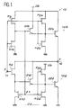
- the illustrated examples of amplifiers 10 according to the invention relate to the biCMOS technology.
- the amplifiers 10 are supplied with electrical energy under two potentials Ua (ground) and Ub (+ 5 volts), for example. They receive the input signal e and deliver the output signal s .
- the n-MOS transistors are designated by N, the p-MOS transistors by P, and the bipolar transistors by Q.
- Figures 1 and 2 respectively represent the two families of the same type of amplifier 10 according to the invention.
- the amplifiers 10 receive the input signal e on an input terminal 11 and deliver an output signal s on an output terminal 12.
- the amplifiers 10 of FIGS. 1 and 2 have two stable states and constitute inverters formed on the basis of a pair of CMOS, Na and Pb transistors.
- Two amplifiers 10a, 10b are defined in the amplifiers 10 respectively linked to the CMOS, Na and Pb transistors.
- the transistors Na and Pb are respectively in series with the first transistors N1a and N1b having their source at ground.
- the transistors Na and N1a have their drain-source paths in series, like the transistors Pb and N1b.
- the drain of the transistor Na is connected to the output terminal 12 and the drain of the transistor Pb is connected to the supply potential Ub.
- the gates of the transistors Na, Pb and N1b are connected to the input terminal 11 to receive the input signal e .
- the gate of transistor N1a is connected to the source of transistor Pb representative of the complementary input signal e *.
- the potential Ub is applied to the collectors of a group of two bipolar transistors Q1b and Q2b connected in cascade.
- the transistor Q1b has its base connected to the source of the transistor Pb and its emitter connected to the base of the transistor Q2b.
- the output terminal 12 is connected to the emitter of the transistor Q2b as well as to the collectors of another group of two bipolar transistors Q1a and Q2a connected in cascade.
- the transistor Q1a has its base connected to the source of the transistor Na and its emitter connected to the base of the transistor Q2a having its emitter to ground.
- the transistors Q1a, Q2a form a Darlington circuit, like the transistors Q1b and Q2b.
- the bases of the transistors Q2a and Q2b are respectively connected to the drains of two second transistors N2a, N2b having their sources at ground.
- the gate of transistor N2b receives the input signal e and the gate of transistor N2a receives the complementary input signal e * .
- the transistor Na is blocked and the transistor Pb conducts.
- the transistors Q1a and Q2a are blocked, while the transistors Q1b and Q2b conduct.
- the transistors N1a and N2a conduct and discharge the bases of the transistors Q1a and Q2a, while the transistors N1b and N2b are blocked.
- the output signal s on terminal 12 therefore has logic level "1".
- the transistors Pb, Q1b, Q2b are no longer conductive.
- the transistors N1b and N2b conduct and thus flow to ground the charges which had accumulated on the bases of the respective bipolar transistors Q1b and Q2b during their operation.
- the transistors Na, Q1a, Q2a become conductive and the transistors N1a and N2a become non-conductive.
- the output signal s therefore takes logic level "0".
- a first advantage of the amplifier 10 as illustrated is to be able function properly despite a very high capacity (up to 200 pF for example) of the load circuit connected to the output terminal 12.
- the second advantage lies in the dimensions of the transistors amplifier 10, which need not be increased to provide the first advantage.
- the low and high levels of the output signal corresponding to the logical states "0" and "1" deviate respectively from potentials Ua and Ub of the value 2Vbe, where Vbe denotes the voltage of base-emitter junction of a bipolar transistor which can reach 0.8 volt.
- the invention consists in connecting in each section 10a, 10b the base of each bipolar output transistor Q2a, Q2b to the supply potential Ub via the drain-source path of a third field effect transistor whose type and the control ensure its conduction when the bipolar transistors of the group associated with the output transistor are conductive.
- a third field effect transistor whose type and the control ensure its conduction when the bipolar transistors of the group associated with the output transistor are conductive.
- the output signal s of the amplifier 10 has a low level substantially equal to Ua (0 volts) and a high level which differs from the potential Ub by a single Vbe, ie at most 0 , 8 volts.
- the output signal s retains good noise immunity and can be adapted to TTL technology.
- the amplifier 10 retains its advantages if one or more cascade transistors are added in each section 10a, 10b.
- Amplifier 10 can therefore adapt to very high load capacities, greater than 200 pF for example, by associating each transistor Na, Pb with at least three bipolar transistors in cascade.
- the addition of the transistors P3a and P3b to the respective bipolar output transistors Q2a, Q2b will also provide an output signal s similar to that supplied by the amplifier 10 shown in FIG. 1.
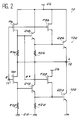
- the amplifier 10 of FIG. 2 is an alternative embodiment of the amplifier 10 shown in FIG. 1.
- the transistors N1a, N2a, N1b, N2b of FIG. 1 are replaced by resistors R1a, R2a, R1b, R2b.
- the resistors R1a and R1b are in series with the transistors Na and Pb.
- the resistors R1a and R2a connect the bases of the transistors Q1a, Q2a respectively to the potential Ua.
- the resistors R1b, R2b respectively connect the bases of the transistors Q1b, Q2b to the drain of the transistor Na and to the terminal 12.
- each bipolar output transistor Q2a, Q2b is connected to the potential Ub by means of a field effect transistor P3a, P3b.
- the transistor P3a has its gate connected to the source of the transistor Pb to receive the complementary input signal e * .
- the transistor P3b has its gate connected to the input terminal 11 to receive the input signal e .
- the conduction of transistor P3a maintains the low level of the output signal s at a value very close to ground.
- the conduction of transistor P3b brings the high level of the output signal s to Ub - Vbe.
- a third cascaded bipolar transistor could be included in each section 10a, 10b and obtain the same advantages.
- the amplifier 10 shown in FIG. 3 constitutes a second type of amplifiers in accordance with the invention, intended to deliver their output signal to a bus and called bus transmitters.
- the amplifier 10 of the second type has three logic states and has a structure based on the first type of amplifier as shown in FIG. 1. In FIGS. 1 and 3, the same elements bear the same reference numbers.
- the amplifier 10 carries a second input terminal 13 for a validation signal v , which is added to the input signal e applied to the input terminal 11.
- the second type of amplifier 10 is above all a buffer amplifier, the output terminal 12 of which corresponds in the example illustrated to the output terminal of an integrated circuit IC partially and schematically delimited by a phantom line in FIG. 3.
- the output terminal 12 can be connected to a separate output terminal of the integrated circuit.
- the output terminal 12 is intended for a connection with a bus 14 external to the integrated circuit IC, as illustrated.
- the two sections 10a, 10b of the amplifier 10 are also formed by the two CMOS transistors Na and Pb receiving on their gates the input signal e . They are associated in the same way with the transistors N1a and N1b, as well as with the bipolar transistors Q1a, Q2a; Q1b, Q2b.
- the transistors N1a, N2a, N1b, N2b are connected in the same way as in FIG.
- the transistor Na has its drain connected to the output terminal 12 via a transitor Pa receiving the validation signal v on its gate.
- the transistor Pb has its drain connected to the potential Ub via a transistor P'b receiving the validation signal v on its gate.
- the bases of the bipolar output transistors Q2a, Q2b are respectively connected to the potential Ub via the transistors P3a, P3b, whose gates are connected in the same way as in FIG. 1 and whose paths drain-source are in series with those of two respective additional transistors P'3a, P'3b receiving the validation signal v on their gate.
- the transistors Pa and P'b are non-conductive.
- the amplifier 10 is thus placed in the non-operating state and has a high impedance to any external signal applied to the output terminal 12. In this state, the amplifier 10 does not disturb the transmission of any signal on the bus 14 emanating another amplifier 10 associated with the bus.
- the validation signal v has the logic state "0" it authorizes the normal operation of all the transistors of the amplifier 10 which are common with those of FIG. 1, so as to give an output signal s complementary to the input signal e .
- the transistors P'3a, P'3b are then in on-condition to allow the normal operation of the transistors P3a and P3b according to the invention.
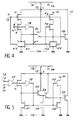
- FIGS. 4 and 5 illustrate amplifiers 10 of a third type to which the invention can also be applied. These amplifiers are suitable for connection to a preloaded bus 15 and commonly known as preloaded bus transmitters.
- the presence of the bus 15 implies that they have three states, like the amplifier 10 represented in FIG. 3.
- the amplifiers 10 of FIGS. 4 and 5 receive an input signal e and a validation signal v , and their output terminal 12 is connected to bus 15.
- bus 15 in FIGS. 4 and 5 is preloaded, usually at the high level corresponding to the potential Ub. In this way, the amplifiers 10 of FIGS. 4 and 5 conventionally receive only the potential Ua (ground).
- the circuit of the amplifier 10 represented in FIG. 4 corresponds to section 10a of the amplifier 10 represented in FIG. 3.
- the output terminal 12 is connected to ground via the transistors P, N and N1 connected in series.
- the input signal e on the input terminal 11 is applied to the gate of the transistor N as well as to the input of an inverter 16, which supplies the complementary input signal e * to the transistor N1.
- the validation signal v on the validation terminal 13 is applied to the gate of the transistor P.
- the junction of the source of the transistor N with the drain of the transistor N1 is connected to the bipolar transistor Q1, whose collector is connected to the terminal of output 12 and whose emitter is connected to the base of the bipolar output transistor Q2.
- the transistor Q2 has its emitter to ground and its collector connected to the output terminal 12. Its base is connected to ground by the transistor N2 and to a fixed potential Uc (+ 3 volts, for example) via the two transistors P3 and P'3 connected in series.
- the transistors N1 and N2 are connected in parallel with respective transistors N'1 and N'2.
- the gates of the transistors N1, N2 and P3 receive the complementary input signal e *.
- the gates of the transistors P, N'1, N'2 and P'3 receive the validation signal v .
- the transistors P and P'3 are blocked, while the transistors N'1 and N'2 are conductive, thus discharging the capacities of the bases of the transistors Q1 and Q2 .
- the amplifier 10 thus has at its output terminal 12 a high impedance for the transmission of any signal on the bus 15 emitted by another amplifier associated with the bus. If the amplifier 10 shown in FIG. 4 is to transmit, the validation signal v takes the logic state "0". Under these conditions, the transistors P and P'3 are conductive and the transistors N'1 and N'2 are blocked, so that the transistors N, Q1, Q2, N1, N2 and P3 can operate normally so that the bus takes the logic state of the input signal e .
- the transistors N, P3, Q1, Q2 are conductive and the transistors N1 and N2 are blocked.
- the transistors N and P thus authorize the injection of a current into the base of the transistor Q1.
- the transistors Q1 and Q2 amplify this current and allow the rapid discharge of the capacity formed by the bus 15. Without the transistors P3 and P'3 added in accordance with the invention, the low levels of the bus 15 corresponding to the input signal e in the logic state "1" would have the value of the 2Vbe of the transistors Q1 and Q2, ie a value less than or equal to 1.6 volts.
- the low level of the bus 15 can reach the value of the potential Ua, the mass in this case.
- the transistors P3 and P'3 conduct to inject a current into the base of the bipolar transistor Q2 during the discharge of the bus 15.
- the injected current is of the order of a few tens of micro-amps, so that the resulting dissipation is very low.
- the signal transmitted on the bus offers great immunity to noise and can be adapted to TTL technology. In addition, it has these same advantages regardless of the number of bipolar transistors of the group associated with transistor N receiving the input signal e .
- FIG. 5 shows an amplifier 10 according to the invention, constituting an alternative embodiment of the amplifier 10 shown in Figure 4.
- the same components are designated by the same reference numerals.
- This variant gives the amplifier 10 of FIG. 5 a structure partially identical to that of section 10a of the amplifier 10 shown in FIG. 1.
- the output terminal 12 connected to the preloaded bus 15 is connected to the supply potential Ua (the mass) by the transistors N and N1 and, on the other hand, by a group formed by the two bipolar transistors Q1 and Q2 and by an additional bipolar transistor Q3, all connected in cascade according to a Darlington configuration.
- the junction of the source of transistor N with the drain of transistor N1 is connected to the base of transistor Q1.
- the emitter of transistor Q1 is connected to the base of the additional transistor Q3.
- the output transistor Q2 has its emitter to ground, its base connected to the emitter of the transistor Q3 and its collector joined to the collectors of the transistors Q1 and Q3 as well as to the output terminal 12.
- the base of the output transistor Q2 is connected to ground by the transistor N2 and to a fixed potential Uc (+ 3 volts for example) by a transistor P3.
- the base of transistor Q3 is also discharged to ground under the action of a field effect transistor N3.
- the input signal e on the input terminal 11 and the validation signal v on the validation terminal 13 are applied to a NOR gate 17, the output of which is applied directly to the gate of the transistor N and, by the intermediate of the inverter 16, on the gates of the transistors N1, N2, N3 and P3.
- the inverter 16 and the NOR gate 17 are advantageously made in CMOS technology.
- the amplifier 10 of FIG. 5 is not selected to transmit on the bus 15.
- the transistor N is blocked and the transistor N1 conducts so that the base of transistor Q1 is grounded.
- the transistors Q1, Q2 and Q3 are therefore blocked and their bases discharged by the respective transistors N1, N2 and N3.
- the equivalent capacity formed by the bus 15 remains preloaded at the high level corresponding to the potential Ub.
- the amplifier 10 is to transmit on the bus 15, the validation signal v takes the logic state "0". If the input signal is logic state "1", the amplifier remains in the previous state. On the other hand, if the input signal e has the logic state "0", the transistors N and P3 conduct while the transistors N1 and N2 are blocked.
- the transistors Q1, Q3 and Q2 conduct to discharge the capacitance formed by the bus 15. Thanks to the transistor P3, the bus discharges to reach the value of the potential Ua, ie 0 volts.
- FIG. 5 which illustrates a group of three bipolar cascaded transistors can be applied to other amplifiers 10 illustrated.
- the variant of the figure 5 is inspired by section 10a of the amplifier 10 shown in the Figure 1, it can also undergo the variant of section 10a of the amplifier 10 shown in FIG. 2.
- the transistors N1, N2 and N3 in Figure 5 could be replaced by resistors R1, R2 and R3.
- a mix of resistors and transistors as basic discharge elements could be done in the same group of cascaded transistors.
- the above description highlights the application of the invention for any binary amplifier incorporating at least one field effect transistor reacting to an input signal and associated with at least two bipolar transistors in cascade .
- the invention then consists in connecting the base of the output bipolar transistor to a fixed potential via a field effect transistor whose type and control ensure its conduction when the bipolar transistors are conductive. It is clear that the presence of a discharge element from the base of each bipolar transistor is not necessary to obtain the advantages of the invention. The discharge elements only serve to increase the transit time of the input signal e in the amplifier 10 to the output terminal 12. In this sense, they will in practice always be advantageously associated with the bipolar transistors.
- the preceding description has also highlighted the fact that the control of a transistor by the input signal e or the validation signal v includes their complements e * and v *.
Description
L'invention se rapporte aux amplificateurs binaires et aux circuits intégrés les incorporant. Plus précisément, elle concerne les amplificateurs binaires intégrés dans un matériau semiconducteur et essentiellement composés d'au moins un transistor à effet de champ associé à des transistors bipolaires. Elle est plus particulièrement adaptée aux circuits intégrés incluant des transistors à effet de champ de types complémentaires et des transistors bipolaires, tels s que les circuits intégrés BiCMOS dans lesquels les transistors à effet de champ sont du type CMOS (Complementary Metal Oxide Semiconductor). L'invention s'applique notamment aux amplificateurs binaires de transmission dans des systèmes de traitement de l'information, tels que les amplificateurs d'interface (amplificateurs tampons) connectés aux bornes de sortie d'un circuit intégré pour transmettre un signal binaire à un circuit de charge. Par exemple, le circuit de charge peut être un bus, ou une liaison avec une mémoire intégrée. Dans les applications où plusieurs amplificateurs binaires sont reliés à un bus, on adjoint à chacun d'eux un troisième état logique, dit à haute impédance, commandé par un signal de validation. Dans cet état, l'amplificateur binaire assure une isolation électrique avec le bus de façon à ne pas interférer avec les signaux émis sur le bus à partir d'un autre amplificateur. L'invention concerne aussi ces amplificateurs.The invention relates to binary amplifiers and circuits integrated incorporating them. More specifically, it concerns binary amplifiers integrated in a semiconductor material and essentially composed of at least one associated field effect transistor to bipolar transistors. It is more particularly adapted to integrated circuits including type field effect transistors complementary and bipolar transistors, such as circuits BiCMOS integrated in which the field effect transistors are of the type CMOS (Complementary Metal Oxide Semiconductor). The invention applies especially to binary transmission amplifiers in communication systems information processing, such as interface amplifiers (buffer amplifiers) connected to the output terminals of a circuit integrated to transmit a binary signal to a load circuit. By example, the charging circuit can be a bus, or a link with a integrated memory. In applications where multiple amplifiers binaries are connected to a bus, we add to each of them a third state logic, called high impedance, controlled by a validation signal. In In this state, the binary amplifier provides electrical isolation with the bus so as not to interfere with the signals transmitted on the bus from from another amplifier. The invention also relates to these amplifiers.
Les amplificateurs binaires intégrés, composés d'un transistor à effet de champ comme élément d'entrée et d'un transistor bipolaire comme élément de sortie ont l'inconvénient d'avoir un fonctionnement se dégradant lorsque la capacité de son circuit de charge dépasse une valeur relativement faible, 10 pF par exemple. Une solution consiste à as'socier au transistor à effet de champ deux transistors bipolaires en cascade (montage Darlington). Pour optimiser le temps de propagation du signal dans l'amplificateur, on élimine les charges électriques qui se sont accumulées sur les bases des transistors bipolaires. L'élimination se fait pendant la période de blocage des transistors bipolaires, au moyen d'éléments de décharge reliant les bases respectives des transistors à un potentiel d'alimentation, la masse ordinairement. Chaque élément de décharge est la résistance servant de polarisation des transistors bipolaires pendant leur fonctionnement, ou un transistor à effet de champ dans un amplificateur n'utilisant pas de résistance. Un tel amplificateur a l'avantage de tolérer de fortes capacités de son circuit de charge, jusqu'à 200 pF par exemple, et de ne nécessiter l'emploi que de transistors de dimensions normales.Integrated binary amplifiers, composed of a transistor effect field as an input element and of a bipolar transistor as an element of have the disadvantage of degrading operation when the capacity of its charging circuit exceeds a relatively low value, 10 pF for example. One solution is to associate with the effect transistor of field two bipolar transistors in cascade (Darlington assembly). For optimize the signal propagation time in the amplifier, we eliminates the electrical charges that have accumulated on the bases of bipolar transistors. Elimination takes place during the blocking period bipolar transistors, by means of discharge elements connecting the respective bases of the transistors at a supply potential, the mass usually. Each discharge element is the resistance serving as polarization of the bipolar transistors during their operation, or a field effect transistor in an amplifier not using resistance. Such an amplifier has the advantage of tolerating strong capacities of its charging circuit, up to 200 pF for example, and require the use of normal size transistors.
Plus généralement, on obtient les mêmes avantages en appliquant la même solution aux amplificateurs binaires classiques composés d'au moins deux transistors à effet de champ associés respectivement à un transistor bipolaire. Le plus simple de ces amplificateurs inclut deux transistors à effet de champ de types complémentaires recevant le même signal d'entrée. Le transistor à effet de champ pour l'amplification du niveau haut est associé à deux transistors bipolaires en cascade. Le transistor à effet de champ pour l'amplification du niveau bas est associé à un seul transistor bipolaire. Dans l'amplificateur, la base de chaque transistor bipolaire est pourvue d'un élément de décharge de capacité, pouvant être une résistance ou un transistor à effet de champ. Un tel amplificateur est décrit dans le brevet US 4 638 186.More generally, the same advantages are obtained by applying the same solution to conventional binary amplifiers composed of at least two field effect transistors associated respectively with a transistor bipolar. The simplest of these amplifiers includes two transistors field effect of complementary types receiving the same input signal. The field effect transistor for amplifying the high level is associated with two bipolar cascade transistors. The effect transistor field for amplification of the low level is associated with a single transistor bipolar. In the amplifier, the base of each bipolar transistor is provided with a capacity discharge element, which can be a resistance or a field effect transistor. Such an amplifier is described in the U.S. Patent 4,638,186.
La mise en cascade de transistors bipolaires a cependant l'inconvénient de réduire l'excursion du signal de sortie. Cet inconvénient apparaít nettement en utilisant par exemple un amplificateur composé d'un couple de transistors CMOS associés chacun à deux transistors bipolaires en cascade. On sait que la tension de jonction base-émetteur (Vbe) d'un transistor bipolaire peut atteindre 0,8 volt. Par conséquent, si par exemple les potentiels d'alimentation sont la masse et + 5 volts, le signal de sortie oscille entre environ 1,6 volts et 3,4 volts. En d'autres termes, l'amplitude du signal de sortie est seulement de 2,6 volts environ, soit approximativement la moitié de la tension d'alimentation (5 volts). La première conséquence d'une amplitude aussi affaiblie est que le signal de sortie est très sensible au bruit. Un signal parasite peut altérer le fonctionnement du composant commandé par l'amplificateur. Comme seconde conséquence, le signal de sortie ne peut plus être compatible avec un circuit de charge incluant un circuit intégré - une mémoire intégrée par exemple - fait en technologie TTL (Transistor-Transistor Logic). Cette technologie requiert des potentiels qui ne peuvent pas être atteints par un signal de sortie trop affaibli de l'amplificateur binaire. La troisième conséquence réside dans la nécessité d'avoir une tension d'alimentation élevée. Cette exigeance s'oppose à la tendance actuelle d'utiliser de plus faibles tensions d'alimentation, 3 volts par exemple. Il est clair aussi, comme quatrième conséquence, qu'il est impossible d'associer trois transistors binaires en cascade pour accommoder un amplificateur avec un circuit de charge très fortement capacitif, de plus de 200 pF par exemple. Une autre conséquence très importante est liée au fait que le niveau bas du signal de sortie diffère du potentiel de référence, la masse ordinairement, de la tension de jonction Vbe de chaque transistor bipolaire utilisé pour l'amplification du niveau bas. La tension Vbe est génératrice, dans de nombreuses applications, d'un courant parasite dans le circuit de charge de l'amplificateur. Par exemple, si le circuit de charge est une mémoire intégrée, composée de nombreuses cellules, un courant de fuite traverse les transistors de transfert de chaque cellule, de sorte que l'ensemble des courants de fuite dans les cellules produisent des différences de potentiel relativement élevées pouvant perturber le fonctionnement désiré de la mémoire. Pour limiter le niveau bas du signal de sortie à un seul Vbe de la masse, l'amplification du niveau bas est habituellement faite par un seul transistor bipolaire alors que l'amplification du niveau haut est faite par un montage Darlington, comme illustré dans le brevet US 4 638 186 précité. Cela limite donc sensiblement les performances désirées de l'amplificateur.The cascading of bipolar transistors has the disadvantage of reduce the excursion of the output signal. This drawback appears clearly by using for example an amplifier composed of a couple of CMOS transistors each associated with two bipolar cascade transistors. We know that the base-emitter junction voltage (Vbe) of a transistor bipolar can reach 0.8 volts. Therefore, if for example the supply potentials are ground and + 5 volts, the output signal oscillates between approximately 1.6 volts and 3.4 volts. In other words, the amplitude of the output signal is only about 2.6 volts, i.e. approximately half of the supply voltage (5 volts). The first consequence of such a weakened amplitude is that the signal output is very sensitive to noise. A spurious signal can alter the operation of the component controlled by the amplifier. As second as a result, the output signal can no longer be compatible with a load circuit including an integrated circuit - a memory integrated by example - made in TTL technology (Transistor-Transistor Logic). This technology requires potentials that cannot be reached by a output signal from the binary amplifier too weak. The third consequence is the need to have a supply voltage high. This requirement contrasts with the current trend to use more low supply voltages, 3 volts for example. It is also clear, as a fourth consequence, that it is impossible to associate three cascaded binary transistors to accommodate an amplifier with a very highly capacitive charging circuit, more than 200 pF for example. Another very important consequence is related to the fact that the low level of output signal differs from the reference potential, mass ordinarily, of the junction voltage Vbe of each bipolar transistor used for amplification of the low level. The voltage Vbe is generative, in numerous applications, of a stray current in the charging circuit of the amplifier. For example, if the charging circuit is a memory integrated, composed of numerous cells, a leakage current flows through transfer transistors of each cell, so that the set of leakage currents in cells produce potential differences relatively high that can disrupt the desired operation of the memory. To limit the low level of the output signal to a single Vbe of the mass, the amplification of the low level is usually done by a single bipolar transistor while the amplification of the high level is made by a Darlington assembly, as illustrated in the aforementioned US Pat. No. 4,638,186. This therefore significantly limits the desired performance of the amplifier.
Dans le brevet US 4 476 403, le circuit de sortie de l'amplificateur comprend aussi un transistor bipolaire pour l'amplification du niveau bas, et deux transistors en cascade constituant un montage Darlington pour l'amplification du niveau haut. Le transistor bipolaire du niveau bas est du type Schottky afin de présenter une tension Vbe de 0,3 volt environ. Dans le montage Darlington servant à l'amplification du niveau haut, la tension Vbe du premier transistor est sensiblement shuntée par une liaison appliquant la base du transistor bipolaire de sortie au potentiel haut d'alimentation. Cependant, le principe de fonctionnement de la liaison shunt qui est décrite et illustrée dans ce brevet ne répond pas au problème posé par l'amplification du niveau bas et présenté plus haut.In US Patent 4,476,403, the amplifier output circuit also includes a bipolar transistor for amplification of the low level, and two cascaded transistors constituting a Darlington circuit for amplification of the high level. The low level bipolar transistor is of the Schottky type in order to present a voltage Vbe of approximately 0.3 volts. In the Darlington assembly used to amplify the high level, the voltage Vbe of the first transistor is substantially shunted by a link applying the base of the output bipolar transistor to the high supply potential. However, the operating principle of the shunt link which is described and illustrated in this patent does not answer the problem posed by the amplification of the low level and presented above.
L'invention donne une solution simple et efficace pour répondre au problème posé par l'amplification du niveau bas tout en conservant les avantages des transistors en cascade dans un amplificateur BiMOS ou BiCMOS en vue d'obtenir un signal de sortie de grande excursion, sensiblement égale à la tension d'alimentation. L'invention assure ainsi une immunité au bruit et une compatibilité avec la technologie TTL, et permet l'application d'une faible tension d'alimentation et l'extension du nombre des transistors bipolaires en cascade pour l'amplification des niveaux haut et bas.The invention provides a simple and effective solution to respond to the problem posed by the amplification of the low level while retaining the advantages of cascaded transistors in a BiMOS or BiCMOS amplifier in view obtain a large excursion output signal, substantially equal to the supply voltage. The invention thus provides immunity to noise and compatibility with TTL technology, and allows the application of a low supply voltage and extension of the number of transistors bipolar cascade for amplification of high and low levels.
Une première version se référant aux figures 1 à 3 et une seconde version se référant aux figures 4 et 5 d'un amplificateur binaire intégré conforme à l'invention sont respectivement définies par les revendications 1 et 3.A first version referring to Figures 1 to 3 and a second version referring to Figures 4 and 5 of a integrated binary amplifier according to the invention are respectively defined by claims 1 and 3.
Il s'ensuit qu'un circuit intégré conforme à l'invention est caractérisé en ce qu'il comprend au moins un amplificateur tel que défini précédemment.It follows that an integrated circuit according to the invention is characterized in what it includes at least one amplifier as defined above.
Les caractéristiques et avantages de l'invention ressortiront clairement de la description qui suit, donnée à titre d'exemple et faite en référence aux dessins annexés.The characteristics and advantages of the invention will emerge clearly from the description which follows, given by way of example and made with reference to attached drawings.
Dans les dessins :
- la figure 1 est un schéma du circuit électrique d'un premier type d'amplificateur binaire intégré conforme à l'invention, à deux états logiques ;
- la figure 2 est un schéma du circuit électrique d'une variante de réalisation conforme à l'invention de l'amplificateur représenté sur la figure 1 ;
- la figure 3 est un schéma du circuit électrique d'un second type d'amplificateur conforme à l'invention, présentant trois états logiques et fait sur la base du type d'amplificateur représenté sur la figure 1 ;
- les figures 4 et 5 sont des schémas de circuits électriques de variantes de réalisation conformes à l'invention.
- FIG. 1 is a diagram of the electrical circuit of a first type of integrated binary amplifier according to the invention, with two logic states;
- Figure 2 is a diagram of the electrical circuit of an alternative embodiment according to the invention of the amplifier shown in Figure 1;
- Figure 3 is a diagram of the electrical circuit of a second type of amplifier according to the invention, having three logic states and made on the basis of the type of amplifier shown in Figure 1;
- Figures 4 and 5 are diagrams of electrical circuits of alternative embodiments according to the invention.
Les exemples illustrés d'amplificateurs 10 conformes à l'invention se
rapportent à la technologie biCMOS. Les amplificateurs 10 sont alimentés en
énergie électrique sous deux potentiels Ua (la masse) et Ub (+ 5 volts),
par exemple. Ils reçoivent le signal d'entrée e et délivrent le signal de
sortie s. Les transistors n-MOS sont désignés par N, les transistors p-MOS
par P, et les transistors bipolaires par Q.The illustrated examples of
Les figures 1 et 2 représentent respectivement les deux familles d'un même
type d'amplificateur 10 conforme à l'invention. Dans ces figures, les
amplificateurs 10 reçoivent le signal d'entrée e sur une borne d'entrée 11
et délivrent un signal de sortie s sur une borne de sortie 12. Les
amplificateurs 10 des figures 1 et 2 ont deux états stables et constituent
des inverseurs formés sur la base d'un couple de transistors CMOS, Na et
Pb. On définit dans les amplificateurs 10 deux sections 10a, 10b
respectivement liées aux transistors CMOS, Na et Pb.Figures 1 and 2 respectively represent the two families of the same type of
Dans l'amplificateur 10 de la figure 1, les transistors Na et Pb sont
respectivement en série avec les premiers transistors N1a et N1b ayant leur
source à la masse. En d'autres termes, les transistors Na et N1a ont leurs
trajets drain-source en série, comme les transistors Pb et N1b. Le drain du
transistor Na est connecté à la borne de sortie 12 et le drain du
transistor Pb est connecté au potentiel d'alimentaion Ub. Les grilles des
transistors Na, Pb et N1b sont connectées à la borne d'entrée 11 pour
recevoir le signal d'entrée e. La grille du transistor N1a est connectée à
la source du transistor Pb représentative du signal d'entrée complémentaire
e*. Le potentiel Ub est appliqué aux collecteurs d'un groupe de deux
transistors bipolaires Q1b et Q2b montés en cascade. Le transistor Q1b a sa
base connectée à la source du transistor Pb et son émetteur connecté à la
base du transistor Q2b. La borne de sortie 12 est connectée à l'émetteur du
transistor Q2b ainsi qu'aux collecteurs d'un autre groupe de deux
transistors bipolaires Q1a et Q2a montés en cascade. Le transistor Q1a a sa
base connectée à la source du transistor Na et son émetteur connecté à la
base du transistor Q2a ayant son émetteur à la masse. En d'autres termes,
les transistors Q1a, Q2a forment un montage Darlington, comme les
transistors Q1b et Q2b. Les bases des transistors Q2a et Q2b sont
respectivement connectées aux drains de deux seconds transistors N2a, N2b
ayant leurs sources à la masse. La grille du transistor N2b reçoit le
signal d'entrée e et la grille du transistor N2a reçoit le signal d'entrée
complémentaire e*. In the
En fonctionnement, quand le signal d'entrée e a le niveau logique "0", le
transistor Na est bloqué et le transistor Pb conduit. Les transistors Q1a
et Q2a sont bloqués, tandis que les transistors Q1b et Q2b conduisent. Les
transistors N1a et N2a conduisent et déchargent les bases des transistors
Q1a et Q2a, tandis que les transistors N1b et N2b sont bloqués. Le signal
de sortie s sur la borne 12 a donc le niveau logique "1". Quand le signal
d'entrée e prend le niveau logique "1", les transistors Pb, Q1b, Q2b ne
sont plus conducteurs. Par contre, les transistors N1b et N2b conduisent et
écoulent ainsi vers la masse les charges qui s'étaient accumulées sur les
bases des transistors bipolaires respectifs Q1b et Q2b pendant leur
fonctionnement. Dans la section 10a, les transistors Na, Q1a, Q2a
deviennent conducteurs et les transistors N1a et N2a deviennent non
conducteurs. Le signal de sortie s prend donc le niveau logique "0".In operation, when the input signal e has logic level "0", the transistor Na is blocked and the transistor Pb conducts. The transistors Q1a and Q2a are blocked, while the transistors Q1b and Q2b conduct. The transistors N1a and N2a conduct and discharge the bases of the transistors Q1a and Q2a, while the transistors N1b and N2b are blocked. The output signal s on terminal 12 therefore has logic level "1". When the input signal e takes the logic level "1", the transistors Pb, Q1b, Q2b are no longer conductive. On the other hand, the transistors N1b and N2b conduct and thus flow to ground the charges which had accumulated on the bases of the respective bipolar transistors Q1b and Q2b during their operation. In
Un premier avantage de l'amplificateur 10 tel qu'illustré est de pouvoir
fonctionner correctement en dépit d'une capacité très élevée (jusqu'à 200
pF par exemple) du circuit de charge connecté à la borne de sortie 12. Le
second avantage réside dans les dimensions des transistors de
l'amplificateur 10, qui n'ont pas à être augmentées pour offrir le premier
avantage. Cependant, les niveaux bas et haut du signal de sortie,
correspondant aux états logiques "0" et "1", s'écartent respectivement des
potentiels Ua et Ub de la valeur 2Vbe, où Vbe désigne la tension de
jonction base-émetteur d'un transistor bipolaire qui peut atteindre 0,8
volt.A first advantage of the
L'invention consiste à relier dans chaque section 10a, 10b la base de
chaque transistor bipolaire de sortie Q2a, Q2b au potentiel d'alimentation
Ub par l'intermédiaire du trajet drain-source d'un troisième transistor à
effet de champ dont le type et la commande assurent sa conduction lorsque
les transistors bipolaires du groupe associé au transistor de sortie sont
conducteurs. Dans l'exemple illustré, on ajoute deux troisièmes transistors
P3a, P3b ayant leurs grilles recevant respectivement le signal d'entrée
complémentaire e* et le signal d'entrée e. Par conséquent, la conduction du
transistor P3a quand les transistors Q1a et Q2a conduisent (e = "1")
contribue à injecter un courant de base suffisant dans le transistor Q2a
pour maintenir le niveau bas du signal de sortie s très près de 0 volt.
D'autre part, quand les transistors Q1b et Q2b conduisent (e = "0"), la
conduction du transistor P3b fait remonter rapidement le potentiel de la
base du transistor Q2b pour atteindre le potentiel Ub, de sorte que la
borne 12 est au potentiel Ub - Vbe (du transistor Q2b). En conclusion, le
signal de sortie s de l'amplificateur 10 conforme à l'invention a un niveau
bas sensiblement égal à Ua (0 volt) et un niveau haut qui différe du
potentiel Ub d'un seul Vbe, soit au maximum de 0,8 volt. Le signal de
sortie s conserve donc une bonne immunité au bruit et peut s'adapter à la
technologie TTL. En outre, l'amplificateur 10 conserve ses avantages si
l'on ajoute un ou plusieurs transistors en cascade dans chaque section 10a,
10b. L'amplificateur 10 peut donc s'adapter à de très hautes capacités de
charge, supérieures à 200 pF par exemple, en associant chaque transistor
Na, Pb à au moins trois transistors bipolaires en cascade. L'adjonction des
transistors P3a et P3b aux transistors bipolaires de sortie respectifs Q2a,
Q2b fournira encore un signal de sortie s similaire à celui fourni par
l'amplificateur 10 représenté sur la figure 1.The invention consists in connecting in each
L'amplificateur 10 de la figure 2 est une variante de réalisation de
l'amplificateur 10 représenté sur la figure 1. Les mêmes éléments portent
les mêmes chiffres de référence. Selon cette variante, les transistors N1a,
N2a, N1b, N2b de la figure 1 sont remplacés par des résistances R1a, R2a,
R1b, R2b. Les résistances R1a et R1b sont en série avec les transistors Na
et Pb. Les résistances R1a et R2a relient respectivement les bases des
transistors Q1a, Q2a au potentiel Ua. Les résistances R1b, R2b relient
respectivement les bases des transistors Q1b, Q2b au drain du transistor Na
et à la borne 12. Les résistances servent à la fois d'éléments de
polarisation des transistors bipolaires lorsqu'ils conduisent, et
d'éléments de décharge de la capacité de leurs bases lorsqu'ils sont
bloqués. L'invention s'applique de la même manière que celle décrite à la
figure 1. La base de chaque transistor bipolaire de sortie Q2a, Q2b est
reliée au potentiel Ub par l'intermédiaire d'un transistor à effet de champ
P3a, P3b. Le transistor P3a a sa grille connectée à la source du transistor
Pb pour recevoir le signal d'entrée complémentaire e*. Le transistor P3b a
sa grille connectée à la borne d'entrée 11 pour recevoir le signal d'entrée
e. La conduction du transistor P3a maintient le niveau bas du signal de
sortie s a une valeur très proche de la masse. La conduction du transistor
P3b porte le niveau haut du signal de sortie s à Ub - Vbe. De même, on
pourrait inclure dans chaque section 10a, 10b un troisième transistor
bipolaire en cascade et obtenir les mêmes avantages. The
L'amplificateur 10 représenté sur la figure 3 constitue un second type
d'amplificateurs conformes à l'invention, destinés à délivrer leur signal
de sortie à un bus et appelés émetteurs de bus. L'amplificateur 10 du
second type présente trois états logiques et a une structure fondée sur le
premier type d'amplificateur tel que représenté sur la figure 1. Dans les
figures 1 et 3, les mêmes éléments portent les mêmes chiffres de référence.
Dans la figure 3, l'amplificateur 10 porte une seconde borne d'entrée 13
pour un signal de validation v, qui s'ajoute au signal d'entrée e appliqué
sur la borne d'entrée 11. Le second type d'amplificateur 10 est surtout un
amplificateur tampon, dont la borne de sortie 12 correspond dans l'exemple
illustré à la borne de sortie d'un circuit intégré IC délimité
partiellement et schématiquement par un trait fantôme dans la figure 3.
Plus généralement, la borne de sortie 12 peut être reliée à une borne de
sortie séparée du circuit intégré. La borne de sortie 12 est destinée à une
liaison avec un bus 14 extérieur au circuit intégré IC, comme illustré. Les
deux sections 10a, 10b de l'amplificateur 10 sont aussi formées par les
deux transistors CMOS Na et Pb recevant sur leurs grilles le signal
d'entrée e. Ils sont associés de la même façon aux transistors N1a et N1b,
ainsi qu'aux transistors bipolaires Q1a, Q2a ; Q1b, Q2b. Les transistors
N1a, N2a, N1b, N2b sont connectés de la même manière qu'à la figure 1 et
sont respectivement mis en parallèle avec des transistors additionnels
N'1a, N'2a, N'1b, N'2b recevant le signal de validation v sur leurs
grilles. Le transistor Na a son drain relié à la borne de sortie 12 par
l'intermédiaire d'un transitor Pa recevant le signal de validation v sur sa
grille. Le transistor Pb a son drain relié au potentiel Ub par
l'intermédiaire d'un transistor P'b recevant le signal de validation v sur
sa grille. Selon l'invention, les bases des transistors bipolaires de
sortie Q2a, Q2b sont respectivement reliées au potentiel Ub par
l'intermédiaire des transistors P3a, P3b, dont les grilles sont connectées
de la même manière qu'à la figure 1 et dont les trajets drain-source sont
en série avec ceux de deux transistors additionnels respectifs P'3a, P'3b
recevant le signal de validation v sur leur grille.The
Quand le signal de validation v a l'état logique "1", les transistors Pa et
P'b sont non conducteurs. L'amplificateur 10 est ainsi placé en état de non
fonctionnement et présente une haute impédance à tout signal extérieur
appliqué sur la borne de sortie 12. Dans cet état, l'amplificateur 10 ne
perturbe pas la transmission de tout signal sur le bus 14 émanant d'un
autre amplificateur 10 associé au bus. Quand le signal de validation v a
l'état logique "0", il autorise le fonctionnement normal de tous les
transistors de l'amplificateur 10 qui sont communs avec ceux de la figure
1, de façon à donner un signal de sortie s complémentaire du signal
d'entrée e. En particulier, on notera que les transistors P'3a, P'3b sont
alors en condition passante pour autoriser le fonctionnement normal des
transistors P3a et P3b conformes à l'invention.When the validation signal v has the logic state "1", the transistors Pa and P'b are non-conductive. The
Les figures 4 et 5 illustrent des amplificateurs 10 d'un troisième type
auxquels peut s'appliquer aussi l'invention. Ces amplificateurs sont
adaptés à une connexion sur un bus préchargé 15 et communément appelés des
émetteurs de bus préchargé. La présence du bus 15 implique qu'ils possèdent
trois états, comme l'amplificateur 10 représenté sur la figure 3. Comme ce
dernier, les amplificateurs 10 des figures 4 et 5 reçoivent un signal
d'entrée e et un signal de validation v, et leur borne de sortie 12 est
connectée au bus 15. Contrairement au bus 14 de la figure 3, le bus 15 dans
les figures 4 et 5 est préchargé, ordinairement au niveau haut
correspondant au potentiel Ub. De la sorte, les amplificateurs 10 des
figures 4 et 5 ne reçoivent de manière classique que le potentiel Ua (la
masse).FIGS. 4 and 5 illustrate
Le circuit de l'amplificateur 10 représenté sur la figure 4 correspond à la
section 10a de l'amplificateur 10 représenté sur la figure 3. Dans ces deux
figures, les mêmes éléments portent les mêmes chiffres de référence, à
l'exception de la lettre a. La borne de sortie 12 est reliée à la masse par
l'intermédiaire des transistors P, N et N1 montés en série. Le signal
d'entrée e sur la borne d'entrée 11 est appliqué sur la grille du
transistor N ainsi que sur l'entrée d'un inverseur 16, qui fournit le
signal d'entrée complémentaire e* au transistor N1. Le signal de validation
v sur la borne de validation 13 est appliqué sur la grille du transistor P.
La jonction de la source du transistor N avec le drain du transistor N1 est
connectée au transistor bipolaire Q1, dont le collecteur est connecté à la
borne de sortie 12 et dont l'émetteur est connecté à la base du transistor
bipolaire de sortie Q2. Le transistor Q2 a son émetteur à la masse et son
collecteur connecté à la borne de sortie 12. Sa base est reliée à la masse
par le transistor N2 et à un potentiel fixe Uc (+ 3 volts, par exemple) par
l'intermédiaire des deux transistors P3 et P'3 montés en série. Les
transistors N1 et N2 sont montés en parallèle avec des transistors
respectifs N'1 et N'2. Les grilles des transistors N1, N2 et P3 reçoivent
le signal d'entrée complémentaire e*. Les grilles des transistors P, N'1,
N'2 et P'3 reçoivent le signal de validation v.The circuit of the
Lorsque le signal de validation v a l'état logique "1", les transistors P
et P'3 sont bloqués, tandis que les transistors N'1 et N'2 sont
conducteurs, déchargeant ainsi les capacités des bases des transistors Q1
et Q2. L'amplificateur 10 présente ainsi à sa borne de sortie 12 une haute
impédance pour la transmission de tout signal sur le bus 15 émis par un
autre amplificateur associé au bus. Si l'amplificateur 10 représenté sur la
figure 4 doit émettre, le signal de validation v prend l'état logique "0".
Dans ces conditions, les transistors P et P'3 sont conducteurs et les
transistors N'1 et N'2 sont bloqués, de sorte que les transistors N, Q1,
Q2, N1, N2 et P3 peuvent fonctionner normalement pour que le bus prenne
l'état logique du signal d'entrée e. Si le signal d'entrée e a l'état
logique "1", les transistors N, P3, Q1, Q2 sont conducteurs et les
transistors N1 et N2 sont bloqués. Les transistors N et P autorisent ainsi
l'injection d'un courant dans la base du transistor Q1. Les transistors Q1
et Q2 amplifient ce courant et permettent la décharge rapide de la capacité
formée par le bus 15. Sans les transistors P3 et P'3 ajoutés conformément à
l'invention, les niveaux bas du bus 15 correspondant au signal d'entrée e à
l'état logique "1" auraient la valeur des 2Vbe des transistors Q1 et Q2,
soit une valeur inférieure ou égale à 1,6 volts. Grâce aux transistors P3
et P'3, le niveau bas du bus 15 peut atteindre la valeur du potentiel Ua,
la masse en l'occurrence. Comme dans les amplificateurs précédents, les
transistors P3 et P'3 conduisent pour injecter un courant dans la base du
transistor bipolaire Q2 pendant la décharge du bus 15. Le courant injecté
est de l'ordre de quelques dizaines de micro-ampères, de sorte que la
dissipation résultante est très faible. Grâce à l'invention, le signal émis
sur le bus offre une grande immunité au bruit et peut s'adapter à la
technologie TTL. De plus, il présente ces mêmes avantages quel que soit le
nombre des transistors bipolaires du groupe associé au transistor N
recevant le signal d'entrée e.When the validation signal v has the logic state "1", the transistors P and P'3 are blocked, while the transistors N'1 and N'2 are conductive, thus discharging the capacities of the bases of the transistors Q1 and Q2 . The
La figure 5 présente un amplificateur 10 conforme à l'invention,
constituant une variante de réalisation de l'amplificateur 10 représenté
sur la figure 4. Dans les figures 4 et 5, les mêmes composants sont
désignés par les mêmes chiffres de référence. Cette variante donne à
l'amplificateur 10 de la figure 5 une structure partiellement identique à
celle de la section 10a de l'amplificateur 10 représenté sur la figure 1.
La borne de sortie 12 connectée au bus préchargé 15 est reliée au potentiel
d'alimentation Ua (la masse) par les transistors N et N1 et, d'autre part,
par un groupe formé des deux transistors bipolaires Q1 et Q2 et d'un
transistor bipolaire additionnel Q3, tous montés en cascade selon une
configuration en Darlington. La jonction de la source du transistor N avec
le drain du transistor N1 est connectée à la base du transistor Q1.
L'émetteur du transistor Q1 est connecté à la base du transistor
additionnel Q3. Le transistor de sortie Q2 a son émetteur à la masse, sa
base connectée à l'émetteur du transistor Q3 et son collecteur réuni aux
collecteurs des transistors Q1 et Q3 ainsi qu'à la borne de sortie 12. La
base du transistor de sortie Q2 est reliée à la masse par le transistor N2
et à un potentiel fixe Uc (+ 3 volts par exemple) par un transistor P3. La
base du transistor Q3 est aussi déchargée vers la masse sous l'action d'un
transistor à effet de champ N3. Le signal d'entrée e sur la borne d'entrée
11 et le signal de validation v sur la borne de validation 13 sont
appliqués à une porte NOR 17, dont la sortie est appliquée directement à la
grille du transistor N et, par l'intermédiaire de l'inverseur 16, sur les
grilles des transistors N1, N2, N3 et P3. L'inverseur 16 et la porte NOR 17
sont avantageusement faits en technologie CMOS.Figure 5 shows an
Si le signal de validation v a l'état logique "1", l'amplificateur 10 de la
figure 5 n'est pas sélectionné pour émettre sur le bus 15. Le transistor N
est bloqué et le transistor N1 conduit de sorte que la base du transistor
Q1 est à la masse. Les transistors Q1, Q2 et Q3 sont donc bloqués et leurs
bases déchargées par les transistors respectifs N1, N2 et N3. La capacité
équivalente formée par le bus 15 reste préchargée au niveau haut
correspondant au potentiel Ub. Si l'amplificateur 10 doit émettre sur le
bus 15, le signal de validation v prend l'état logique "0". Si le signal
d'entrée est l'état logique "1", l'amplificateur reste dans l'état
précédent. Par contre, si le signal d'entrée e a l'état logique "0", les
transistors N et P3 conduisent alors que les transistors N1 et N2 sont
bloqués. Les transistors Q1, Q3 et Q2 conduisent pour décharger la capacité
formée par le bus 15. Grâce au transistor P3, le bus se décharge pour
atteindre la valeur du potentiel Ua, soit 0 volt. If the validation signal v has the logic state "1", the
Bien que les potentiels Ub et Uc dans les exemples décrits sont différents,
il est évident que le fonctionnement serait identique pour deux valeurs
égales de Ub et Uc. De même, la variante de la figure 5 qui illustre un
groupe de trois transistors bipolaires en cascade peut s'appliquer aux
autres amplificateurs 10 illustrés. De plus, comme la variante de la figure
5 s'inspire de la section 10a de l'amplificateur 10 représenté sur la
figure 1, elle peut aussi subir la variante de la section 10a de
l'amplificateur 10 représenté sur la figure 2. En d'autres termes, les
transistors N1, N2 et N3 dans la figure 5 pourraient être remplacés par des
résistances R1, R2 et R3. Il est aussi évident qu'un panachage de
résistances et de transistors comme éléments de décharge de base pourrait
être fait dans un même groupe de transistors en cascade. Enfin, il est
clair que dans les figures 4 et 5, le bus 15 pourrait être préchargé au
niveau Ub = 0 volt, avec Ua de + 5 volts par exemple.Although the potentials Ub and Uc in the examples described are different,
it is obvious that the operation would be identical for two values
equal of Ub and Uc. Similarly, the variant of FIG. 5 which illustrates a
group of three bipolar cascaded transistors can be applied to
D'une manière générale, la description qui précède met en relief
l'application de l'invention pour tout amplificateur binaire incorporant au
moins un transistor à effet de champ réagissant à un signal d'entrée et
associé à au moins deux transistors bipolaires en cascade. L'invention
consiste alors à relier la base du transistor bipolaire de sortie à un
potentiel fixe par l'intermédiaire d'un transistor à effet de champ dont le
type et la commande assurent sa conduction lorsque les transistors
bipolaires sont conducteurs. Il est clair que la présence d'un élément de
décharge de la base de chaque transistor bipolaire n'est pas nécessaire
pour obtenir les avantages de l'invention. Les éléments de décharge ne
servent qu'à accroítre le temps de transit du signal d'entrée e dans
l'amplificateur 10 vers la borne de sortie 12. Dans ce sens, ils seront en
pratique toujours avantageusement associés aux transistors bipolaires. La
description précédente a mis aussi en évidence le fait que la commande d'un
transistor par le signal d'entrée e ou le signal de validation v comprend
leurs compléments e* et v*.In general, the above description highlights the application of the invention for any binary amplifier incorporating at least one field effect transistor reacting to an input signal and associated with at least two bipolar transistors in cascade . The invention then consists in connecting the base of the output bipolar transistor to a fixed potential via a field effect transistor whose type and control ensure its conduction when the bipolar transistors are conductive. It is clear that the presence of a discharge element from the base of each bipolar transistor is not necessary to obtain the advantages of the invention. The discharge elements only serve to increase the transit time of the input signal e in the
Claims (9)
- Integrated binary amplifier (10) comprising an input terminal (11) receiving a binary input signal (e), an output terminal (12) supplying a binary output signal (s), a low supply potential (Ua) and high supply potential (Ub), a low section (10a) comprising an output bipolar transistor (Q2a), the collector-emitter path of which is connected between the low supply potential (Ua) and the output terminal of the amplifier, and a high section (10b) including bipolar transistors (Q1b, Q2b) connected in Darlington configuration between the high supply potential (Ub) and the output terminal (12) of the amplifier, the high section (10b) comprising an additional transistor (P3b) having a current path comprised between the high supply potential (Ub) and the base of the output transistor (Q2b) of the Darlington configuration and controlled by the input signal (e) so that the high potential level of the output signal of the amplifier is substantially equal to the high supply potential (Ub) reduced by the base-emitter voltage of the output transistor (Q2b) of the Darlington configuration, characterised in that the Darlington configuration of the high section (10b) is controlled by a first high-input transistor (Pb) connected to the high supply potential (Ub) while the low section (10a) comprises at least one other bipolar transistor (Q1a) forming, together with the output transistor (Q2a), a Darlington configuration that is controlled by a first low-input transistor (Na) controlled by the input signal, the first two high- and low-input transistors (Pb, Na) being complementary field-effect transistors reacting to the input signal (e) in order to conduct alternately, depending on the level of this input signal (e), in that the additional transistor of the high section (10b) is a field-effect transistor, and in that the low section (10a) comprises an additional field-effect transistor (P3a), the current path of which connects a fixed potential to the base of the output transistor (Q2a) of the Darlington configuration of the low section (10a), the additional transistor (P3a) of the low section (10a) being controlled by the input signal (e) during its high potential level so that its type and said fixed potential (Ub) ensure that it is conducting so as to supply the output bipolar transistor (Q2a) of the low section (10a) with a base current so as to allow the low potential level of the output signal of the amplifier thus to be kept substantially equal to the low supply potential (Ua).
- Amplifier according to Claim 1, of the type constituting a bus transmitter, a bus (14) being connected to the output terminal (12) of the amplifier, the amplifier having a third logic state controlled by a validation signal (v) controlling, in each section (10b, 10a), a second input field-effect transistor (P'b, Pa) in series with the respective first input transistor (Pb, Na) in order to validate its conduction, the amplifier comprising, in each section (10b, 1a), a validation field-effect transistor (P'3b, P3a) having its current path connected in series with that of the respective additional field-effect transistor (P3b, P3a) mounted in this section (10b, 10a) and reacting to the validation signal in order to validate the conduction of this additional transistor (P3b, P3a).
- Integrated binary amplifier (10) forming a preloaded bus transmitter (15) with a high supply potential (Ub) comprising a first input terminal (11) receiving a binary input signal (e), an output terminal (12) connected to said bus (15), an output bipolar transistor (Q2), the collector-emitter path of which is comprised between the output terminal (12) of the amplifier and a low supply potential (Ua), a field-effect input transistor (N) having its current path connected to the output terminal of the amplifier and reacting to the input signal in order to control the bipolar transistor, a second input terminal (13) receiving a validation signal (v) in order to control a validation means (P, 17) so as to validate the conduction of the bipolar transistor (Q2), characterised in that the bipolar output transistor (Q2) is connected to at least one other bipolar transistor so as to form a Darlington configuration controlled by the input transistor (N), in that it comprises an additional field-effect transistor (P3), the current path of which is in series between a fixed potential (Uc) and the base of the output bipolar transistor (Q2), the additional transistor (P3) being controlled by the input signal (e) during its high potential level so that its type and said fixed potential (Uc) ensure that it is conducting in order to supply to the output bipolar transistor (Q2) a base current so as to allow the low potential level of the output signal of the amplifier thus to be kept substantially equal to the low supply potential (Ua).
- Amplifier according to one of the Claims 1 to 3, characterised in that the fixed potential (Uc) has the same value as the high supply potential (Ub) of the amplifier.
- Amplifier according to one of Claims 1 to 4, characterised in that it comprises an element for discharging the base of each bipolar transistor (Q1, Q2).
- Amplifier according to Claim 5, characterised in that the discharge element is a field-effect transistor (N1, N2) controlled by the input signal (e) and the drain-source path of which connects to the low supply potential (Ua) the base of one of said bipolar transistors of the corresponding Darlington configuration.
- Amplifier according to Claim 5, characterised in that the discharge element is a resistor.
- Integrated circuit (IC), characterised in that it includes at least one amplifier (10) as defined by one of Claims 1 to 7.
- Integrated circuit according to Claim 8, characterised in that the amplifier (10) is a buffer amplifier, the output terminal (12) of which corresponds or is connected to an output terminal of the integrated circuit.
Applications Claiming Priority (2)
| Application Number | Priority Date | Filing Date | Title |
|---|---|---|---|
| FR8814540A FR2638916B1 (en) | 1988-11-08 | 1988-11-08 | INTEGRATED BINARY AMPLIFIER AND INTEGRATED CIRCUIT INCORPORATING THE SAME |
| FR8814540 | 1988-11-08 |
Publications (2)
| Publication Number | Publication Date |
|---|---|
| EP0368742A1 EP0368742A1 (en) | 1990-05-16 |
| EP0368742B1 true EP0368742B1 (en) | 1998-02-04 |
Family
ID=9371657
Family Applications (1)
| Application Number | Title | Priority Date | Filing Date |
|---|---|---|---|
| EP89403053A Expired - Lifetime EP0368742B1 (en) | 1988-11-08 | 1989-11-07 | Digital amplifier and integrated circuit including such |
Country Status (5)
| Country | Link |
|---|---|
| US (1) | US5105103A (en) |
| EP (1) | EP0368742B1 (en) |
| JP (1) | JP2785916B2 (en) |
| DE (1) | DE68928576T2 (en) |
| FR (1) | FR2638916B1 (en) |
Families Citing this family (7)
| Publication number | Priority date | Publication date | Assignee | Title |
|---|---|---|---|---|
| US5247207A (en) * | 1989-12-20 | 1993-09-21 | National Semiconductor Corporation | Signal bus line driver circuit |
| US5191240A (en) * | 1991-06-05 | 1993-03-02 | International Business Machines Corporation | Bicmos driver circuits with improved low output level |
| US5166544A (en) * | 1991-09-18 | 1992-11-24 | Sgs-Thomson Microelectronics, Inc. | Pseudo Darlington driver acts as Darlington during output slew, but has only 1 VBE drop when fully turned on |
| US5355030A (en) * | 1992-12-04 | 1994-10-11 | International Business Machines Corporation | Low voltage BICMOS logic switching circuit |
| EP0621693B1 (en) * | 1993-04-19 | 1998-07-01 | Koninklijke Philips Electronics N.V. | BiCMOS output driver circuit |
| EP0629047A3 (en) * | 1993-06-02 | 1995-03-29 | Philips Electronics Nv | Low-voltage high-current BiCMOS output circuit. |
| JP2861910B2 (en) * | 1996-01-26 | 1999-02-24 | 日本電気株式会社 | Output circuit |
Citations (2)
| Publication number | Priority date | Publication date | Assignee | Title |
|---|---|---|---|---|
| EP0220856A2 (en) * | 1985-10-17 | 1987-05-06 | THORN EMI North America Inc. | Source follower CMOS input buffer |
| EP0241785A2 (en) * | 1986-03-31 | 1987-10-21 | Kabushiki Kaisha Toshiba | Output driver circuit |
Family Cites Families (7)
| Publication number | Priority date | Publication date | Assignee | Title |
|---|---|---|---|---|
| US4303841A (en) * | 1979-05-21 | 1981-12-01 | Exxon Research & Engineering Co. | VMOS/Bipolar power switch |
| JPS585029A (en) * | 1981-06-30 | 1983-01-12 | Fujitsu Ltd | Level converting circuit |
| US4476403A (en) * | 1982-08-04 | 1984-10-09 | Motorola, Inc. | Low level logic to high level logic translator having improved high state drive |
| JPH0628335B2 (en) * | 1984-12-27 | 1994-04-13 | 沖電気工業株式会社 | Drive circuit |
| US4638186A (en) * | 1985-12-02 | 1987-01-20 | Motorola, Inc. | BIMOS logic gate |
| US4810903A (en) * | 1987-12-14 | 1989-03-07 | Motorola, Inc. | BICMOS driver circuit including submicron on chip voltage source |
| US4883979A (en) * | 1988-02-16 | 1989-11-28 | Texas Instruments Incorporated | Darlington BiCMOS driver circuit |
-
1988
- 1988-11-08 FR FR8814540A patent/FR2638916B1/en not_active Expired - Fee Related
-
1989
- 1989-11-02 US US07/430,668 patent/US5105103A/en not_active Expired - Fee Related
- 1989-11-07 DE DE68928576T patent/DE68928576T2/en not_active Expired - Fee Related
- 1989-11-07 EP EP89403053A patent/EP0368742B1/en not_active Expired - Lifetime
- 1989-11-08 JP JP1290946A patent/JP2785916B2/en not_active Expired - Lifetime
Patent Citations (2)
| Publication number | Priority date | Publication date | Assignee | Title |
|---|---|---|---|---|
| EP0220856A2 (en) * | 1985-10-17 | 1987-05-06 | THORN EMI North America Inc. | Source follower CMOS input buffer |
| EP0241785A2 (en) * | 1986-03-31 | 1987-10-21 | Kabushiki Kaisha Toshiba | Output driver circuit |
Also Published As
| Publication number | Publication date |
|---|---|
| DE68928576T2 (en) | 1998-06-04 |
| FR2638916B1 (en) | 1994-04-01 |
| JPH02181514A (en) | 1990-07-16 |
| US5105103A (en) | 1992-04-14 |
| FR2638916A1 (en) | 1990-05-11 |
| DE68928576D1 (en) | 1998-03-12 |
| EP0368742A1 (en) | 1990-05-16 |
| JP2785916B2 (en) | 1998-08-13 |
Similar Documents
| Publication | Publication Date | Title |
|---|---|---|
| EP0594834B1 (en) | Intermediary circuit between a low-voltage logic circuit and a high-voltage output stage in standard cmos technology | |
| FR2536607A1 (en) | INTERFACE CIRCUIT | |
| FR2811099A1 (en) | SIGNAL TRANSMISSION BUS SYSTEM | |
| EP1079525A1 (en) | System for controlling a two-transistor bidirectional switch | |
| EP0562905B1 (en) | Variable delay circuit | |
| FR2690293A1 (en) | Bicmos digital amplifier. | |
| EP0432058B1 (en) | Dynamic isolation circuit for integrated circuits | |
| EP0493149B1 (en) | Controllable delay device | |
| EP0368742B1 (en) | Digital amplifier and integrated circuit including such | |
| FR2470485A1 (en) | BALANCED AB CLASS AMPLIFIERS | |
| FR2812984A1 (en) | Amplifier with threshold comprising Schmitt trigger and additional circuits for hysteresis thresholds invalidation to obtain functioning as inverter as inverter at low logic supply voltages | |
| FR2690796A1 (en) | Voltage threshold detection circuit. | |
| EP0201136A1 (en) | Digital multiplexer module with N inputs and multiplexer with N-squared inputs containing such a module | |
| FR2747246A1 (en) | Static electricity protection circuit for use in CMOS applications | |
| CA2057824C (en) | Adjustable delay device | |
| EP0022015A1 (en) | Amplifier arrangement and method of amplification for audio frequencies | |
| FR2914516A1 (en) | AMPLIFIER ELECTRONIC CIRCUIT COMPRISING A DIFFERENTIAL PAIR AND A COUNTER-REACTION SYSTEM | |
| EP0447729A2 (en) | Level detector hardened against noise | |
| EP0434495B1 (en) | Memory bus precharge circuit | |
| WO2002052364A1 (en) | Voltage regulator with static gain in reduced open loop | |
| EP0738038A1 (en) | Current amplifier | |
| EP0677924A1 (en) | Adjustable delay circuit | |
| FR2618962A1 (en) | "OR EXCLUSIVE" DOOR IN CMOS TECHNOLOGY | |
| EP0700162B1 (en) | Logic circuit with differential stages | |
| FR2641143A1 (en) | Output buffer amplifier in bipolar technology |
Legal Events
| Date | Code | Title | Description |
|---|---|---|---|
| PUAI | Public reference made under article 153(3) epc to a published international application that has entered the european phase |
Free format text: ORIGINAL CODE: 0009012 |
|
| AK | Designated contracting states |
Kind code of ref document: A1 Designated state(s): DE FR GB IT NL SE |
|
| 17P | Request for examination filed |
Effective date: 19900605 |
|
| 17Q | First examination report despatched |
Effective date: 19910722 |
|
| RAP3 | Party data changed (applicant data changed or rights of an application transferred) |
Owner name: BULL S.A. |
|
| APAB | Appeal dossier modified |
Free format text: ORIGINAL CODE: EPIDOS NOAPE |
|
| GRAG | Despatch of communication of intention to grant |
Free format text: ORIGINAL CODE: EPIDOS AGRA |
|
| GRAH | Despatch of communication of intention to grant a patent |
Free format text: ORIGINAL CODE: EPIDOS IGRA |
|
| GRAH | Despatch of communication of intention to grant a patent |
Free format text: ORIGINAL CODE: EPIDOS IGRA |
|
| GRAA | (expected) grant |
Free format text: ORIGINAL CODE: 0009210 |
|
| AK | Designated contracting states |
Kind code of ref document: B1 Designated state(s): DE FR GB IT NL SE |
|
| ITF | It: translation for a ep patent filed |
Owner name: FUMERO BREVETTI S.N.C. |
|
| GBT | Gb: translation of ep patent filed (gb section 77(6)(a)/1977) |
Effective date: 19980206 |
|
| REF | Corresponds to: |
Ref document number: 68928576 Country of ref document: DE Date of ref document: 19980312 |
|
| PGFP | Annual fee paid to national office [announced via postgrant information from national office to epo] |
Ref country code: SE Payment date: 19981019 Year of fee payment: 10 |
|
| PGFP | Annual fee paid to national office [announced via postgrant information from national office to epo] |
Ref country code: FR Payment date: 19981020 Year of fee payment: 10 |
|
| PGFP | Annual fee paid to national office [announced via postgrant information from national office to epo] |
Ref country code: GB Payment date: 19981022 Year of fee payment: 10 |
|
| PGFP | Annual fee paid to national office [announced via postgrant information from national office to epo] |
Ref country code: NL Payment date: 19981130 Year of fee payment: 10 |
|
| PLBE | No opposition filed within time limit |
Free format text: ORIGINAL CODE: 0009261 |
|
| STAA | Information on the status of an ep patent application or granted ep patent |
Free format text: STATUS: NO OPPOSITION FILED WITHIN TIME LIMIT |
|
| PGFP | Annual fee paid to national office [announced via postgrant information from national office to epo] |
Ref country code: DE Payment date: 19990121 Year of fee payment: 10 |
|
| 26N | No opposition filed | ||
| PG25 | Lapsed in a contracting state [announced via postgrant information from national office to epo] |
Ref country code: GB Free format text: LAPSE BECAUSE OF NON-PAYMENT OF DUE FEES Effective date: 19991107 |
|
| PG25 | Lapsed in a contracting state [announced via postgrant information from national office to epo] |
Ref country code: SE Free format text: LAPSE BECAUSE OF NON-PAYMENT OF DUE FEES Effective date: 19991108 |
|
| PG25 | Lapsed in a contracting state [announced via postgrant information from national office to epo] |
Ref country code: NL Free format text: LAPSE BECAUSE OF NON-PAYMENT OF DUE FEES Effective date: 20000601 |
|
| GBPC | Gb: european patent ceased through non-payment of renewal fee |
Effective date: 19991107 |
|
| EUG | Se: european patent has lapsed |
Ref document number: 89403053.5 |
|
| PG25 | Lapsed in a contracting state [announced via postgrant information from national office to epo] |
Ref country code: FR Free format text: LAPSE BECAUSE OF NON-PAYMENT OF DUE FEES Effective date: 20000731 |
|
| NLV4 | Nl: lapsed or anulled due to non-payment of the annual fee |
Effective date: 20000601 |
|
| PG25 | Lapsed in a contracting state [announced via postgrant information from national office to epo] |
Ref country code: DE Free format text: LAPSE BECAUSE OF NON-PAYMENT OF DUE FEES Effective date: 20000901 |
|
| REG | Reference to a national code |
Ref country code: FR Ref legal event code: ST |
|
| APAH | Appeal reference modified |
Free format text: ORIGINAL CODE: EPIDOSCREFNO |
|
| PG25 | Lapsed in a contracting state [announced via postgrant information from national office to epo] |
Ref country code: IT Free format text: LAPSE BECAUSE OF NON-PAYMENT OF DUE FEES;WARNING: LAPSES OF ITALIAN PATENTS WITH EFFECTIVE DATE BEFORE 2007 MAY HAVE OCCURRED AT ANY TIME BEFORE 2007. THE CORRECT EFFECTIVE DATE MAY BE DIFFERENT FROM THE ONE RECORDED. Effective date: 20051107 |