EP1217702A2 - Semiconductor light-emitting device with improved electro-optical characteristics and method of manufacturing the same - Google Patents
Semiconductor light-emitting device with improved electro-optical characteristics and method of manufacturing the same Download PDFInfo
- Publication number
- EP1217702A2 EP1217702A2 EP01128006A EP01128006A EP1217702A2 EP 1217702 A2 EP1217702 A2 EP 1217702A2 EP 01128006 A EP01128006 A EP 01128006A EP 01128006 A EP01128006 A EP 01128006A EP 1217702 A2 EP1217702 A2 EP 1217702A2
- Authority
- EP
- European Patent Office
- Prior art keywords
- layer
- oxidized
- post
- emitting device
- substrate
- Prior art date
- Legal status (The legal status is an assumption and is not a legal conclusion. Google has not performed a legal analysis and makes no representation as to the accuracy of the status listed.)
- Withdrawn
Links
Images




Classifications
-
- H—ELECTRICITY
- H01—ELECTRIC ELEMENTS
- H01S—DEVICES USING THE PROCESS OF LIGHT AMPLIFICATION BY STIMULATED EMISSION OF RADIATION [LASER] TO AMPLIFY OR GENERATE LIGHT; DEVICES USING STIMULATED EMISSION OF ELECTROMAGNETIC RADIATION IN WAVE RANGES OTHER THAN OPTICAL
- H01S5/00—Semiconductor lasers
- H01S5/10—Construction or shape of the optical resonator, e.g. extended or external cavity, coupled cavities, bent-guide, varying width, thickness or composition of the active region
- H01S5/18—Surface-emitting [SE] lasers, e.g. having both horizontal and vertical cavities
- H01S5/183—Surface-emitting [SE] lasers, e.g. having both horizontal and vertical cavities having only vertical cavities, e.g. vertical cavity surface-emitting lasers [VCSEL]
- H01S5/18308—Surface-emitting [SE] lasers, e.g. having both horizontal and vertical cavities having only vertical cavities, e.g. vertical cavity surface-emitting lasers [VCSEL] having a special structure for lateral current or light confinement
- H01S5/18311—Surface-emitting [SE] lasers, e.g. having both horizontal and vertical cavities having only vertical cavities, e.g. vertical cavity surface-emitting lasers [VCSEL] having a special structure for lateral current or light confinement using selective oxidation
-
- H—ELECTRICITY
- H01—ELECTRIC ELEMENTS
- H01S—DEVICES USING THE PROCESS OF LIGHT AMPLIFICATION BY STIMULATED EMISSION OF RADIATION [LASER] TO AMPLIFY OR GENERATE LIGHT; DEVICES USING STIMULATED EMISSION OF ELECTROMAGNETIC RADIATION IN WAVE RANGES OTHER THAN OPTICAL
- H01S5/00—Semiconductor lasers
- H01S5/10—Construction or shape of the optical resonator, e.g. extended or external cavity, coupled cavities, bent-guide, varying width, thickness or composition of the active region
- H01S5/18—Surface-emitting [SE] lasers, e.g. having both horizontal and vertical cavities
- H01S5/183—Surface-emitting [SE] lasers, e.g. having both horizontal and vertical cavities having only vertical cavities, e.g. vertical cavity surface-emitting lasers [VCSEL]
- H01S5/18308—Surface-emitting [SE] lasers, e.g. having both horizontal and vertical cavities having only vertical cavities, e.g. vertical cavity surface-emitting lasers [VCSEL] having a special structure for lateral current or light confinement
- H01S5/18322—Position of the structure
- H01S5/1833—Position of the structure with more than one structure
- H01S5/18333—Position of the structure with more than one structure only above the active layer
-
- H—ELECTRICITY
- H10—SEMICONDUCTOR DEVICES; ELECTRIC SOLID-STATE DEVICES NOT OTHERWISE PROVIDED FOR
- H10H—INORGANIC LIGHT-EMITTING SEMICONDUCTOR DEVICES HAVING POTENTIAL BARRIERS
- H10H29/00—Integrated devices, or assemblies of multiple devices, comprising at least one light-emitting semiconductor element covered by group H10H20/00
- H10H29/10—Integrated devices comprising at least one light-emitting semiconductor component covered by group H10H20/00
-
- H—ELECTRICITY
- H01—ELECTRIC ELEMENTS
- H01S—DEVICES USING THE PROCESS OF LIGHT AMPLIFICATION BY STIMULATED EMISSION OF RADIATION [LASER] TO AMPLIFY OR GENERATE LIGHT; DEVICES USING STIMULATED EMISSION OF ELECTROMAGNETIC RADIATION IN WAVE RANGES OTHER THAN OPTICAL
- H01S2301/00—Functional characteristics
- H01S2301/17—Semiconductor lasers comprising special layers
- H01S2301/176—Specific passivation layers on surfaces other than the emission facet
-
- H—ELECTRICITY
- H01—ELECTRIC ELEMENTS
- H01S—DEVICES USING THE PROCESS OF LIGHT AMPLIFICATION BY STIMULATED EMISSION OF RADIATION [LASER] TO AMPLIFY OR GENERATE LIGHT; DEVICES USING STIMULATED EMISSION OF ELECTROMAGNETIC RADIATION IN WAVE RANGES OTHER THAN OPTICAL
- H01S5/00—Semiconductor lasers
- H01S5/10—Construction or shape of the optical resonator, e.g. extended or external cavity, coupled cavities, bent-guide, varying width, thickness or composition of the active region
- H01S5/18—Surface-emitting [SE] lasers, e.g. having both horizontal and vertical cavities
- H01S5/183—Surface-emitting [SE] lasers, e.g. having both horizontal and vertical cavities having only vertical cavities, e.g. vertical cavity surface-emitting lasers [VCSEL]
- H01S5/18386—Details of the emission surface for influencing the near- or far-field, e.g. a grating on the surface
- H01S5/18394—Apertures, e.g. defined by the shape of the upper electrode
-
- H—ELECTRICITY
- H01—ELECTRIC ELEMENTS
- H01S—DEVICES USING THE PROCESS OF LIGHT AMPLIFICATION BY STIMULATED EMISSION OF RADIATION [LASER] TO AMPLIFY OR GENERATE LIGHT; DEVICES USING STIMULATED EMISSION OF ELECTROMAGNETIC RADIATION IN WAVE RANGES OTHER THAN OPTICAL
- H01S5/00—Semiconductor lasers
- H01S5/20—Structure or shape of the semiconductor body to guide the optical wave ; Confining structures perpendicular to the optical axis, e.g. index or gain guiding, stripe geometry, broad area lasers, gain tailoring, transverse or lateral reflectors, special cladding structures, MQW barrier reflection layers
- H01S5/2054—Methods of obtaining the confinement
- H01S5/2081—Methods of obtaining the confinement using special etching techniques
-
- H—ELECTRICITY
- H01—ELECTRIC ELEMENTS
- H01S—DEVICES USING THE PROCESS OF LIGHT AMPLIFICATION BY STIMULATED EMISSION OF RADIATION [LASER] TO AMPLIFY OR GENERATE LIGHT; DEVICES USING STIMULATED EMISSION OF ELECTROMAGNETIC RADIATION IN WAVE RANGES OTHER THAN OPTICAL
- H01S5/00—Semiconductor lasers
- H01S5/40—Arrangement of two or more semiconductor lasers, not provided for in groups H01S5/02 - H01S5/30
- H01S5/42—Arrays of surface emitting lasers
- H01S5/423—Arrays of surface emitting lasers having a vertical cavity
Definitions
- the present invention relates to a semiconductor light-emitting device having a resonant cavity structure for emitting light perpendicularly to the plane of an active region and a method of manufacturing the same, and more particularly, although not exclusively, to a semiconductor light-emitting device in which the central axis of an upper electrode window, through which resonated light is emitted, and the central axis of a current aperture of an oxidized layer are automatically aligned, and a method of manufacturing the same.
- Semiconductor light-emitting devices first developed by General Electric (GE) in 1962, are designed to recombine electrons with holes by applying forward current across a PN junction in a compound semiconductor and to generate light having a wavelength corresponding to band gap energy determined according to the structure of the semiconductor.
- GE General Electric
- Semiconductor light-emitting devices are divided according to the process by which they emit light, into light emitting diodes, which emit incoherent light using spontaneous emission and semiconductor lasers, which emit coherent light using stimulated emission.
- Fabry-Perot semiconductor lasers in which reflectors are positioned at opposite sides of a chip
- VCSELs Vertical Cavity Surface Emitting Lasers
- VCSELs do not need an optical system for correcting the shape of a beam because they emit a nearly circular Gaussian beam in a direction in which semiconductor material layers are stacked.
- VCSELs since the size of VCSELs is small, a plurality of lasers can be integrated on a single semiconductor wafer. Therefore, VCSELs have a wide range of optical applications such as optical communication, electronic calculators, audio-video devices, laser printers, laser scanners and medical instruments.
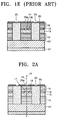
- FIGS. 1A through 1E show a conventional method of manufacturing a VCSEL.
- a lower reflector layer 13, an active layer 15, a pre-oxidized layer 17, and an upper reflector layer 19 are sequentially stacked on a substrate 10'.
- the substrate 10' is formed of, for example, a semiconductor material containing n-type impurities.
- the lower reflector layer 13 is doped with impurities of the same type as the substrate 10 and is formed, for example, by stacking 20-30 layers of n-type GaAs, in which the ratio of Ga to As is different in each layer, on the substrate 10'.
- the upper reflector layer 19 is formed of the same semiconductor material as the lower reflector layer 13 but contains the opposite type of impurities to those contained in the lower reflector layer 13. In other words, the upper reflector layer 19 is formed of p-type GaAs.
- the pre-oxidized layer 17 is subjected to a horizontal oxidation process in vapor.
- a dry etching process is performed to form spaces 21, thereby forming a plurality of VCSEL posts I, II and III on the substrate 10 through each of which light will be independently radiated.
- the pre-oxidized layer 17 is oxidized horizontally from its outside to its inside, thereby forming a horizontally oxidized high-resistance portion 18 and a current aperture 17 which is not oxidized, as shown in FIG. 1C.
- the spaces 21 are filled with polyimide 23 in order to prevent posts from being damaged during a lapping process on the substrate 10'. Then, the polyimide 23 filling the spaces 21 is planarized to be level with the surroundings. Thereafter, the resultant structure is turned over and most of the substrate 10 is removed by a lapping process.
- an upper electrode 25 having a window 25a is formed on the VCSEL posts I, II and III and the polyimide 23, and a lower electrode 27 is formed on the bottom surface of a lapped substrate 10', thereby completing the manufacture of a VCSEL.
- VCSELs having the above structure may be used as a single chip array structure, or may be cut at each polyimide portion so as to be used separately.
- a VCSEL may be designed by way of “electrode pulling" in which upper electrodes 25 are formed beyond the region of the current aperture 17 between high-resistance portions 18, as shown in FIG. 2B.
- the current path 30 is lengthened, thereby increasing overall device resistance.
- an upper electrode window size 34 is formed smaller than a current aperture size 32, so a loss of emitted light occurs.
- the present invention provides a semiconductor light-emitting device having a post which is composed of a plurality of layers (13, 15, 17, 19) including at least one pre-oxidized layer (17) on a substrate (10), and an electrode (36) on the post, characterized in that the semiconductor light-emitting device is manufactured by forming the post by performing etching by way of self-alignment using the electrode (36), and horizontally oxidizing the pre-oxidized layer (17) a predetermined distance from a sidewall of the post.
- the post is formed by performing etching by way of self-alignment using the electrode in order to align the central axes of the respective electrode window and the current aperture, which are formed within the post.
- the sidewall of a pre-oxidized layer included in the post is exposed, and the pre-oxidized layer is horizontally oxidized by an oxidizing process by a predetermined distance from the sidewall thereof.
- the diameter of the post is about 60 ⁇ m
- about 45-50 ⁇ m of the pre-oxidized layer is oxidized.
- a portion of the pre-oxidized layer oxidized by the oxidizing process becomes a high-resistance portion, and a portion of the pre-oxidized layer unoxidized during the oxidizing process becomes a current aperture through which current or light passes.
- the post is formed by way of self-alignment using the electrode, and the current aperture is formed by oxidizing the exposed sidewall of the post, the central axis of the window of the electrode and the central axis of the current aperture are automatically aligned. Therefore, due to the exact alignment between the window and the current aperture, the electro-optical characteristics of the Vertical Cavity Surface Emitting Laser (VCSEL) are improved.
- VCSEL Vertical Cavity Surface Emitting Laser
- the window of the electrode is passivated by photoresist in order to avoid damage occurring during etching performed by way of self-alignment using the electrode.
- the surface of the electrode is partially or entirely passivated by the photoresist.
- the surface of the electrode is partially passivated, even if a portion of the electrode exposed during the etching process is damaged, the remaining portion of the electrode protected by the photoresist is sufficient to demonstrate conductivity as an electrode.
- the present invention provides a method of manufacturing a semiconductor light-emitting device including a substrate (10) and a lower reflector layer (13), an active layer (15), a pre-oxidized layer (17), and an upper reflector layer (19) which are sequentially formed on the surface of the substrate (10) characterized in that the method comprises the steps of:
- the present invention provides a method of manufacturing a semiconductor light-emitting device including a substrate (10) and a lower reflector layer (13), an active layer (15), a pre-oxidized layer (17), and an upper reflector layer (19) which are sequentially formed on the surface of the substrate (10), characterized in that the method comprises the steps of:
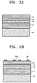
- FIG. 3A shows a stacked semiconductor structure used for manufacturing a semiconductor light-emitting device (hereinafter, referred to as a Vertical Cavity Surface Emitting Laser (VCSEL)) according to a preferred embodiment of the present invention.
- the VCSEL has a stacked semiconductor structure in which light is emitted in a direction perpendicular to the plane of a layer.
- Such a stacked semiconductor structure is formed by epitaxial deposition such as Metal-Organic Chemical Vapor Deposition (MOCVD), Liquid Phase Epitaxy (LPE), Molecular Beam Epitaxy (MBE), or other well-known crystal growth methods.
- MOCVD Metal-Organic Chemical Vapor Deposition
- LPE Liquid Phase Epitaxy
- MBE Molecular Beam Epitaxy
- the stacked semiconductor structure includes a substrate 10, a lower reflector layer 13, an active layer 15, a pre-oxidized layer 17, and an upper reflector layer 19, from the bottom to the top.
- the substrate 10 prepared first in manufacturing a VCSEL is, for example, an n-type GaAs substrate having a high concentration of impurities.
- the impurity concentration is, for example, 5x10 18 cm -3 .
- the GaAs substrate facilitates epitaxial deposition of AlGaAs or AlAs as will be described later.
- the lower reflector layer 13 is formed on the substrate 10.
- a semiconductor buffer layer such as a GaAs thin film of about 0.5 ⁇ m which can be epitaxially deposited on the substrate 10 may be formed before the lower reflector layer 13 is formed.
- the lower reflector layer 13 is formed of a distributed Bragg reflector (DBR) having the same conductivity as the substrate 10, that is, an n-type, in a superlattice structure.
- the lower reflector layer 13 is formed on the substrate 10 by epitaxial deposition such as MOCVD and/or MBE.
- the lower reflector layer 13 performs internal reflection in a VCSEL structure.
- a plurality of Al x Ga 1-x As layers and a plurality of Al y Ga 1-y As layers are alternately stacked.
- Each Al y Ga 1-y As layer has a low aluminium content of, for example, about 10%, so that it usually has a predetermined refractive index.
- Each Al x Ga 1-x As layer has a high aluminium content of, for example, about 95%.
- each alternating layer constituting the lower reflector layer 13 has an effective optical thickness of about 1/4 of a wavelength of light generated by the VCSEL.
- the lower reflector layer 13 has a reflectance of about 100% as a whole, if possible, in order to achieve high internal reflection in the VCSEL.
- the reflectance of the lower reflector layer 13 depends on a difference in the refractive index between Al x Ga 1-x As and Al y Ga 1-y As and the number of pairs of Al x Ga 1-x As and Al y Ga 1-y As in the lower reflector layer 13. Accordingly, as the difference in refractive index and the number of pairs of alternating layers increase, higher reflectance can be obtained.
- the active layer 15 is formed on the lower reflector layer 13 by epitaxial deposition.
- the active layer 15 includes at least one quantum well layer, a barrier layer surrounding the quantum well layer, and a cladding layer surrounding the barrier layer.
- the barrier layer has a middle energy band gap between the energy band gap of the quantum well layer and the energy band gap of the cladding layer.
- the active layer 15 is designed to provide sufficient optical gain to the VCSEL.
- the active layer 15 is formed by alternately stacking three quantum well layers of In 0.2 Ga 0.8 As each having a thickness of 8 nanometers and barrier layers of GaAs each having a thickness of 10 nanometers and surrounding each quantum well layer, and forming cladding layers of Al 0.5 Ga 0.8 As so that the stack of quantum well layers and barrier layers are sandwiched between the cladding layers.
- a quantum well layer, a barrier layer, and a cladding layer are not discriminated but are illustrated as a single layer in order to simplify the drawings.
- the pre-oxidized layer 17 is formed on the active layer 15 by epitaxial deposition.
- the pre-oxidized layer 17 is doped with the same type of dopant as the nearest reflector layer. Since the pre-oxidized layer 17 is positioned between the active layer 15 and the upper reflector layer 19, preferably the pre-oxidized layer 17 is doped with the same type of dopant as the upper reflector layer 19.
- the pre-oxidized layer 17 is doped with a p-type dopant at concentration of about 10 18 cm -3 .
- the pre-oxidized layer 17 includes posts and a semiconductor alloy containing aluminium, for example, AlAs or AlGaAs, which can be partially oxidized after a post is formed.
- the pre-oxidized layer 17 is oxidized starting from the sidewall of each post formed by the etching process, toward the inside so that an oxidized portion usually has a circular shape.
- the shape of the oxidized portion will depend on the shape of the post and the number of sidewalls exposed in an oxidizing process.
- the shape of an oxidized portion can be influenced or controlled by the composition of a semiconductor alloy contained in the pre-oxidized layer 17, the orientation of the alloy, the thickness of the pre-oxidized layer 17, and the conditions of the oxidizing process. For example, during an oxidizing process, aqueous vapor contained in N 2 carrier gas oxidizes AlAs at a temperature of 400-500°C, thereby forming aluminium oxide.
- AlAs containing 100% Al is oxidized by about 1.5 ⁇ m per minute at 450°C
- AlGaAs containing 80% Al is oxidized by about 0.01 ⁇ m per minute.
- U.S. Patent Nos. 5,262,360 and 5,373,522 issued to Holonyak, Jr. et al. and U.S. Patent No. 5,493,577 issued to Choquette et al. can be referred to for more details about the shape of an oxidized portion and the conditions of a proper process.
- the upper reflector layer 19 is formed on the pre-oxidized layer 17 by epitaxial deposition. Like the lower reflector layer 13, the upper reflector layer 19 is formed by alternately stacking a plurality of Al x Ga 1-x As layers and a plurality of Al y Ga 1-y As layers. However, the upper reflector layer 19 is doped with impurities of a different conductivity than the lower reflector layer 13. In other words, when the lower reflector layer 13 and the substrate 10 are doped with an n-type dopant, the upper reflector layer 19 is preferably doped with a p-type dopant. In addition, the upper reflector layer 19 is designed to have a smaller number of layers than the lower reflector layer 13 in order to reduce its reflectance to allow the VCSEL to emit light. The preferred upper reflector layer 19 usually has a reflectance of 98-99%.
- the active layer 15 and the pre-oxidized layer 17 are sandwiched between the lower reflector layer 13 and the upper reflector layer 19. Therefore, the upper reflector layer 19 and the lower reflector layer 13 form a resonant surface for resonating light generated from the active layer 15.
- an upper electrode 36 is formed on the upper reflector layer 19 of the resultant structure of FIG. 3A.
- the upper electrode 36 is formed by depositing, for example, AuBe/Ti/Au metal or Cr/Au metal on the p-type upper reflector layer 19, and has a window 25a formed at a predetermined position by a photolithographic masking process or a lift-off process.
- photoresist 38 is patterned around the window 25a, as shown in FIG. 3C. It is preferable that the photoresist 38 is blanket-deposited over the upper electrode 36 and the window 25a, because an exposed upper electrode is likely to be damaged during a later etching process. However, it will be fine even if a part of an electrode is exposed, as shown in FIG. 3C, taking into account an error in patterning photoresist because the remaining part of the electrode is sufficiently protected by the photoresist to maintain conductivity as an electrode.
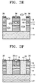
- an etching process is performed using the upper electrode 36 and the photoresist 38 as a mask, thereby forming spaces 40 and posts of a mesa type. Through such a process of forming posts, edges of the stacked materials are exposed. Wet or dry etching performs the post forming process. It is preferable to use dry etching such as reactive ion etching (RIE) in order to obtain a sidewall of accurate depth and uniform surface. RIE is disclosed in detail in U.S. Patent No. 5,034,092, entitled “Plasma Etching of Semiconductor Substrates", issued 23 July 1991.
- RIE reactive ion etching
- RIE Reactive Ion Beam Etching
- CAIBE Chemically Assisted Ion Beam Etching
- IBAGSC Ion Beam Activated Gas Surface Chemistry
- an accurate etching depth can be provided by an in-situ process using a reflected light measuring apparatus, and the etching process can be stopped after the pre-oxidized layer 17 is etched downward.
- an oxidizing process is performed on the pre-oxidized layer 17 formed of, for example, AlAs, as shown in FIG. 3E.
- Such an oxidizing process was proposed for the first time in U.S. Patent No. 5,262,360, issued to Holonyak, Jr. et al., entitled “AlGaAs Native Oxide", filed 24 June 1991 and patented 16 November 1993.
- an aluminum-containing Group III-V semiconductor material is exposed to a water-containing environment at a temperature of about 375°C to convert at least a portion of the aluminium-containing material into a native oxide.
- U.S. Patent No. 5,373,522 issued to Holonyak, Jr. et al., entitled “Semiconductor Devices with Native Aluminium Oxide Regions", filed 7 September 1993 and patented 13 December 1994, claims the structure of a semiconductor laser using the oxidizing method disclosed in U.S. Patent No. 5,262,360.
- a native oxide formed from aluminium according to U.S. Patent No. 5,262,360 is used as a current blocking layer within a semiconductor laser.
- the selective oxidizing process performed in the preferred embodiment and the current aperture formed by the selective oxidizing process are based on the above documents.
- a selective oxidizing process is performed by positioning a VCSEL wafer in a container and heating the wafer in a controlled environment maintaining a high percentage of humidity, preferably, at a temperature of 350-500°C, and more preferably, at a temperature of 400-450°C.
- the pre-oxidized layer 17 is horizontally oxidized from the sidewall of each etched post toward the center of the post. Meanwhile, the layers other than the pre-oxidized layer 17 in the stack structure are not oxidized because their aluminium content is small.
- An oxidized portion 18 of the pre-oxidized layer 17 subjected to the selective etching method usually has a circular shape, electrically high resistance or insulation, and a low refractive index of about 1.6.
- An unoxidized portion 17 of the pre-oxidized layer 17 becomes a passage through which light is emitted and a current aperture through which electric current flows.
- the oxidized portion 18 surrounding the current aperture has a donut shape when viewed from above the post.
- the bottom of the substrate 10 is lapped in order to facilitate cutting of the wafer.
- a lower electrode 27 is formed by depositing patterned AuGe/Ni/Au on the entire bottom surface of the lapped substrate 10' or by blanket-metalizing the bottom surface of the lapped substrate 10'.
- the lower electrode 27 is annealed together with the upper electrode 36, thereby becoming an electrode portion of the VCSEL.
- the lower electrode 27 includes opaque metals or semitransparent metals.
- the lower electrode 27 has a multi-layer structure including AuGe having a thickness of about 800 ⁇ , Ni having a thickness of about 200 ⁇ and Au having a thickness of about 400 ⁇ .
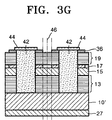
- a wire bonding pad 44 is formed on the upper electrode 36 that has been used as a mask to form the post, thereby completing a VCSEL array, as shown in FIG. 3G.
- VCSELs manufactured through the above steps may be used as a single chip array structure or may be cut at each polyimide portion to be used separately.
- a post is formed first, and then a window of an upper electrode is formed to correspond to a current aperture formed by oxidizing a pre-oxidized layer, so it is difficult to align the central axis of the window of the upper electrode and the central axis of the current aperture. As a result, an alignment error occurs, thereby deteriorating the electro-optical characteristics of a VCSEL.
- the preferred embodiment forms an upper electrode first, forms a post by performing an etching process using the upper electrode, and forms a current aperture using an oxidizing process, so the central axis of the window of the upper electrode and the central axis of the current aperture are self-aligned. Accordingly, such a VCSEL has improved electro-optical characteristics due to the exact alignment between the central axis of a window of an upper electrode and the central axis of a current aperture, compared to a conventional VCSEL.
- At least one current aperture can be formed above and/or below the active layer in order to control the optical characteristics of the VCSEL.
- the present invention has been described with reference to a method of manufacturing a post having a circular shape when viewed in a direction in which light is emitted from a VCSEL to achieve circular light emission, the present invention can be applied to a post having a rectangular, square, elliptical, or other shape, rather than a circular shape according to the use of emitted light.
- photoresist is formed on a part or on the entire surface of an electrode and is then etched to form a post in the above-described embodiment of the present invention, the etching process may be performed after sidewalls are formed at both opposite ends of the electrode.
Landscapes
- Physics & Mathematics (AREA)
- Condensed Matter Physics & Semiconductors (AREA)
- General Physics & Mathematics (AREA)
- Electromagnetism (AREA)
- Optics & Photonics (AREA)
- Semiconductor Lasers (AREA)
- Led Devices (AREA)
Abstract
Description
Claims (7)
- A semiconductor light-emitting device having a post which is composed of a plurality of layers (13, 15, 17, 19) including at least one pre-oxidized layer (17) on a substrate (10), and an electrode (36) on the post, characterized in that the semiconductor light-emitting device is manufactured by forming the post by performing etching by way of self-alignment using the electrode (36), and horizontally oxidizing the pre-oxidized layer (17) by a predetermined distance from a sidewall of the post.
- The semiconductor light-emitting device of claim 1, wherein the post comprises a lower reflector layer (13), an active layer (15), a pre-oxidized layer (17), and an upper reflector layer (19) which are formed by epitaxial deposition on the substrate (10).
- The semiconductor light-emitting device of claim 1 or 2, wherein the semiconductor light-emitting device is a vertical cavity surface emitting laser which emits light perpendicularly to the plane of a stacked layer.
- The semiconductor light-emitting device of claim 1 or 2, wherein a portion of the pre-oxidized layer (17) is horizontally oxidized, thereby forming a high-resistance portion (18), and an unoxidized portion becomes a current aperture (17) through which current or light passes.
- A method of manufacturing a semiconductor light-emitting device including a substrate (10) and a lower reflector layer (13), an active layer (15), a pre-oxidized layer (17), and an upper reflector layer (19) which are sequentially formed on the surface of the substrate (10), characterised in that the method comprises the steps of:Patterning an upper electrode (36) having a window (25a) on the upper reflector layer (19);forming photoresist (38) on a portion of the upper electrode (36) including the window (25a);performing an etching process using the upper electrode (36) and the photoresist (38) as a mask until the pre-oxidized layer (17) is exposed, thereby forming a post;oxidizing a portion of the pre-oxidized layer (17); andfilling an etched portion resulting from the etching process with a buffer material (42) and forming a lower electrode (27) on the bottom of the substrate (10).
- A method of manufacturing a semiconductor light-emitting device including a substrate (10) and a lower reflector layer (13), an active layer (15), a pre-oxidized layer (17), and an upper reflector layer (19) which are sequentially formed on the surface of the substrate (10), characterized in that the method comprises the steps of:patterning an upper electrode (36) having a window (25a) on the upper reflector layer (19);forming photoresist (38) on the entire surface of the upper electrode (36) including the window (25a) ;performing an etching process using the photoresist (38) as a mask until the pre-oxidized layer (17) is exposed, thereby forming a post;oxidizing a portion of the pre-oxidized layer (17); andfilling an etched portion resulting from the etching process with a buffer material (42) and forming a lower electrode (27) on the bottom of the substrate (10).
- A semiconductor light-emitting device manufactured according to claim 5 or 6.
Applications Claiming Priority (2)
| Application Number | Priority Date | Filing Date | Title |
|---|---|---|---|
| KR1020000078543A KR100708107B1 (en) | 2000-12-19 | 2000-12-19 | Semiconductor light emitting device with improved electro-optic characteristics and manufacturing method thereof |
| KR2000078543 | 2000-12-19 |
Publications (2)
| Publication Number | Publication Date |
|---|---|
| EP1217702A2 true EP1217702A2 (en) | 2002-06-26 |
| EP1217702A3 EP1217702A3 (en) | 2003-05-21 |
Family
ID=19703263
Family Applications (1)
| Application Number | Title | Priority Date | Filing Date |
|---|---|---|---|
| EP01128006A Withdrawn EP1217702A3 (en) | 2000-12-19 | 2001-11-24 | Semiconductor light-emitting device with improved electro-optical characteristics and method of manufacturing the same |
Country Status (6)
| Country | Link |
|---|---|
| US (1) | US6689631B2 (en) |
| EP (1) | EP1217702A3 (en) |
| JP (1) | JP3748807B2 (en) |
| KR (1) | KR100708107B1 (en) |
| CN (1) | CN1173442C (en) |
| TW (1) | TW531905B (en) |
Cited By (2)
| Publication number | Priority date | Publication date | Assignee | Title |
|---|---|---|---|---|
| GB2386756A (en) * | 2001-12-07 | 2003-09-24 | Agilent Technologies Inc | Planar index guided VCSEL |
| GB2399221A (en) * | 2003-02-06 | 2004-09-08 | Agilent Technologies Inc | Oxide vertical cavity surface-emitting laser |
Families Citing this family (37)
| Publication number | Priority date | Publication date | Assignee | Title |
|---|---|---|---|---|
| US7279718B2 (en) * | 2002-01-28 | 2007-10-09 | Philips Lumileds Lighting Company, Llc | LED including photonic crystal structure |
| JP4062983B2 (en) * | 2002-06-20 | 2008-03-19 | 富士ゼロックス株式会社 | Surface emitting semiconductor laser and manufacturing method thereof |
| TWI222756B (en) * | 2002-11-12 | 2004-10-21 | Epitech Corp Ltd | Lateral current blocking light emitting diode and method of making the same |
| TW565975B (en) * | 2002-12-27 | 2003-12-11 | Ind Tech Res Inst | Oxide confined type vertical cavity surface emitting laser device and the manufacturing method thereof |
| JP4138629B2 (en) * | 2003-11-06 | 2008-08-27 | 株式会社東芝 | Surface emitting semiconductor device and manufacturing method thereof |
| CN1305191C (en) * | 2004-04-06 | 2007-03-14 | 北京工业大学 | Prepn. of inner chanber contacting vertical chamber emitting laser by 3-shaft self-aligning process |
| CN100413102C (en) * | 2004-04-30 | 2008-08-20 | 住友电气工业株式会社 | semiconductor light emitting device |
| KR100710048B1 (en) * | 2004-12-14 | 2007-04-23 | 한국전자통신연구원 | Semiconductor laser diode and a method for manufacturing the same |
| US7459719B2 (en) * | 2004-12-17 | 2008-12-02 | Panasonic Corporation | Superlattice optical semiconductor device where each barrier layer has high content of group III elements in center portion and low content near well layer |
| JP4483728B2 (en) * | 2005-07-19 | 2010-06-16 | 住友電気工業株式会社 | Manufacturing method of semiconductor optical device |
| US20070212507A1 (en) * | 2006-03-13 | 2007-09-13 | Arst Kevin M | Document Flagging And Indexing System |
| US7425465B2 (en) * | 2006-05-15 | 2008-09-16 | Fujifilm Diamatix, Inc. | Method of fabricating a multi-post structures on a substrate |
| US7820540B2 (en) * | 2007-12-21 | 2010-10-26 | Palo Alto Research Center Incorporated | Metallization contact structures and methods for forming multiple-layer electrode structures for silicon solar cells |
| KR101033523B1 (en) * | 2008-11-10 | 2011-05-09 | 고려대학교 산학협력단 | Linear Solar Concentrators and Their Applications |
| US8270447B2 (en) * | 2009-01-08 | 2012-09-18 | Furukawa Electric Co., Ltd. | Semiconductor light emitting element and manufacturing method thereof |
| JP2011258741A (en) * | 2010-06-09 | 2011-12-22 | Fuji Xerox Co Ltd | Optical transmission device |
| TWI559570B (en) * | 2011-05-31 | 2016-11-21 | 晶元光電股份有限公司 | Light-emitting device |
| US9435641B2 (en) * | 2013-06-20 | 2016-09-06 | Analog Devices, Inc. | Optical angle measurement |
| US9274202B2 (en) | 2013-06-20 | 2016-03-01 | Analog Devices, Inc. | Optical time-of-flight system |
| TWI664746B (en) * | 2015-06-17 | 2019-07-01 | 晶元光電股份有限公司 | Semiconductor light-emitting device |
| US10153615B2 (en) | 2015-07-30 | 2018-12-11 | Optipulse, Inc. | Rigid high power and high speed lasing grid structures |
| US10630053B2 (en) | 2015-07-30 | 2020-04-21 | Optipulse Inc. | High power laser grid structure |
| CN108269821A (en) * | 2016-12-30 | 2018-07-10 | 英属开曼群岛商錼创科技股份有限公司 | Show equipment |
| US11835626B2 (en) | 2017-01-10 | 2023-12-05 | Samsung Electronics Co., Ltd. | Fabry-Perot cavity phase modulator including a tunable core, an optical modulating device including the same, and a lidar apparatus including the optical modulating device |
| US20180196138A1 (en) * | 2017-01-10 | 2018-07-12 | Samsung Electronics Co., Ltd. | Optical modulating device and system including the same |
| US10958350B2 (en) | 2017-08-11 | 2021-03-23 | Optipulse Inc. | Laser grid structures for wireless high speed data transfers |
| US10374705B2 (en) | 2017-09-06 | 2019-08-06 | Optipulse Inc. | Method and apparatus for alignment of a line-of-sight communications link |
| US11233377B2 (en) * | 2018-01-26 | 2022-01-25 | Oepic Semiconductors Inc. | Planarization of backside emitting VCSEL and method of manufacturing the same for array application |
| DE102019116862B4 (en) | 2018-08-29 | 2021-09-30 | Taiwan Semiconductor Manufacturing Co. Ltd. | TECHNIQUES FOR OXIDATING SURFACE-EMITTING LASERS WITH VERTICAL CAVITY |
| US10847949B2 (en) * | 2018-08-29 | 2020-11-24 | Taiwan Semiconductor Manufacturing Co., Ltd. | Techniques for vertical cavity surface emitting laser oxidation |
| CN109088309B (en) * | 2018-10-16 | 2024-01-26 | 厦门乾照半导体科技有限公司 | High-frequency vertical cavity surface emitting laser chip and preparation method thereof |
| CN110970538B (en) * | 2019-11-22 | 2022-03-15 | 深圳市思坦科技有限公司 | Red light LED epitaxial wafer, division method of LED epitaxial wafer and structure of LED epitaxial wafer |
| WO2021124967A1 (en) * | 2019-12-20 | 2021-06-24 | ソニーグループ株式会社 | Vertical cavity surface-emitting laser element, vertical cavity surface-emitting laser element array, vertical cavity surface-emitting laser module, and method for manufacturing vertical cavity surface-emitting laser element |
| US20220171027A1 (en) * | 2020-11-27 | 2022-06-02 | Samsung Electronics Co., Ltd. | Spatial light modulator, lidar apparatus including the same, and method of manufacturing the spatial light modulator |
| CN113572021B (en) * | 2021-07-22 | 2022-06-21 | 上海新微半导体有限公司 | Self-aligning preparation method for front electrode window of DFB laser |
| CN117096725A (en) * | 2022-05-12 | 2023-11-21 | 常州承芯半导体有限公司 | Vertical cavity surface emitting laser and method of forming the same |
| CN114927938A (en) * | 2022-05-18 | 2022-08-19 | 苏州长瑞光电有限公司 | Method for manufacturing vertical cavity surface emitting laser and vertical cavity surface emitting laser |
Family Cites Families (8)
| Publication number | Priority date | Publication date | Assignee | Title |
|---|---|---|---|---|
| US5034092A (en) | 1990-10-09 | 1991-07-23 | Motorola, Inc. | Plasma etching of semiconductor substrates |
| US5262360A (en) | 1990-12-31 | 1993-11-16 | The Board Of Trustees Of The University Of Illinois | AlGaAs native oxide |
| US5116461A (en) | 1991-04-22 | 1992-05-26 | Motorola, Inc. | Method for fabricating an angled diffraction grating |
| EP0542479A1 (en) * | 1991-11-15 | 1993-05-19 | AT&T Corp. | Method of making a semiconductor laser |
| US6156582A (en) * | 1993-06-14 | 2000-12-05 | Motorola, Inc. | Method of fabricating top emitting ridge VCSEL with self-aligned contact and sidewall reflector |
| US5493577A (en) | 1994-12-21 | 1996-02-20 | Sandia Corporation | Efficient semiconductor light-emitting device and method |
| KR100462425B1 (en) * | 1995-11-27 | 2005-04-28 | 스미또모 가가꾸 가부시키가이샤 | Group 3-5 compound semiconductor and light emitting device |
| US5719891A (en) * | 1995-12-18 | 1998-02-17 | Picolight Incorporated | Conductive element with lateral oxidation barrier |
-
2000
- 2000-12-19 KR KR1020000078543A patent/KR100708107B1/en not_active Expired - Fee Related
-
2001
- 2001-10-19 TW TW090125890A patent/TW531905B/en not_active IP Right Cessation
- 2001-11-09 CN CNB011378956A patent/CN1173442C/en not_active Expired - Fee Related
- 2001-11-22 JP JP2001358442A patent/JP3748807B2/en not_active Expired - Fee Related
- 2001-11-24 EP EP01128006A patent/EP1217702A3/en not_active Withdrawn
- 2001-12-14 US US10/014,884 patent/US6689631B2/en not_active Expired - Fee Related
Cited By (4)
| Publication number | Priority date | Publication date | Assignee | Title |
|---|---|---|---|---|
| GB2386756A (en) * | 2001-12-07 | 2003-09-24 | Agilent Technologies Inc | Planar index guided VCSEL |
| GB2386756B (en) * | 2001-12-07 | 2005-10-12 | Agilent Technologies Inc | Planar index-guided vcsel |
| GB2399221A (en) * | 2003-02-06 | 2004-09-08 | Agilent Technologies Inc | Oxide vertical cavity surface-emitting laser |
| GB2399221B (en) * | 2003-02-06 | 2005-12-14 | Agilent Technologies Inc | Oxide vertical cavity surface-emitting laser |
Also Published As
| Publication number | Publication date |
|---|---|
| US6689631B2 (en) | 2004-02-10 |
| EP1217702A3 (en) | 2003-05-21 |
| KR100708107B1 (en) | 2007-04-16 |
| KR20020049385A (en) | 2002-06-26 |
| CN1360376A (en) | 2002-07-24 |
| JP3748807B2 (en) | 2006-02-22 |
| TW531905B (en) | 2003-05-11 |
| CN1173442C (en) | 2004-10-27 |
| US20020109149A1 (en) | 2002-08-15 |
| JP2002223034A (en) | 2002-08-09 |
Similar Documents
| Publication | Publication Date | Title |
|---|---|---|
| US6689631B2 (en) | Semiconductor light-emitting device with improved electro-optical characteristics and method of manufacturing the same | |
| US8497141B2 (en) | Semiconductor device and method of manufacturing it | |
| CN113228434B (en) | Vertical Cavity Surface Emitting Laser | |
| US7098059B2 (en) | Surface emitting semiconductor laser and process for producing the same including forming an insulating layer on the lower reflector | |
| JP4359345B2 (en) | Passivated vertical cavity surface emitting laser. | |
| US6160833A (en) | Blue vertical cavity surface emitting laser | |
| US5446752A (en) | VCSEL with current blocking layer offset | |
| KR100449768B1 (en) | Hybrid mirror structure for visible emission VCSEL | |
| JP2002353563A (en) | Semiconductor light emitting device and method of manufacturing the same | |
| CN211929898U (en) | Vertical cavity surface emitting laser device | |
| JP3800856B2 (en) | Surface emitting laser and surface emitting laser array | |
| JP2021009999A (en) | Surface emitting laser and method for manufacturing the same | |
| JPH06314854A (en) | Surface light emitting element and its manufacture | |
| CN112152073B (en) | Surface emitting laser | |
| JP4224981B2 (en) | Surface emitting semiconductor laser device and method for manufacturing the same | |
| US6795457B2 (en) | Multiple wavelength surface-emitting laser device and method for its manufacture | |
| JP2001244560A (en) | Semiconductor light emitting device manufacturing method and semiconductor light emitting device | |
| JP3685541B2 (en) | Semiconductor laser device and manufacturing method thereof | |
| US11539188B2 (en) | Surface emitting laser and method of manufacturing the same | |
| JPH07312462A (en) | Method for manufacturing surface emitting laser diode and surface emitting laser diode | |
| JPH09205250A (en) | Lateral current injection type surface emitting semiconductor laser device and its manufacture | |
| JPH10200187A (en) | Surface emitting semiconductor laser and method of manufacturing the same | |
| JPH04216691A (en) | Semiconductor laser device and its manufacture | |
| KR100446604B1 (en) | SINGLE LATITUDINAL MODE GaN-BASED PLANE LIGHT EMITTING LASER DIODE INCLUDING LOWER DISTRIBUTED BRAGG REFLECTOR FORMED OF PAIRS OF GaN LAYERS AND AIR LAYERS AND UPPER DISTRIBUTED BRAGG REFLECTOR FORMED OF PAIRS OF DIELECTRIC LAYERS, AND METHOD FOR MANUFACTURING THE SAME | |
| KR100272129B1 (en) | A gan based emitting semiconductor laser diode with single mode operation and a fabrication method thereof. |
Legal Events
| Date | Code | Title | Description |
|---|---|---|---|
| PUAI | Public reference made under article 153(3) epc to a published international application that has entered the european phase |
Free format text: ORIGINAL CODE: 0009012 |
|
| 17P | Request for examination filed |
Effective date: 20011205 |
|
| AK | Designated contracting states |
Kind code of ref document: A2 Designated state(s): AT BE CH CY DE DK ES FI FR GB GR IE IT LI LU MC NL PT SE TR |
|
| AX | Request for extension of the european patent |
Free format text: AL;LT;LV;MK;RO;SI |
|
| PUAL | Search report despatched |
Free format text: ORIGINAL CODE: 0009013 |
|
| AK | Designated contracting states |
Designated state(s): AT BE CH CY DE DK ES FI FR GB GR IE IT LI LU MC NL PT SE TR |
|
| AX | Request for extension of the european patent |
Extension state: AL LT LV MK RO SI |
|
| AKX | Designation fees paid |
Designated state(s): DE FR GB |
|
| 17Q | First examination report despatched |
Effective date: 20090309 |
|
| STAA | Information on the status of an ep patent application or granted ep patent |
Free format text: STATUS: THE APPLICATION IS DEEMED TO BE WITHDRAWN |
|
| 18D | Application deemed to be withdrawn |
Effective date: 20090721 |