EP1217426A1 - Method for manufacturing transmission screen and transmission screen - Google Patents
Method for manufacturing transmission screen and transmission screen Download PDFInfo
- Publication number
- EP1217426A1 EP1217426A1 EP01945808A EP01945808A EP1217426A1 EP 1217426 A1 EP1217426 A1 EP 1217426A1 EP 01945808 A EP01945808 A EP 01945808A EP 01945808 A EP01945808 A EP 01945808A EP 1217426 A1 EP1217426 A1 EP 1217426A1
- Authority
- EP
- European Patent Office
- Prior art keywords
- light
- lens
- transmissive screen
- compositions
- producing
- Prior art date
- Legal status (The legal status is an assumption and is not a legal conclusion. Google has not performed a legal analysis and makes no representation as to the accuracy of the status listed.)
- Granted
Links
Images




Classifications
-
- G—PHYSICS
- G03—PHOTOGRAPHY; CINEMATOGRAPHY; ANALOGOUS TECHNIQUES USING WAVES OTHER THAN OPTICAL WAVES; ELECTROGRAPHY; HOLOGRAPHY
- G03B—APPARATUS OR ARRANGEMENTS FOR TAKING PHOTOGRAPHS OR FOR PROJECTING OR VIEWING THEM; APPARATUS OR ARRANGEMENTS EMPLOYING ANALOGOUS TECHNIQUES USING WAVES OTHER THAN OPTICAL WAVES; ACCESSORIES THEREFOR
- G03B21/00—Projectors or projection-type viewers; Accessories therefor
- G03B21/54—Accessories
- G03B21/56—Projection screens
- G03B21/60—Projection screens characterised by the nature of the surface
- G03B21/62—Translucent screens
- G03B21/625—Lenticular translucent screens
-
- G—PHYSICS
- G02—OPTICS
- G02B—OPTICAL ELEMENTS, SYSTEMS OR APPARATUS
- G02B3/00—Simple or compound lenses
- G02B3/0006—Arrays
- G02B3/0037—Arrays characterized by the distribution or form of lenses
- G02B3/005—Arrays characterized by the distribution or form of lenses arranged along a single direction only, e.g. lenticular sheets
-
- G—PHYSICS
- G02—OPTICS
- G02B—OPTICAL ELEMENTS, SYSTEMS OR APPARATUS
- G02B3/00—Simple or compound lenses
- G02B3/0006—Arrays
- G02B3/0037—Arrays characterized by the distribution or form of lenses
- G02B3/0062—Stacked lens arrays, i.e. refractive surfaces arranged in at least two planes, without structurally separate optical elements in-between
- G02B3/0068—Stacked lens arrays, i.e. refractive surfaces arranged in at least two planes, without structurally separate optical elements in-between arranged in a single integral body or plate, e.g. laminates or hybrid structures with other optical elements
-
- G—PHYSICS
- G02—OPTICS
- G02B—OPTICAL ELEMENTS, SYSTEMS OR APPARATUS
- G02B5/00—Optical elements other than lenses
- G02B5/02—Diffusing elements; Afocal elements
- G02B5/0205—Diffusing elements; Afocal elements characterised by the diffusing properties
- G02B5/021—Diffusing elements; Afocal elements characterised by the diffusing properties the diffusion taking place at the element's surface, e.g. by means of surface roughening or microprismatic structures
Definitions
- the present invention relates to a projection screen technology, and, more particularly, to a method of producing a transmissive screen used as a display screen of, for example, a projection television or a microfilm reader and to the transmissive screen produced by this method.
- the display displays an image by forming an image on a transmissive screen using image light from an image projecting portion.
- This type of transmissive screen is bright when an observer observes the image and has predetermined very small lens members formed thereon so as to increase the viewing angle.
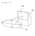
- a viewing angle 1101 which is wider in the horizontal direction than in the vertical direction is preferred. This is because the viewing angle of a human being is wider in the horizontal direction than in the vertical direction.
- the light distribution is made equal in the vertical and horizontal directions, light is also distributed in the vertical direction which is not really necessary with regard to the viewing angle of a human being, so that the brightness as a whole is reduced.
- Representative examples of the structures of the transmissive screen include the following:
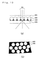
- the planar lens is obtained by forming a sheet comprising a transparent layer, very small transparent balls, and a light-absorption layer, and, then, bonding it to a transparent substrate 1004.
- the lenticular lens it is difficult to achieve a fine pitch when any of the above-described molding methods is performed on thermoplastic resin, so that, when the lenticular lens is used as a screen of a rear projector, which, in recent years, has been providing increasingly higher definition, there is a problem in that deterioration of image quality occurs due to a reduced resolution and production of moiré.
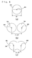
- a very small particles of light diffusing material is usually mixed in the inside portion of the lenticular lens in order to increase the viewing angle in the vertical direction (a direction parallel to the lenticular lens, which is represented by reference numeral 903 in Fig. 9(b)) in which the lenticular lens does not have optical power.
- thermoplastic resin both of the molding methods performed on the thermoplastic resin require large molding machines or dies having diagonals equal to or greater than 50 inches, which are of the same size as the screen of the rear projector, giving rise to the problem that production costs become very high.
- the planar lens is produced by the step of forming a sheet comprising a transparent layer, very small transparent balls, and a light absorption layer, and bonding the sheet to a transparent substrate.
- unevenness in the bonding occurs, so that the display of the image becomes ununiform, and, by insufficient adhesiveness between the sheet and the transparent substrate, interfacial multiple reflection occurs, thereby giving rise to the problem of reduced resolution.
- Means for causing the very small drops of the lens compositions to be discharged and to land is an inkjet recording head.
- the inkjet recording head is a piezo jet recording head.
- the individual lens members, formed on the surface of the transmissive screen are formed by the discharging of lens compositions from an inkjet recording head, typified by, for example, a piezo jet recording head, having the excellent feature of forming a very fine form with high precision over a large area. Therefore, very fine lens members can be produced. Consequently, it is possible to provide a transmissive screen which provides excellent resolution and which does not have a reduced image quality due to moiré.
- this method can be used in producing a transmissive screen by a manufacturing device including a mechanism that makes the piezo jet recording head scan the screen in the horizontal/vertical directions thereof. Therefore, expensive manufacturing devices, such as large dies and molding devices, are not required, thereby making it possible to reduce production costs.
- the surface form of each of the lens members is restricted by adjusting the surface tension and viscosity of each of the lens compositions, and the wettability of each of the lens compositions and a surface which each of the lens compositions contacts.
- a third form of a method of producing a transmissive screen in accordance with the present invention comprises the step of forming the light-absorption-material patterns into the shape of a bank on a surface of the light-transmissive substrate prior to forming the lens members and the precursors thereof by causing the very small drops of the lens compositions to be discharged and to land near a light-transmission portion of the bank-shaped light-absorption-material patterns.
- the lens resin compositions are discharged onto the vicinity of the light-transmission portions of the bank-shaped light-absorption-material patterns in order to form the lens members, so that the light-absorption-material patterns and the lens members are aligned with high precision, thereby increasing the light transmittance of the transmissive screen.
- the surface of the light-transmissive substrate on which the light-absorption-material patterns are formed is different from the surface where the lens members are formed.
- the light-absorption-material patterns or precursors thereof are formed by causing very small drops of light-absorption-material pattern compositions to be discharged and to land.
- Means for causing the very small drops of the light-absorption-material pattern compositions to be discharged and to land is an inkjet recording head.
- the inkjet recording head is a piezo jet recording head.
- the light-absorption-material patterns and the lens members can be formed by the method of discharging very small drops and causing them to land, the production process is simplified, thereby making it possible to provide a low-cost transmissive screen.
- the light-absorption-material patterns are formed by discharging the light-absorption-material-pattern compositions from the inkjet recording head, typified by, for example, a piezo jet recording head, having the excellent feature of forming a very fine form with high precision over a large area, it is possible to form very fine light-absorption-material patterns. Therefore, it is possible to provide a transmissive screen which provides excellent resolution and which does not have a reduced image quality due to moiré. Further, this method can be used to produce a transmissive screen by a manufacturing device including a mechanism that makes the piezo jet recording head scan the screen in the horizontal/vertical directions thereof. Therefore, expensive manufacturing devices, such as large dies and molding devices, are not required, thereby making it possible to reduce production costs.
- a sixth form of a method of producing a transmissive screen in accordance with the present invention comprises the step of restricting a planar form of each of the lens members on the surface of the light-transmissive substrate situated at the side where the lens members are formed prior to forming the lens members or the precursors thereof, with the restricting operation being a chemical operation or a restricted form formation operation, which restrict spreading of the lens member compositions on the transparent substrate.
- the forms of the lens members can be controlled without using a die, it is possible to produce a transmissive screen having any viewing angle at a low cost.
- the step of restricting the planar form of each of the lens members is the same as the step of forming the light-absorption-material patterns.
- adjacent lens members are formed of different lens member compositions.
- the different lens member compositions are adjusted so as to not or only slightly mix with each other.
- the adjacent lens member compositions may be those that do not mix easily with each other, it is possible to reduce the distances between the adjacent lens members, so that dead spaces become smaller. Therefore, it is possible to realize a transmissive screen having high light transmittance.
- a form of a transmissive screen is produced by any one of the methods of producing a transmissive screen.
- the individual lens members, formed on the surface of the transmissive screen are formed by the discharging of lens compositions from an inkjet recording head, typified by, for example, a piezo jet recording head, having the excellent feature of forming a very fine form with high precision over a large area. Therefore, very fine lens members can be produced. Consequently, it is possible to provide a transmissive screen which provides excellent resolution and which does not have a reduced image quality due to moiré.
- this method can be used in producing a transmissive screen by a manufacturing device including a mechanism that makes the piezo jet recording head scan the screen in the horizontal/vertical directions thereof. Therefore, expensive manufacturing devices, such as large dies and molding devices, are not required, thereby making it possible to reduce production cost, and, thus, to provide a low-cost transmissive screen.
- spectral characteristics of the light-transmissive substrate, each of the lens members, and each of the light-absorption-material patterns are substantially flat in the visible region.
- the form of the bottom side of each of the lens members is substantially rectangular.
- the bottom side forms of the individual lens members are substantially rectangular, when the individual lens members are subjected to a filling operation carried out with close attention, dead spaces between the individual lens members are not generated. Therefore, it is possible to realize a bright transmissive screen having high light transmittance.
- a fourth form of the transmissive screen of the present invention when the radius of curvature of each of the lens members in a horizontal direction of the transmissive screen is RH and the radius of curvature of each of the lens members in a vertical direction of the transmissive screen is RV, RH ⁇ RV.
- the viewing angle of the transmissive screen in the horizontal direction can be made larger than the viewing angle of the transmissive screen in the vertical direction. Therefore, it is possible to adequately diffuse image light which has passed through the transmissive screen in the proper direction in accordance with the viewing angle characteristic of a human being. Consequently, a bright transmissive screen can be realized.
- WH width of each of the lens members in a horizontal direction thereof
- WV width of each of the lens members in a vertical direction thereof
- the radius of curvature of the larger-width portion of each lens member becomes large and that of the smaller-width portion of each lens member becomes small.
- the smaller radius of curvature corresponds to the larger optical power.
- each lens member by causing the horizontal-direction width of each lens member to be smaller than the vertical-direction width thereof as in this form, the optical power in the horizontal direction becomes larger than that in the vertical direction, so that the viewing angle of the transmissive screen in the horizontal direction can be made larger than that of the transmissive screen in the vertical direction. Therefore, it is possible to adequately diffuse image light which has passed through the transmissive screen in the proper direction in accordance with the viewing angle characteristic of a human being. Consequently, a bright transmissive screen can be realized.
- the distances between adjacent landing target locations of the lens compositions are not uniform in a plane of the transmissive screen.
- the lens members are not disposed at the transmissive screen in a regular manner, it is possible to improve the quality of a projected image with reduced moiré.
- the distances between the adjacent landing target locations of the lens compositions in a horizontal direction and those in a vertical direction are different.
- the distances in the horizontal direction are PH and those in the vertical direction are PV, PH > PV.
- the distances between the adjacent landing target locations of the lens compositions are such that PH > SP > PV.
- the resulting compound lens member obtained is such that its vertical-direction radius of curvature is larger than the horizontal-direction radius of curvature, so that it is possible for the horizontal-direction viewing angle of the transmissive screen to be greater than the vertical-direction viewing angle of the transmissive screen.
- the method comprises the step of forming volume-type phase devices or precursors thereof by causing very small drops of volume-type phase device compositions to be discharged and to land, with the volume-type phase devices having random phase distributions being provided side by side on a surface of the light-transmissive substrate where the lens members are formed or the back side of the surface.
- Means for causing the very small drops of the volume-type phase device compositions to be discharged and to land is an inkjet recording head.
- the inkjet recording head is a piezo jet recording head.
- volume-type phase devices having random phase distribution are provided side by side on the back side of a lens-formation surface of the light-transmissive substrate. Since interference is reduced by randomly disturbing a wave surface of image light, speckles can be considerably reduced.
- the volume-type phase devices are formed by using an inkjet recording head, typified by a piezo jet recording head, production costs can be reduced.
- Fig. 1 illustrates a generalization of the steps used in the first embodiment.
- a light-absorption material 102 is subjected to a patterning operation to assume a desired form on a light-transmissive substrate 101. It is desirable that the light-transmissive substrate 101 have a substantially uniform light transmittance property over the entire visible region and that this light transmittance be high.
- the light-transmissive substrate 101 may be made to have light diffusion property by diffusing very small, diffusing particles of light diffusing material in the substrate or by forming the surface thereof as a diffusing surface.
- the light-absorption material 102 is a material having a substantially uniform absorption property over the entire visible region, and for the light transmittance of the material to be low.
- the characteristics of the material are selected by considering various characteristics from the viewpoints of the patterning method used and chemical interactions between lens members.
- Examples of methods of patterning the light-absorption material 102 are photolithography and various other printing techniques, and a method in which light-absorption material composition is discharged onto selected locations from an inkjet recording head, typified by a piezo jet recording head, but are not limited to a particular method.
- the most preferable method is the method using a piezo jet recording head because, economically speaking, it allows formation of a very fine form over a large area with high precision.
- the light-absorption material 102 is formed at locations selected near boundary portions of individual lens members formed in a later step.
- Fig. 2(a) illustrates the state of arrangement of the light-absorption material 102 in plan view.
- Fig. 2(a) is a plan view in which the transmissive screen used in the embodiment is seen from a side from which image light is incident, with solid lines indicating individual lens members 105 and dotted lines indicating the light-absorption material 102.
- the light-absorption material 102 is provided near the boundary portions of the lens members 105, and open portion 107 passing light rays are formed near the center portions of the lens members 105.
- Fig. 2(b) is a cross-sectional structure of the transmissive screen and an image light path, in a section taken along line H-H' of Fig. 2(a).
- Image light 201 incident upon the lens members 105 is refracted by the lens members 105, passes through the open portions 107, and is transmitted towards an observer.
- most of outside light 202 from, for example, an illumination lamp disposed in the space at the observer side is absorbed by the light-absorption material 102. Therefore, even if the illumination intensity in the space at the observer side is high, it is possible to enjoy observing a sharp black image having high contrast.
- the proportion of image light 201 that is absorbed becomes large. Therefore, in order to increase transmittance of the image light, it is preferable to make the top side width 203 as small as possible.
- the cross-sectional form of the light-absorption material 102 be a tapering form so as to widen towards the light-transmissive substrate 101.
- the open portions 107 are disposed near the focal points of the lens members 105. From this viewpoint, the height of the light-absorption material 102 is determined.
- lens member compositions 108 are discharged into spaces bounded by the light-absorption material 102 from a piezo jet recording head 103 in order to form lens precursors 104.
- the piezo jet recording head 103 discharges the supplied lens member compositions from its nozzle by a known inkjet method. To facilitate understanding of the embodiment, only one head is shown, but it is obvious that productivity can be increased by disposing a plurality of heads side by side in order to discharge the lens member compositions over a large area and by having the plurality of heads scan the entire plane of the light-transmissive substrate 101.
- the spaces bounded by the light-absorption material 102 are filled with drops 108 of the discharged lens member compositions, and the lens member precursors 104 whose surfaces have been formed into the forms of lenses are formed.
- the forms of the surfaces of the precursors 104 are determined primarily by the viscosities and surface tensions of the lens member compositions and the wettability of the lens member compositions with respect to the light-absorption material. From these viewpoints, the chemical composition of the light-absorption material and the lens member compositions are adjusted.
- a boundary width 109 between the adjacent precursors 104 is drawn extremely small, from the viewpoint of forming the forms of the surfaces of the precursors 104, the boundary width 109 may be large. However, when the boundary widths 109 are made too large, the transmittance of the image light- is reduced. From this viewpoint, it is effective-to use a method in which different types of compositions that do not mix easily with each other are used for the lens member compositions that are discharged from adjacent nozzles 103a and 103b. This is because, when this method is used, even if the lens member compositions spread, the boundaries between the lens members are naturally formed as a result of the lens member compositions coming into contact with each other.
- a hydrophilic composition may be used for one of the lens member composition types and a hydrophobic composition may be used for the other type of lens member composition.
- a hydrophilic composition may be used for one of the lens member composition types and a hydrophobic composition may be used for the other type of lens member composition.
- the lens member composition types which may be used are not limited thereto.
- the precursors 104 are formed into the lens members 105 having desired characteristics.
- An example of the post-processing operation may be a hardening reaction by, for example, irradiation of light or heating.
- the type of post processing operation is not limited thereto, so that various other types of post-processing operations may be carried out based on the chemical properties of the lens member compositions used.
- the post processing step includes not only a hardening reaction, but also post-processing for increasing light transmittance, post-processing for forming the precursors 104 into more desirable forms, etc.
- the post-processing step is omitted.
- An example of such a case is that compositions which react chemically by mixing two liquids or anaerobic compositions are used as the lens member compositions.
- Fig. 1(d) shows an example in which a transparent protective layer 106 is provided at the surface of each lens member in order to increase the mechanical strength of the transmissive screen.
- additional characteristics include, in addition to mechanical strength, increased chemical durability by, for example, anaerobic processing, and the increased optical characteristics based on, for example, AR coating.
- Fig. 3 illustrates the structure of a lens member used in the embodiment.
- Fig. 3(a) shows the bottom surface form (the form of the surface that contacts the light-transmissive substrate 101) of the lens member 105, in which, when its horizontal-direction width 301 is WH and its vertical-direction width 302 is WV, WH ⁇ WV.
- a bottom surface form is determined by the planar form of the light-absorption material 102.
- the form of the surface of the lens member 105 is determined primarily by the viscosity and surface tension of the lens member composition and the wettability of the lens member composition with respect to the light-absorption material, so that when a horizontal-direction radius of curvature 303 of the surface of the lens member 105 along line H-H' shown in Fig. 3(a) is RH and a vertical-direction radius of curvature 304 of the surface of the lens member 105 taken along line V-V' is RV, RH ⁇ RV.
- Fig. 3(b) is sectional view of the lens member 105 taken along line H-H'
- Fig. 3(c) is a sectional view of the lens member 105 taken along line V-V'.
- RH is smaller than RV
- the optical power of the lens member 105 in the H-H' direction shown in Fig. 3(b) becomes large.
- Spreading of the image light 201 in this direction after it has exited from the light-transmissive substrate 101 is ⁇ H.
- the optical power of the lens member 105 in the V-V' direction becomes smaller.
- Fig. 4 illustrates a generalization of the steps used in the second embodiment of the present invention.
- lens form restriction patterns 401 are formed by patterning at selected locations near the boundary portions of the individual lens members that are formed in a later step.
- Examples of the method of forming the lens form restriction pattern 401 by patterning are photolithography and various other printing techniques, and a method in which lens form restriction compositions are discharged onto selected locations from an inkjet recording head, typified by a piezo jet recording head, but are not limited to a particular method.
- the most preferable method is the method using a piezo jet recording head because, economically speaking, it allows formation of a very fine form over a large area with high precision.
- each lens form restriction pattern 401 restricts the forms of the lens members that are formed in a later step.
- the pattern surface may have a hydrophilic property and the composition of each lens member may have a hydrophobic property. Examples are not limited to these.
- a film 402 for a light-absorption material is formed at the back side of the portion of the light-transmissive substrate 101 where the lens form restriction patterns 401 are formed.
- the film 402 for the light-absorption material is a photosensitive film, and portions thereof upon which light has impinged and portions thereof upon which light has not impinged have different chemical and optical properties.
- Typical examples of such a film are a positive photosensitive adhesive which exhibits the property of losing its adhesiveness by being exposed, and chromarin film (produced by E.I. Du Pont de Neumours Inc.), but are not limited thereto.
- lens member compositions 108 are discharged onto the surface of the transparent substrate bounded by the lens form restriction patterns 401 in order to form the lens precursors 104.
- This step has been described in detail in the first embodiment, and the description thereof is omitted.
- the light-absorption-material film 402 is radiated with an electromagnetic wave 403 having a wavelength that causes photosensitive reaction, and, by each lens member 105, the electromagnetic wave 403 converges near the light-absorption-material film 402 in order to cause a photosensitization action to occur at selected locations of the light-absorption-material film 402.
- each lens member 105 may be in the lens precursor state.
- a hardening reaction, a light transmittance increasing reaction, etc. are caused to occur by the electromagnetic wave 403, so that a change to a more preferable state can be achieved, the step can be simplified, which is preferable.
- Portions 404 where a photosensitization reaction occured at selected locations of the light-absorption-material film 402 are transparent portions, so that image light that has converged by each lens member 105 passes therethrough.
- portions 405 which have not been exposed exhibit light absorptivity, so that it absorbs outside light.
- the portions 404 where a photosensitive reaction has occurred lose their adhesiveness, and the adhesiveness of the portions 405 that have not been exposed remains. Therefore, in a post-processing step (not shown), for example, powder having light-absorption property is scattered on the light-absorption-material film 402. When this is selectively made to adhere to the portions 405 which have not been exposed, it is possible to form light-absorption-material patterns 406 at selected locations.
- the thickness of the light-transmissive substrate 101 is set so as to be substantially the same as the light converging distance of each lens member 105.
- the light converging distance is the distance substantially equal to f ⁇ n, when the focal length of each lens member 105 in air is f and the refractive index of the light-transmissive substrate 101 is n.
- Fig. 5 illustrates a generalization of the steps used in the third embodiment of the present invention.
- a surface treatment layer 501 having high transparency is uniformly formed on the light-transmissive substrate 101.
- the surface treatment layer 501 has liquid repellency with respect to each of the lens member compositions to be discharged onto this layer.
- each of the lens member compositions is a hydrophilic material, it has water repellency, whereas, when each lens member composition is a lipophilic material, it is hydrophilic.
- the surface-treatment layer 501 is formed by any of various thin film formation technologies, such as spin coating, dipping, printing, spraying, vapor deposition, sputtering, or forming of a self-organizing film, in accordance with the physical properties of the material of the surface-treatment layer 501.
- the thin film formation technology used to form a self-organizing film is suitable for the present invention because the liquid repellency of the self-organizing film can be easily controlled and the formation of the self-organizing film does not require a special device.
- the self-organizing film is a molecular film containing organic molecules.
- the organic molecules each contain a functional group which can combine with the light-transmissive substrate 101; a functional group, such as a lyophilic group or a liquid-repellent group, provided opposite to the previous functional group, for modifying the nature of the surface of the light-transmissive substrate 101 (that is, controlling the surface energy); and a normal carbon chain which combines with these functional groups or a carbon chain having a portion thereof branched.
- These organic molecules combine with the light-transmissive substrate 101 and are self-organized in order to form a molecular film, such as a monomolecular film.
- the self-organizing film contains a bonding functional group that can react with constituent molecules of the light-transmissive substrate 101, and other straight-chain molecules. It is a film in which compounds having very high orientation properties by interaction between the straight-chain molecules are aligned. Since the self-organizing film is formed by aligning single molecules, it is a uniform film on the molecular level. In other words, since the same molecules are positioned at the surface of the film, the surface of the film is uniform and can be provided with surface properties, such as excellent liquid repellency and a lyophilic property.
- Examples of the compounds making up the self-organizing film include alkylsilanes containing an alkyl group or fluoroalkylsilanes such as heptadecafluorotetrahydrodecyltriethoxysilane or trifluoropropyltrimethoxysilane.
- the self-organizing film is disclosed in detail in, for example, "An Introduction Ultrathin Organic Films," Ulman, Academic Press.
- any one of the aforementioned material compounds and the light-transmissive substrate 101 are placed in the same sealed container.
- the temperature is room temperature
- the surface-treatment layer 501 is formed by leaving it for a few days.
- the surface-treatment layer 501 can be formed in a time on the order of three hours. In this way, since the step of forming the surface-treatment layer 501 using a self-organizing film is very simple and does not require a special device, this step is particularly suitable for producing a large transmissive screen.
- a light-absorption film 502 is formed on the back side of the surface of the light-transmissive substrate 101 where the surface-treatment layer 501 is formed.
- the light-absorption layer 502 is formed of a material which has a flat light transmittance in the visible region and which has high absorptivity with respect to laser light.
- the light-absorption layer 502 is formed by any of various thin film formation technologies, such as spin coating, dipping, printing, spraying, vapor deposition, sputtering, or forming of a self-organizing film.
- lens member compositions 108 are discharged onto the surface of the light-transmissive substrate 101 where the surface-treatment layer 501 is formed, thereby forming the lens precursors 104.
- lens member compositions 108 are discharged onto the surface of the light-transmissive substrate 101 where the surface-treatment layer 501 is formed, thereby forming the lens precursors 104.
- Fig. 6(a) shows the relationship between the diameter of a lens precursor 104 and a landing target location 601 of the lens member composition on the light-transmissive substrate 101.
- the lens member compositions 108 After the lens member compositions 108 have landed near the landing target locations 601, they runs out and spread by contact angles determined by the relationship between their wettability with respect to the surface-treatment layer 501, thereby forming the lens precursors 104 having curvatures determined by the surface tensions of the lens member compositions 108.
- the planar forms of the precursors 104 are substantially circular having diameters SP with the corresponding landing target locations 601 being substantially the centers thereof. Therefore, as shown in Fig.
- Fig. 7(a) illustrates the arrangement of nine adjacent landing target locations 601.
- a horizontal-direction pitch PH between adjacent landing target locations 601 is set so that PH > SP, while a vertical-direction pitch PV is set so that PV ⁇ SP.
- Each lens member composition 108 is discharged onto and lands on a respective one of these landing target locations 601, so that, as shown in 7(b), the lens precursors 104 having planar forms that are individually and separately formed in the horizontal direction and having fused forms in the vertical direction are formed.
- the curvature of each lens member obtained from its corresponding lens precursor 104 when the horizontal-direction radius of curvature is RH and the vertical-direction radius of curvature is RV, RH ⁇ RV.
- the spreading of image light that has passed through each lens member is wider in the horizontal direction in conformity with the viewing angle characteristic of a human being, so that it possesses a viewing angle characteristic that is narrow in the vertical direction.
- the pitches between the landing target locations 601 do not have to be uniform over the entire transmissive screen, so that they can be freely set based on desired characteristics.
- the vertical-direction pitches made variable, the number of lens member compositions that are fused can be controlled in order to adjust the vertical viewing angle or the regularity of the pitches in the horizontal and vertical directions can be reduced in order to reduce moiré that occurs due to the interaction between the image light and the optically regular patterns of the lens members.
- laser light 503 having an intensity equal to or greater than a threshold value that causes in its converged state fusion/evaporation or abrasion of the material of the light-absorption layer 502 is caused to impinge from the lens member 105 side, and to converge near the light-absorption layer 502. Fusion/evaporation or abrasion is caused to occur at selected locations of the light-absorption layer 502 near the converging portion of the laser light 503, thereby forming open portions 504.
- each lens member 105 may be in a lens precursor state, and if, for example, a hardening reaction or a light transmittance increasing reaction is caused to occur by the laser light 503, so that changes to a more preferable state are achieved, the step can be simplified, which is preferable.
- the open portions 504 of a light-absorption-material pattern 506 pass the image light that has been converged by each lens member 105. Unopen portions 505 exhibit light absorption, so that they absorb outside light.
- the laser light it is necessary for the laser light to have a high energy value in order to cause fusion/evaporation or abrasion to occur at the laser light absorption material.
- lasers which produce such laser light are an excimer laser using, for example, XeF; an Nd:YAG laser; a Ti:Al 2 O 3 laser and a laser producing light obtained after harmonic and wavelength changes thereof have been made; and a dye laser.
- scanning the entire area with a small-area laser light spot by light-deflecting means is effective from the viewpoints of preventing the laser device from becoming large in size and complicated.
- Fig. 8 illustrates a generalization of the steps used in the fourth embodiment.
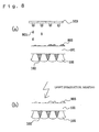
- a volume-type phase device composition 801 is discharged onto the back side of the surface of the light-transmissive substrate 101 where the light-absorption-material pattern 102 and the lens members 105 have already been formed, thereby forming volume-type phase device precursors 802.
- the volume-type phase device precursors 802 are formed of a material having high light transmittance that is substantially flat over the entire visible region, and have a random form and arrangement distribution, which are determined in accordance with the extent to which the coherence of image light is reduced. Such a form and arrangement distribution are provided by randomly changing the liquid amount of the volume-type phase device composition 801 discharged from the piezo jet recording head 103 or by randomly changing the scanning direction and scanning amount of the piezo jet recording head 103.
- the volume-type phase device 803 is provided with more preferable characteristics by, for example, hardening the volume-type phase device precursors 802 by light irradiation, heating, or the like.
- the volume-type phase device 803 on the back side of the surface of the light-transmissive substrate 101 where the lens members 105 are formed, the coherence of image light can be reduced, so that it is possible to enjoy observing a high-quality image having few speckles.
- the lens member compositions or the volume-type phase device composition have been described by referring to optically transparent materials which can be discharged by the piezo jet recording head as an example, it is possible to mix very small particles having light diffusing property in order to further increase the light diffusion action of each lens member.
- very small particles are glass beads, styrene beads, and acrylic beads, which have average particle diameters on the order of a few microns to 20 microns.
- the types of very small particles are not limited to these examples.
- the above-described lens member compositions are applicable to any one of the first to fourth embodiments, and are effective structural materials for adjusting the viewing angle of the transmissive screen.
- the piezo jet recording head has been referred to as the head member which discharges drops of, for example, lens compositions
- other inkjet recording heads having similar functions may be used.
- a typical example is a bubble jet recording head.
- each lens member has been described as having a rectangular form, it may have a circular form, an elliptical form, or an indeterminate form.
- the light-absorption-material patterns have been described as having tapered forms in cross section, they may have rectangular parallelepiped forms or curved forms in cross section.
- very small droplets of lens compositions are discharged onto and land on the light-transmissive substrate.
- the lens members or precursors thereof are formed. This makes it possible to realize at a low cost a bright transmissive screen which has high contrast and which can display a high-quality image having reduced moiré and few speckles.
Landscapes
- Physics & Mathematics (AREA)
- General Physics & Mathematics (AREA)
- Optics & Photonics (AREA)
- Overhead Projectors And Projection Screens (AREA)
Abstract
Description
- Fig. 1
- illustrates the steps of a first embodiment of a method of producing a transmissive screen in accordance with the present invention.
- Fig. 2
- is a plan view and a sectional view of the structural elements used in the first embodiment.
- Fig. 3
- illustrates the light distribution function of a lens member used in the first embodiment.
- Fig. 4
- illustrates the steps of a second embodiment of a method of producing a transmissive screen in accordance with the present invention.
- Fig. 5
- illustrates the steps of a third embodiment of a method of producing a transmissive screen in accordance with the present invention.
- Fig. 6
- illustrates a gap between adjacent landing target locations and the planar form of a lens member to be formed in the third embodiment.
- Fig. 7
- illustrates a gap between some other adjacent landing target locations and the planar form of the lens member to be formed in the third embodiment.
- Fig. 8
- illustrates the steps of a fourth embodiment of a method of producing a transmissive screen in accordance with the present invention.
- Fig. 9
- is a structural view of a lenticular lens sheet.
- Fig. 10
- is a structural view of a planar lens.
- Fig. 11
- illustrates the light distribution of a transmissive screen.
Claims (25)
- A method of producing a transmissive screen having a structure including light-absorption-material patterns that are formed at locations corresponding to locations of lens members, which are provided side by side on a light-transmissive substrate, and to locations of boundary portions between the corresponding lens members, the method comprising the step of forming at least one of the lens members and precursors of the lens members by causing drops of lens compositions to be discharged and to land near a light-transmission area on a surface of the light-transmissive substrate.
- The method of producing a transmissive screen according to Claim 1, wherein means for causing the very small drops of the lens compositions to be discharged and to land is an inkjet recording head.
- The method of producing a transmissive screen according to Claim 2, wherein the inkjet recording head is a piezo jet recording head.
- The method of producing a transmissive screen according to Claim 1, wherein the surface form of each of the lens members is restricted by adjusting the surface tension and viscosity of each of the lens compositions, and the wettability of each of the lens compositions and a surface which each of the lens compositions contacts.
- The method of producing a transmissive screen according to Claim 1, comprising the step of forming the light-absorption-material patterns into the shape of a bank on a surface of the light-transmissive substrate prior to forming at least one of the lens members and the precursors of the lens members by causing the very small drops of the lens compositions to be discharged and to land near a light-transmission portion of the bank-shaped light-absorption-material patterns.
- The method of producing a transmissive screen according to Claim 1, wherein the surface of the light-transmissive substrate on which the light-absorption-material patterns are formed is different from the surface where the lens members are formed.
- The method of producing a transmissive screen according to any one of Claims 1 to 6, wherein the light-absorption-material patterns or the precursors thereof are formed by causing drops of light-absorption-material pattern compositions to be discharged and to land.
- The method of producing a transmissive screen according to Claim 7, wherein means for causing the drops of the light-absorption-material pattern compositions to be discharged and to land is an inkjet recording head.
- The method of producing a transmissive screen according to Claim 8, wherein the inkjet recording head is a piezo jet recording head.
- The method of producing a transmissive screen according to any one of Claims 1 to 9, comprising the step of restricting a planar form of each of the lens members on the surface of the light-transmissive substrate situated at the side where the lens members are formed prior to forming at least one of the lens members and the precursors of the lens members, with the restricting operation being at least one of a chemical operation and a restricted form formation operation, which restrict spreading of the lens member compositions on the transparent substrate.
- The method of producing a transmissive screen according to Claim 10, wherein the step of restricting the planar form of each of the lens members is the same as the step of forming the light-absorption-material patterns.
- The method of producing a transmissive screen according to any one of Claims 1 to 11, wherein adjacent lens members are formed of different lens member compositions.
- The method of producing a transmissive screen according to Claim 12, wherein the different lens member compositions are adjusted so as to only slightly mix with each other.
- A transmissive screen produced by the method of producing a transmissive screen of any one of Claims 1 to 13.
- The transmissive screen according to Claim 14, wherein spectral characteristics of the light-transmissive substrate, each of the lens members, and each of the light-absorption-material patterns are substantially flat in the visible region.
- The transmissive screen according to Claim 14, wherein the form of the bottom side of each of the lens members is substantially rectangular.
- The transmissive screen according to Claim 14, wherein, when the radius of curvature of each of the lens members in a horizontal direction of the transmissive screen is RH and the radius of curvature of each of the lens members in a vertical direction of the transmissive screen is RV, with RH < RV.
- The transmissive screen according to Claim 17, wherein, when the width of each of the lens members in a horizontal direction thereof is WH, and the width of each of the lens members, which is to be formed, in a vertical direction thereof is WV, with WH < WV.
- The transmissive screen according to Claim 14, wherein the distances between adjacent landing target locations of the lens compositions are not uniform in a plane of the transmissive screen.
- The transmissive screen according to Claim 19, wherein the distances between the adjacent landing target locations of the lens compositions in a horizontal direction and those in a vertical direction are different.
- The transmissive screen according to Claim 20, wherein, when the distances between the adjacent landing target locations of the lens compositions in the horizontal direction are PH and those in the vertical direction are PV, PH > PV.
- The transmissive screen according to Claim 21, wherein, when the diameter of the single lens member is SP, the distances between the adjacent landing target locations of the lens compositions are such that PH > SP > PV.
- A method of producing a transmissive screen having a structure including light-absorption-material patterns that are formed on locations corresponding to locations of lens members, which are provided side by side on a light-transmissive substrate, and to locations of boundary portions between the corresponding lens members, the method comprising the step of forming at least one of volume-type phase devices and precursors of volume-type phase devices by causing drops of volume-type phase device compositions to be discharged and to land, with the volume-type phase devices having random phase distributions being provided side by side on at least one of a surface of the light-transmissive substrate where the lens members are formed and the back side of the surface.
- The method of producing a transmissive screen according to Claim 23, wherein means for causing the very small drops of the volume-type phase device compositions to be discharged and to land is an inkjet recording head.
- The method of producing a transmissive screen according to Claim 24, wherein the inkjet recording head is a piezo jet recording head.
Priority Applications (1)
| Application Number | Priority Date | Filing Date | Title |
|---|---|---|---|
| EP05026718A EP1672424A1 (en) | 2000-07-03 | 2001-07-03 | Method of producing a transmissive screen |
Applications Claiming Priority (3)
| Application Number | Priority Date | Filing Date | Title |
|---|---|---|---|
| JP2000201273 | 2000-07-03 | ||
| JP2000201273 | 2000-07-03 | ||
| PCT/JP2001/005774 WO2002003136A1 (en) | 2000-07-03 | 2001-07-03 | Method for manufacturing transmission screen and transmission screen |
Related Child Applications (1)
| Application Number | Title | Priority Date | Filing Date |
|---|---|---|---|
| EP05026718A Division EP1672424A1 (en) | 2000-07-03 | 2001-07-03 | Method of producing a transmissive screen |
Publications (3)
| Publication Number | Publication Date |
|---|---|
| EP1217426A1 true EP1217426A1 (en) | 2002-06-26 |
| EP1217426A4 EP1217426A4 (en) | 2003-07-16 |
| EP1217426B1 EP1217426B1 (en) | 2007-05-16 |
Family
ID=18698996
Family Applications (2)
| Application Number | Title | Priority Date | Filing Date |
|---|---|---|---|
| EP05026718A Withdrawn EP1672424A1 (en) | 2000-07-03 | 2001-07-03 | Method of producing a transmissive screen |
| EP01945808A Expired - Lifetime EP1217426B1 (en) | 2000-07-03 | 2001-07-03 | Method for manufacturing transmission screen and transmission screen |
Family Applications Before (1)
| Application Number | Title | Priority Date | Filing Date |
|---|---|---|---|
| EP05026718A Withdrawn EP1672424A1 (en) | 2000-07-03 | 2001-07-03 | Method of producing a transmissive screen |
Country Status (6)
| Country | Link |
|---|---|
| US (2) | US6621637B2 (en) |
| EP (2) | EP1672424A1 (en) |
| KR (1) | KR100521731B1 (en) |
| CN (1) | CN1203367C (en) |
| DE (1) | DE60128441T2 (en) |
| WO (1) | WO2002003136A1 (en) |
Cited By (8)
| Publication number | Priority date | Publication date | Assignee | Title |
|---|---|---|---|---|
| EP1729172A1 (en) * | 2005-05-30 | 2006-12-06 | Miraial Co., Ltd. | Rear projection type screen |
| CN100552983C (en) * | 2006-07-18 | 2009-10-21 | 财团法人工业技术研究院 | Microlens module of photoelectric component and manufacturing method thereof |
| US7884898B2 (en) | 2005-11-30 | 2011-02-08 | Hitachi Maxwell, Ltd. | Optical sheet for backlight, backlight, and display device |
| WO2014143234A1 (en) * | 2013-03-14 | 2014-09-18 | Integrated Plasmonics Corporation | Self-aligned spatial filter |
| US9404797B2 (en) | 2012-12-07 | 2016-08-02 | Integrated Plasmonics Corporation | Plasmonic spectroscopic sensor and cuvette therefor |
| US9976963B2 (en) | 2012-12-21 | 2018-05-22 | Integrated Plasmonics Corporation | Microcuvette cartridge |
| US9995623B2 (en) | 2013-03-14 | 2018-06-12 | Integrated Plasmonics Corporation | Ambient light assisted spectroscopy |
| US10481089B2 (en) | 2013-03-12 | 2019-11-19 | Integrated Plasmonics Corporation | Optical detection system with tilted sensor |
Families Citing this family (31)
| Publication number | Priority date | Publication date | Assignee | Title |
|---|---|---|---|---|
| US6967779B2 (en) * | 1998-04-15 | 2005-11-22 | Bright View Technologies, Inc. | Micro-lens array with precisely aligned aperture mask and methods of producing same |
| AU7899600A (en) * | 1999-10-18 | 2001-04-30 | Bolin Sun | Large sized rear projection screen |
| FR2836242B1 (en) * | 2002-02-18 | 2004-04-30 | Synelec Telecom Multimedia | PROCESS FOR MANUFACTURING A PROJECTION SCREEN |
| CA2481647A1 (en) * | 2002-04-12 | 2003-10-23 | Duke University | Projection screen apparatus |
| KR100570973B1 (en) * | 2003-05-02 | 2006-04-13 | 삼성에스디아이 주식회사 | Display device having a light blocking substrate and method of manufacturing the same |
| WO2004109239A2 (en) | 2003-06-05 | 2004-12-16 | Cidra Corporation | Apparatus for measuring velocity and flow rate of a fluid having a non-negligible axial mach number using an array of sensors |
| US8031253B2 (en) * | 2003-06-24 | 2011-10-04 | Omnivision International Holding, Ltd. | Image sensor having micro-lens array separated with ridge structures and method of making |
| JP4241259B2 (en) * | 2003-08-06 | 2009-03-18 | セイコーエプソン株式会社 | Microlens manufacturing method |
| KR100608101B1 (en) * | 2004-03-23 | 2006-08-02 | 미래산업 주식회사 | Test handler and picking device of USB memory device |
| JPWO2005107243A1 (en) * | 2004-04-28 | 2008-03-21 | 松下電器産業株式会社 | Imaging device and method for manufacturing microlens array |
| CN100489652C (en) * | 2004-05-15 | 2009-05-20 | 鸿富锦精密工业(深圳)有限公司 | Screen of display |
| US7012754B2 (en) * | 2004-06-02 | 2006-03-14 | Micron Technology, Inc. | Apparatus and method for manufacturing tilted microlenses |
| US7280278B2 (en) * | 2004-06-02 | 2007-10-09 | Micron Technology, Inc. | Apparatus and method for manufacturing positive or negative microlenses |
| JP4340199B2 (en) * | 2004-07-09 | 2009-10-07 | セイコーエプソン株式会社 | Method for manufacturing organic electroluminescence device |
| KR100636349B1 (en) * | 2004-09-24 | 2006-10-19 | 엘지전자 주식회사 | Microlens array sheet and its manufacturing method |
| DE602005022218D1 (en) * | 2004-12-01 | 2010-08-19 | Fujifilm Corp | Structure for increasing the repulsion effect and manufacturing method thereof, liquid ejection head and manufacturing method thereof, and stain resistant film |
| CN101405637A (en) * | 2005-06-29 | 2009-04-08 | 瑞弗莱克塞特公司 | Collimating microlens array |
| JP4948957B2 (en) * | 2006-10-02 | 2012-06-06 | 株式会社 日立ディスプレイズ | Liquid crystal display |
| US7508589B2 (en) * | 2007-02-01 | 2009-03-24 | Real D | Soft aperture correction for lenticular screens |
| US7808708B2 (en) * | 2007-02-01 | 2010-10-05 | Reald Inc. | Aperture correction for lenticular screens |
| JP2010224200A (en) * | 2009-03-24 | 2010-10-07 | Fujifilm Corp | Lenticular print forming method |
| SG178391A1 (en) | 2009-08-13 | 2012-04-27 | Fujifilm Corp | Wafer level, lens, production method of wafer level lens, and imaging unit |
| JP2011081352A (en) * | 2009-09-09 | 2011-04-21 | Fujifilm Corp | Method of manufacturing wafer level lens, wafer level lens and imaging unit |
| CN102147511B (en) * | 2010-02-10 | 2014-09-24 | 新科实业有限公司 | Method for manufacturing polymer micro lens and collimator having the same |
| WO2011155409A1 (en) * | 2010-06-07 | 2011-12-15 | 新日鐵化学株式会社 | Lenticular lens sheet and process for production thereof, and optical element |
| KR20130069712A (en) * | 2010-06-07 | 2013-06-26 | 신닛테츠 수미킨 가가쿠 가부시키가이샤 | Method for producing lenticular lens, lenticular lens, optical element and three-dimensional display device |
| TWI413585B (en) * | 2010-10-13 | 2013-11-01 | Univ Nat Kaohsiung Applied Sci | Method of manufacturing microelements using inkjet technology |
| JP2013178469A (en) * | 2012-02-03 | 2013-09-09 | Nlt Technologies Ltd | Optical element |
| US9266352B2 (en) * | 2013-08-23 | 2016-02-23 | Xerox Corporation | System and method for lenticular image printing and print media |
| CN107479315A (en) * | 2016-06-08 | 2017-12-15 | 深圳市光峰光电技术有限公司 | A kind of movie theatre viewing system |
| CN107128069B (en) * | 2017-04-28 | 2019-07-02 | 京东方科技集团股份有限公司 | Method for regulating inkjet printing device, inkjet printing method, device and system thereof |
Family Cites Families (14)
| Publication number | Priority date | Publication date | Assignee | Title |
|---|---|---|---|---|
| US1942841A (en) * | 1931-01-19 | 1934-01-09 | Shimizu Takeo | Daylight screen |
| US2378252A (en) | 1942-06-30 | 1945-06-12 | Eastman Kodak Co | Projection screen |
| US3552822A (en) | 1968-06-07 | 1971-01-05 | Gerald Altman | Rear projection screen |
| JP2513508Y2 (en) | 1989-08-04 | 1996-10-09 | 株式会社キクチ科学研究所 | Projection screen |
| JP2825887B2 (en) * | 1989-12-12 | 1998-11-18 | 大日本印刷株式会社 | Transmission screen and manufacturing method thereof |
| US5563738A (en) * | 1993-09-03 | 1996-10-08 | Jenmar Visual Systems | Light transmitting and dispersing filter having low reflectance |
| JP3155717B2 (en) | 1996-10-24 | 2001-04-16 | 日本板硝子株式会社 | Laser processing method for micro lens |
| GB9800668D0 (en) * | 1998-01-13 | 1998-03-11 | Nashua Corp | Enhanced microlens screens |
| JP4193225B2 (en) | 1998-03-16 | 2008-12-10 | 凸版印刷株式会社 | Lenticular sheet and manufacturing method thereof |
| JP3965541B2 (en) | 1998-08-27 | 2007-08-29 | セイコーエプソン株式会社 | Manufacturing method of microlens array |
| US6297911B1 (en) | 1998-08-27 | 2001-10-02 | Seiko Epson Corporation | Micro lens array, method of fabricating the same, and display device |
| JP2000108216A (en) * | 1998-10-02 | 2000-04-18 | Canon Inc | Manufacturing method of micro lens array |
| JP3687366B2 (en) * | 1998-10-23 | 2005-08-24 | セイコーエプソン株式会社 | Optical substrate, manufacturing method thereof, and display device |
| JP3038329B1 (en) | 1998-11-24 | 2000-05-08 | 日清紡績株式会社 | Method of manufacturing lenticular lens and method of manufacturing three-dimensional or variable printed matter using lens by the method |
-
2001
- 2001-07-03 EP EP05026718A patent/EP1672424A1/en not_active Withdrawn
- 2001-07-03 DE DE60128441T patent/DE60128441T2/en not_active Expired - Fee Related
- 2001-07-03 WO PCT/JP2001/005774 patent/WO2002003136A1/en not_active Ceased
- 2001-07-03 KR KR10-2002-7002845A patent/KR100521731B1/en not_active Expired - Fee Related
- 2001-07-03 CN CNB018026834A patent/CN1203367C/en not_active Expired - Fee Related
- 2001-07-03 US US10/069,756 patent/US6621637B2/en not_active Expired - Fee Related
- 2001-07-03 EP EP01945808A patent/EP1217426B1/en not_active Expired - Lifetime
-
2003
- 2003-07-16 US US10/619,455 patent/US6839178B2/en not_active Expired - Fee Related
Cited By (10)
| Publication number | Priority date | Publication date | Assignee | Title |
|---|---|---|---|---|
| EP1729172A1 (en) * | 2005-05-30 | 2006-12-06 | Miraial Co., Ltd. | Rear projection type screen |
| US7884898B2 (en) | 2005-11-30 | 2011-02-08 | Hitachi Maxwell, Ltd. | Optical sheet for backlight, backlight, and display device |
| CN100552983C (en) * | 2006-07-18 | 2009-10-21 | 财团法人工业技术研究院 | Microlens module of photoelectric component and manufacturing method thereof |
| US9404797B2 (en) | 2012-12-07 | 2016-08-02 | Integrated Plasmonics Corporation | Plasmonic spectroscopic sensor and cuvette therefor |
| US9976963B2 (en) | 2012-12-21 | 2018-05-22 | Integrated Plasmonics Corporation | Microcuvette cartridge |
| US10481089B2 (en) | 2013-03-12 | 2019-11-19 | Integrated Plasmonics Corporation | Optical detection system with tilted sensor |
| WO2014143234A1 (en) * | 2013-03-14 | 2014-09-18 | Integrated Plasmonics Corporation | Self-aligned spatial filter |
| US9784986B2 (en) | 2013-03-14 | 2017-10-10 | Integrated Plasmonics Corporation | Self-aligned spatial filter |
| US9995623B2 (en) | 2013-03-14 | 2018-06-12 | Integrated Plasmonics Corporation | Ambient light assisted spectroscopy |
| US10241347B2 (en) | 2013-03-14 | 2019-03-26 | Integrated Plasmonics Corporation | Self-aligned spatial filter |
Also Published As
| Publication number | Publication date |
|---|---|
| US6621637B2 (en) | 2003-09-16 |
| WO2002003136A1 (en) | 2002-01-10 |
| CN1388917A (en) | 2003-01-01 |
| US6839178B2 (en) | 2005-01-04 |
| EP1217426A4 (en) | 2003-07-16 |
| EP1217426B1 (en) | 2007-05-16 |
| CN1203367C (en) | 2005-05-25 |
| KR100521731B1 (en) | 2005-10-17 |
| US20040012857A1 (en) | 2004-01-22 |
| DE60128441D1 (en) | 2007-06-28 |
| US20020149709A1 (en) | 2002-10-17 |
| DE60128441T2 (en) | 2008-02-14 |
| EP1672424A1 (en) | 2006-06-21 |
| KR20020029397A (en) | 2002-04-18 |
Similar Documents
| Publication | Publication Date | Title |
|---|---|---|
| US6621637B2 (en) | Method for manufacturing transmission screen and transmission screen | |
| KR100819411B1 (en) | Method of manufacturing optical sheet, optical sheet, backlight unit, display device, and electronic apparatus | |
| CN110865509B (en) | Projection screen and manufacturing method thereof | |
| US7808706B2 (en) | Light management films for displays | |
| CN105204282B (en) | Projection screen and manufacturing method thereof | |
| KR20080105026A (en) | Screens for Optical Sheets, Image Display Devices and Image Projection Devices | |
| EP1899759A2 (en) | Collimating microlens array | |
| JP2006526811A (en) | Microlens array-based high-resolution, low-image artifact transmissive screen | |
| TW200821631A (en) | Condensing sheet and method for preparing thereof | |
| US7332852B2 (en) | One-way transparent optical system having light absorption elements and light refracting structures | |
| JP2012163785A (en) | Optical sheet, light source unit, and liquid crystal display | |
| JP2009063849A (en) | Light diffusing screen, manufacturing method thereof, and rear projection display device | |
| JP2006030596A (en) | Lenticular lens sheet, manufacturing method thereof, transmissive screen, and rear projection display device | |
| JP2008262208A (en) | Light diffusion sheet and projection screen | |
| KR20190010888A (en) | Optical film and lighting apparatus using the same | |
| JP5228171B2 (en) | Optical element | |
| CN113075853B (en) | Projection film and projection apparatus | |
| WO2011162165A1 (en) | Method for manufacturing light-diffusing film, light-diffusing film manufactured by the method, and display device provided with the light-diffusing film | |
| JP2007003983A (en) | Manufacturing method of optical sheet, optical sheet, backlight unit, display device, electronic device | |
| CN222146266U (en) | Peep-proof film and display panel thereof | |
| JP2012022314A (en) | Light reflection sheet and light source unit | |
| JPWO2002003136A1 (en) | Manufacturing method of transmission screen and transmission screen | |
| JP4476188B2 (en) | Optical device, light absorption method, and light absorption layer manufacturing method | |
| KR20170089177A (en) | Optical film and lighting apparatus using the same | |
| JP2005331536A (en) | Manufacturing method of lens sheet having light shielding band |
Legal Events
| Date | Code | Title | Description |
|---|---|---|---|
| PUAI | Public reference made under article 153(3) epc to a published international application that has entered the european phase |
Free format text: ORIGINAL CODE: 0009012 |
|
| 17P | Request for examination filed |
Effective date: 20020403 |
|
| AK | Designated contracting states |
Kind code of ref document: A1 Designated state(s): AT BE CH CY DE DK ES FI FR GB GR IE IT LI LU MC NL PT SE TR |
|
| AX | Request for extension of the european patent |
Free format text: AL;LT;LV;MK;RO;SI |
|
| A4 | Supplementary search report drawn up and despatched |
Effective date: 20030604 |
|
| RBV | Designated contracting states (corrected) |
Designated state(s): AT BE CH DE FR GB LI |
|
| GRAP | Despatch of communication of intention to grant a patent |
Free format text: ORIGINAL CODE: EPIDOSNIGR1 |
|
| RBV | Designated contracting states (corrected) |
Designated state(s): DE FR GB |
|
| GRAS | Grant fee paid |
Free format text: ORIGINAL CODE: EPIDOSNIGR3 |
|
| GRAA | (expected) grant |
Free format text: ORIGINAL CODE: 0009210 |
|
| AK | Designated contracting states |
Kind code of ref document: B1 Designated state(s): DE FR GB |
|
| REG | Reference to a national code |
Ref country code: GB Ref legal event code: FG4D |
|
| REF | Corresponds to: |
Ref document number: 60128441 Country of ref document: DE Date of ref document: 20070628 Kind code of ref document: P |
|
| ET | Fr: translation filed | ||
| PLBE | No opposition filed within time limit |
Free format text: ORIGINAL CODE: 0009261 |
|
| STAA | Information on the status of an ep patent application or granted ep patent |
Free format text: STATUS: NO OPPOSITION FILED WITHIN TIME LIMIT |
|
| 26N | No opposition filed |
Effective date: 20080219 |
|
| PGFP | Annual fee paid to national office [announced via postgrant information from national office to epo] |
Ref country code: FR Payment date: 20090710 Year of fee payment: 9 |
|
| PGFP | Annual fee paid to national office [announced via postgrant information from national office to epo] |
Ref country code: DE Payment date: 20090626 Year of fee payment: 9 Ref country code: GB Payment date: 20090701 Year of fee payment: 9 |
|
| GBPC | Gb: european patent ceased through non-payment of renewal fee |
Effective date: 20100703 |
|
| REG | Reference to a national code |
Ref country code: FR Ref legal event code: ST Effective date: 20110331 |
|
| PG25 | Lapsed in a contracting state [announced via postgrant information from national office to epo] |
Ref country code: DE Free format text: LAPSE BECAUSE OF NON-PAYMENT OF DUE FEES Effective date: 20110201 |
|
| REG | Reference to a national code |
Ref country code: DE Ref legal event code: R119 Ref document number: 60128441 Country of ref document: DE Effective date: 20110201 |
|
| PG25 | Lapsed in a contracting state [announced via postgrant information from national office to epo] |
Ref country code: FR Free format text: LAPSE BECAUSE OF NON-PAYMENT OF DUE FEES Effective date: 20100802 |
|
| PG25 | Lapsed in a contracting state [announced via postgrant information from national office to epo] |
Ref country code: GB Free format text: LAPSE BECAUSE OF NON-PAYMENT OF DUE FEES Effective date: 20100703 |