EP1216420B1 - Integrated test cell - Google Patents
Integrated test cell Download PDFInfo
- Publication number
- EP1216420B1 EP1216420B1 EP00970501A EP00970501A EP1216420B1 EP 1216420 B1 EP1216420 B1 EP 1216420B1 EP 00970501 A EP00970501 A EP 00970501A EP 00970501 A EP00970501 A EP 00970501A EP 1216420 B1 EP1216420 B1 EP 1216420B1
- Authority
- EP
- European Patent Office
- Prior art keywords
- tester
- handling apparatus
- semiconductor
- frame
- probe ring
- Prior art date
- Legal status (The legal status is an assumption and is not a legal conclusion. Google has not performed a legal analysis and makes no representation as to the accuracy of the status listed.)
- Expired - Lifetime
Links
- 238000012360 testing method Methods 0.000 title claims abstract description 36
- 239000004065 semiconductor Substances 0.000 claims abstract description 36
- 238000003032 molecular docking Methods 0.000 claims abstract description 14
- 239000000523 sample Substances 0.000 claims description 27
- 230000000712 assembly Effects 0.000 claims description 7
- 238000000429 assembly Methods 0.000 claims description 7
- 230000007246 mechanism Effects 0.000 claims description 5
- 230000006835 compression Effects 0.000 claims description 3
- 238000007906 compression Methods 0.000 claims description 3
- 230000008901 benefit Effects 0.000 description 6
- 238000001816 cooling Methods 0.000 description 4
- 238000000034 method Methods 0.000 description 4
- 235000012431 wafers Nutrition 0.000 description 4
- 229910000831 Steel Inorganic materials 0.000 description 3
- 238000004519 manufacturing process Methods 0.000 description 3
- 239000010959 steel Substances 0.000 description 3
- 230000008878 coupling Effects 0.000 description 2
- 238000010168 coupling process Methods 0.000 description 2
- 238000005859 coupling reaction Methods 0.000 description 2
- 230000009467 reduction Effects 0.000 description 2
- 230000009286 beneficial effect Effects 0.000 description 1
- 230000003749 cleanliness Effects 0.000 description 1
- 238000010276 construction Methods 0.000 description 1
- 238000006073 displacement reaction Methods 0.000 description 1
- 239000000428 dust Substances 0.000 description 1
- 230000000694 effects Effects 0.000 description 1
- 230000008713 feedback mechanism Effects 0.000 description 1
- 238000009434 installation Methods 0.000 description 1
- 210000003141 lower extremity Anatomy 0.000 description 1
- 238000012423 maintenance Methods 0.000 description 1
- 239000002245 particle Substances 0.000 description 1
- 230000003449 preventive effect Effects 0.000 description 1
- 230000008569 process Effects 0.000 description 1
- 230000008439 repair process Effects 0.000 description 1
- 230000000007 visual effect Effects 0.000 description 1
- XLYOFNOQVPJJNP-UHFFFAOYSA-N water Substances O XLYOFNOQVPJJNP-UHFFFAOYSA-N 0.000 description 1
Images

Classifications
-
- G—PHYSICS
- G01—MEASURING; TESTING
- G01R—MEASURING ELECTRIC VARIABLES; MEASURING MAGNETIC VARIABLES
- G01R31/00—Arrangements for testing electric properties; Arrangements for locating electric faults; Arrangements for electrical testing characterised by what is being tested not provided for elsewhere
- G01R31/28—Testing of electronic circuits, e.g. by signal tracer
- G01R31/2851—Testing of integrated circuits [IC]
- G01R31/2886—Features relating to contacting the IC under test, e.g. probe heads; chucks
- G01R31/2887—Features relating to contacting the IC under test, e.g. probe heads; chucks involving moving the probe head or the IC under test; docking stations
Definitions
- the invention relates generally to automatic test equipment for testing semiconductor devices, and more particularly an integrated automatic test system having a substantially reduced footprint for testing semiconductor devices.
- the equipment generally drives waveforms to and detects outputs from one or more devices-under-test (DUT). The detected outputs are then compared to expected values to determine whether the device functioned properly.
- DUT devices-under-test
- a critical concern for semiconductor manufacturers is how to maximize use of the limited floor space available for test.
- stringent cleanliness requirements are imposed while testing semiconductor devices to minimize the possibility of failures due to dust or debris.
- the automatic test equipment resides in sophisticated clean rooms that minimize the size and number of particles according to particular applications. Because of the cost necessary to operate and maintain clean rooms, maximizing clean room floor space is essential to minimizing manufacturing costs.
- One type of conventional semiconductor tester generally includes a mainframe computer, or test controller, and a testhead coupled to the controller via a relatively large cable bundle.
- the testhead typically weighs several hundred kilograms and houses a plurality of channel cards that include complex circuitry for coupling to the semiconductor devices-under-test (DUTs).
- the testhead is fixed to a manipulator that moves and adjusts the testhead into a variety of positions as needed.
- Efficient semiconductor device testing generally requires an apparatus to move and quickly connect the device-under-test (DUT) to the tester.
- DUT device-under-test
- a machine called a prober is employed.
- a handler is used. These units precisely position the semiconductor devices so that they make contact with the outputs of the tester. Probers, handlers and other devices for positioning a DUT relative to the testhead are called generically "handling apparatus.”
- a semiconductor tester positions a mainframe/testhead unit vertically on top of a prober or handler.
- An example of this type of tester is found in the Teradyne Model J750 Tester, manufactured by Teradyne Inc., Boston, Massachusetts. This construction dramatically reduces the tester footprint by making advantageous use of the vertical dimensions of the clean room. As a result, more testers are able to fit within a given horizontal clean room space.
- the prober or handler generally supports the mainframe/testhead unit.
- a manipulator is still often required for servicing purposes, such as the initial installation of the unit or temporary removal of the mainframe/testhead unit from the handler or prober. Consequently, in order to plan for occasional servicing, space often must be made available in the clean room for the ingress and egress of the manipulator. The space set aside thus displaces potential floor room area for more testers and greater throughput.
- the integrated test cell of the present invention provides the capability of servicing a semiconductor tester without undocking from a handling device such as a prober or handler. As a result, the use of a manipulator is unnecessary, thereby dramatically reducing costs. This also contributes to a significant reduction in the mean-time-to-repair (MTTR) parameter of the tester. Moreover, the vertical nature of the test cell presents a substantially reduced footprint, enabling the maximization of available clean room floor space.
- MTTR mean-time-to-repair
- the invention in one form comprises a semiconductor tester that is adapted for testing semiconductor devices disposed on a handling apparatus.
- the semiconductor tester includes a tester housing defining a self-supporting frame and formed with an externally accessible opening adapted for receiving the handling apparatus.
- a test controller is disposed within the housing and carried by the frame.
- Pin electronics including tester circuitry are responsive to the test controller and proximately coupled thereto and mounted to the frame.
- a docking apparatus is disposed above the opening and is adapted to couple the tester circuitry to the handling apparatus.
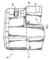
- a semiconductor tester according to one embodiment of the present invention and generally designated 10, provides substantial advantages in manufacturing efficiency by minimizing the tester footprint associated with the horizontal dimensions of the tester system.
- the footprint is minimized by utilizing a self-supporting frame 12 formed with an opening 52 adapted to slidably receive a handling apparatus 54 ( Figure 4).
- Pin electronics 39 ( Figure 2) are mounted in the frame along with a docking apparatus 80 ( Figure 5).
- the docking apparatus provides convenient serviceability of the docked handling apparatus without the use of a manipulator, thereby allowing relatively high tester system density within a given cleanroom, and correspondingly reducing manufacturing costs.
- the frame 12 is formed with respective oppositely disposed first and second base supports 14 and 28 for carrying an electronics platform 30.
- the entire frame structure is constructed of steel and projects vertically to define a relatively small horizontal footprint.
- the first base support 14 is formed with an upstanding rectangular cross-section and includes a plurality of open compartments for mounting a test controller or central processing unit (CPU) 16, a cooling distribution unit (CDU) 18, and a power distribution unit (PDU) 20.
- a pair of spaced apart levelers 22 and 24 provide an adjustable leveling capability at the fore section of the first base support while the aft portion includes a convenient water and power access port 26.
- the second base support 28 projects vertically in substantially parallel relationship with the first support. Formed relatively narrow in rectangular cross-section, the second base support includes at its lower extremity a pair of oppositely disposed casters 29 (only one caster shown).
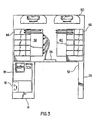
- the electronics platform 30 is formed integral with the base supports 14 and 28 and is disposed horizontally thereacross.
- the platform includes a network of welded bars cooperating to form a lateral rectangular structure and defining respective first and second cavities 32 and 34.
- the cavities are positioned above and on opposing sides of a circular-shaped probe ring 36 ( Figure 3) and adapted for mounting respective first and second cardcage assemblies 38 and 40.
- the cardcage assemblies house the tester pin electronics 39 for testing semiconductor devices (not shown).
- the platform includes an aft section formed with a vertically extending rack framework 42 for nesting respective stacks of power supplies 44 and 46 ( Figure 3).
- a cooling system support structure 48 formed to carry a plurality of fans 50 and heat exchangers 51.
- the fans and heat exchangers form a portion of a sealed cooling system more fully described in pending U.S. Patent No. 6,208,510, entitled Semiconductor Tester Cooling System", filed July 23, 1999, assigned to the assignee of the present invention, and hereby expressly incorporated herein by reference.
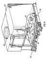
- the first and second base supports 14 and 28 and the electronics platform 30 collectively form a laterally accessible opening 52 adapted to slidably receive the handling apparatus 54 ( Figure 4).
- the handling apparatus 54 is preferably slidably carried by a mobile cart apparatus 60.
- the cart apparatus includes respective fore and aft steel channel supports 62 and 64 disposed in parallel relationship and bounded laterally by a pair of side beams 66 and 68 fixed thereto.
- the side beams and channel supports cooperate to form a rectangular platform.
- a vertically upstanding steel handle 70 is mounted to the fore channel support 62 for effecting maneuverability of the prober/cart assembly with a push/pull force of around twenty-five pounds (1 pound ⁇ 454g).
- a plurality of locking casters 72 provide the necessary selective mobility.
- Conveniently positioned visual indicators cooperate with a feedback mechanism (not shown) for providing a coarse alignment capability for the operator as the unit installs within the frame opening 52.
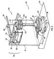
- the docking apparatus 80 is conveniently adapted to align and dock the semiconductor tester 10 to the handling apparatus (not shown).
- the docking apparatus includes the probe ring assembly 36 and a self-alignment mechanism 90 for enabling precise manual alignment of the probe ring with the handling apparatus (not shown) by a single operator.
- the probe ring assembly 36 is formed in a circular shape with modular compartments or cavities (not shown) to provide high density routing of signal channels between the pin electronics of the tester 10 and a parallel array of devices-under-test (not shown) disposed on a prober-supported wafer (not shown).
- a radially projecting handle 82 and a plurality of cam grooves 83 are disposed at the periphery of the ring.
- the probe ring and associated routing circuitry for coupling the pin electronics 39 to the handling apparatus 54 are more fully described in copending U.S. Patent Application Serial Number 09/340,832, entitled “Semiconductor Parallel Tester", filed June 28, 1999, assigned to the assignee of the present invention, and hereby expressly incorporated herein by reference.
- the self-alignment mechanism 90 is carried by respective lateral and longitudinal support members 92 and 94 welded to the frame 12 in close proximity to one of the card cage backplane assemblies 91.
- the alignment mechanism couples to the probe ring 36 through a vertically extending arm that serves as a compression bar 96 during operation.
- the arm is secured to the probe ring by a connector 97 that couples to a pivot 98.
- a multi axis X-Y table 100 is mounted atop the extension arm and comprises respective linear bearings 102 and 104 for horizontally directing the probe ring along the X and Y axes.
- a counterweight assembly 106 couples to the compression bar and includes a counterweight 108 slidable along a guide rail 110 and tethered to the extension arm via a cable 112 that traverses a pair of in-line pulleys 114 and 118 for effecting vertical displacement of the probe ring.
- a preferred handling apparatus 54 is the TEL P8XL Prober, manufactured by Tokyo Electronics, Ltd., of Tokyo, Japan.
- the prober includes a base ring that is formed with a plurality of cam followers 85 for engaging the cam grooves 83. Also provided is an automatic probe card changer (not shown) for compressing the probe ring pogo pins (not shown).
- This machine is known to have a high z-force chuck that can serve a 32-site, high pin count application.
- the prober may share an operator interface 120 ( Figure 1) with the tester 10 to advantageously minimize the number of monitor displays and keyboards for the system operator.
- a preferred handling apparatus 54 comprises the Galileo model Handler, manufactured by Kinetrix, Inc., of Bedford, New Hampshire.
- the handler manipulates standard JEDEC device trays and provides DUT hot and cold soak capability. Additionally, the handler is optimized for moving DUTs in and out of contactor sockets, providing very low jam rates and high throughput.
- the initial set-up of the test system involves installing the prober within the frame opening 52 by engaging the prober with the cart apparatus 60. This involves first positioning the cart apparatus beneath the prober such that the prober leveling feet are carried by the channel supports 62 and 64. The prober is then slid into the frame opening 52 and leveled. Once the prober is coarsely aligned within the opening with respect to the probe ring, the operator can commence the following docking steps to hard-dock the docking apparatus to the prober.
- the operator initiates docking by manually lowering the probe ring 36 onto the base ring.
- the probe ring is able to move fore, aft, and laterally due to the X-Y table 100 at the point of connection to the tester mainframe. This allows for minor misalignments between the prober and tester.
- the probe ring is able to easily move up and down due to the pulleyed counterweight 108.
- one or more semiconductor devices at the wafer level are then tested. This usually involves the application and capture of tester waveforms to and from the device(s) according to processes well known to those skilled in the art.
- the handling apparatus 54 and/or tester 10 may require servicing to, for example access the prober head plate 122 ( Figure 4) for preventive maintenance. Because of the self-supporting nature of the tester frame, no manipulator is required to assist in the undocking procedure to effect the servicing. Rather, an operator merely decouples the probe ring from the prober by releasing the fasteners, and lifting the probe ring via the probe ring handle.
Landscapes
- Engineering & Computer Science (AREA)
- Computer Hardware Design (AREA)
- Microelectronics & Electronic Packaging (AREA)
- General Engineering & Computer Science (AREA)
- Physics & Mathematics (AREA)
- General Physics & Mathematics (AREA)
- Testing Or Measuring Of Semiconductors Or The Like (AREA)
- Testing Of Individual Semiconductor Devices (AREA)
- Tests Of Electronic Circuits (AREA)
- Liquid Developers In Electrophotography (AREA)
- Investigating Or Analysing Biological Materials (AREA)
- Electron Tubes For Measurement (AREA)
Abstract
Description
Claims (6)
- A semiconductor tester (10) adapted for testing semiconductor devices disposed on a handling apparatus (54), said semiconductor tester including:a tester housing defining a self-supporting frame (12) and formed with an externally accessible opening (52), said opening adapted for receiving said handling apparatus;a test controller (16) disposed within said housing and carried by said frame;pin electronics (39) including tester circuitry responsive to said test controller and proximately coupled to said test controller and mounted to said frame; anda docking apparatus (80) disposed above said opening and adapted to couple said tester circuitry to said handling apparatus.
- A semiconductor tester (10) according to claim 1 wherein said docking apparatus (80) includes a probe ring assembly including a probe ring (36) adapted to engage said handling apparatus (54).
- A semiconductor tester (10) according to claim 1 wherein said probe ring assembly includes a self-alignment mechanism (90) adapted for aligning said probe ring (36) with said handling apparatus.
- A semiconductor tester (10) according to claim 3 wherein said self-alignment mechanism (90) includes:a multi-axis table (100);a vertically extending compression bar (96) fixed to said multi-axis table and fastened to said probe ring via a pivot (90) disposed on said ring; anda handle (82) mounted to said probe ring for manually pivoting said probe ring about said pivot.
- A semiconductor tester (10) according to claim 1 wherein:said frame (12) defines a plurality of cardcage assemblies (38, 40); andsaid pin electronics (39) comprise a plurality of channel cards disposed in spaced-apart relationship in said card-cage assemblies.
- A semiconductor tester (10) according to claim 5 wherein:said frame (12) includes respective first and second base supports (14, 28), and said opening (52) is formed intermediate said base supports; andsaid cardcage assemblies (38, 40) comprise a pair of cardcages set in opposing spaced-apart relationship above said opening.
Applications Claiming Priority (3)
| Application Number | Priority Date | Filing Date | Title |
|---|---|---|---|
| US410857 | 1982-08-23 | ||
| US09/410,857 US6310486B1 (en) | 1999-10-01 | 1999-10-01 | Integrated test cell |
| PCT/US2000/026597 WO2001025801A1 (en) | 1999-10-01 | 2000-09-28 | Integrated test cell |
Publications (2)
| Publication Number | Publication Date |
|---|---|
| EP1216420A1 EP1216420A1 (en) | 2002-06-26 |
| EP1216420B1 true EP1216420B1 (en) | 2003-05-21 |
Family
ID=23626525
Family Applications (1)
| Application Number | Title | Priority Date | Filing Date |
|---|---|---|---|
| EP00970501A Expired - Lifetime EP1216420B1 (en) | 1999-10-01 | 2000-09-28 | Integrated test cell |
Country Status (9)
| Country | Link |
|---|---|
| US (1) | US6310486B1 (en) |
| EP (1) | EP1216420B1 (en) |
| JP (1) | JP4800534B2 (en) |
| KR (1) | KR100672824B1 (en) |
| AT (1) | ATE241143T1 (en) |
| DE (1) | DE60002899T2 (en) |
| MY (1) | MY120188A (en) |
| TW (1) | TW479306B (en) |
| WO (1) | WO2001025801A1 (en) |
Families Citing this family (14)
| Publication number | Priority date | Publication date | Assignee | Title |
|---|---|---|---|---|
| DE10102541A1 (en) * | 2001-01-19 | 2002-07-25 | Leica Microsystems | Measuring and analysis apparatus for microscopic observation of semiconductor wafers has electrical control components releasably attached to frame |
| US6756800B2 (en) * | 2002-04-16 | 2004-06-29 | Teradyne, Inc. | Semiconductor test system with easily changed interface unit |
| US6864698B2 (en) * | 2003-03-24 | 2005-03-08 | Teradyne, Inc. | Hybrid cooling system for automatic test equipment |
| US7701232B2 (en) * | 2007-01-23 | 2010-04-20 | Teradyne, Inc. | Rotational positioner and methods for semiconductor wafer test systems |
| JP5277827B2 (en) * | 2008-09-22 | 2013-08-28 | 東京エレクトロン株式会社 | Probe device |
| TWM359791U (en) * | 2008-12-31 | 2009-06-21 | Princeton Technology Corp | Semiconductor device test system |
| GB201015767D0 (en) * | 2010-09-18 | 2010-10-27 | Loveridge Michael J | Suspended attachment rail apparatus |
| CN103196924B (en) * | 2012-01-09 | 2015-03-25 | 京元电子股份有限公司 | docking test system |
| US9726718B2 (en) | 2014-05-30 | 2017-08-08 | Skyworks Solutions, Inc. | Modular test fixture |
| US12174249B2 (en) | 2022-05-06 | 2024-12-24 | Nanya Technology Corporation | Probing device and inspection method using the same |
| US11828797B1 (en) | 2022-05-06 | 2023-11-28 | Nanya Technology Corporation | Probing device |
| TWI817647B (en) * | 2022-05-06 | 2023-10-01 | 南亞科技股份有限公司 | Probing device |
| KR102720145B1 (en) * | 2024-04-08 | 2024-10-21 | 주식회사 에이아이로보틱스 | Slide docking type mobile test handler apparatus |
| CN120722167B (en) * | 2025-07-28 | 2026-02-17 | 深圳市华测半导体设备有限公司 | IC Integrated Circuit Reliability Testing Machine and Testing Methods |
Family Cites Families (25)
| Publication number | Priority date | Publication date | Assignee | Title |
|---|---|---|---|---|
| EP0382264B1 (en) * | 1984-06-29 | 1994-06-15 | Advantest Corporation | IC test equipment |
| JPH065260B2 (en) * | 1986-08-29 | 1994-01-19 | 日立電子エンジニアリング株式会社 | IC handler |
| US4926118A (en) * | 1988-02-22 | 1990-05-15 | Sym-Tek Systems, Inc. | Test station |
| DE3903607A1 (en) * | 1989-02-08 | 1990-08-09 | Leybold Ag | DEVICE FOR CLEANING, CHECKING AND CLASSIFYING WORKPIECES |
| DE4040870A1 (en) | 1990-12-20 | 1992-06-25 | Krautkraemer Gmbh | WHOLE BODY TEST SYSTEM WITH A TEST HEAD SUPPORT IN PARTICULAR DESIGNED AS A ROTOR, THAT IS ADJUSTED ON A HEIGHT-ADJUSTABLE ADJUSTMENT, AND WITH A TEST PIECE MANIPULATOR |
| US5126656A (en) | 1991-05-31 | 1992-06-30 | Ej Systems, Inc. | Burn-in tower |
| US5164661A (en) | 1991-05-31 | 1992-11-17 | Ej Systems, Inc. | Thermal control system for a semi-conductor burn-in |
| US5241870A (en) | 1991-07-22 | 1993-09-07 | Intest Corporation | Test head manipulator |
| JP2873411B2 (en) * | 1991-08-03 | 1999-03-24 | 東京エレクトロン株式会社 | Probe device |
| JP2821046B2 (en) * | 1991-09-05 | 1998-11-05 | 三菱電機エンジニアリング株式会社 | Characteristics inspection equipment for semiconductor devices |
| US5307011A (en) * | 1991-12-04 | 1994-04-26 | Advantest Corporation | Loader and unloader for test handler |
| US5420521A (en) | 1992-10-27 | 1995-05-30 | Ej Systems, Inc. | Burn-in module |
| US5440943A (en) * | 1993-09-15 | 1995-08-15 | Intest Corporation | Electronic test head manipulator |
| US5600258A (en) | 1993-09-15 | 1997-02-04 | Intest Corporation | Method and apparatus for automated docking of a test head to a device handler |
| JPH07147305A (en) * | 1993-11-25 | 1995-06-06 | Tokyo Electron Ltd | Device under test |
| US5506512A (en) * | 1993-11-25 | 1996-04-09 | Tokyo Electron Limited | Transfer apparatus having an elevator and prober using the same |
| TW273635B (en) | 1994-09-01 | 1996-04-01 | Aesop | |
| KR960019641A (en) | 1994-11-24 | 1996-06-17 | 오우라 히로시 | Semiconductor test equipment equipped with a test head connection device |
| JP3869465B2 (en) * | 1995-02-23 | 2007-01-17 | テラダイン・インコーポレーテッド | Manipulator for test head of automatic test equipment |
| US5606262A (en) | 1995-06-07 | 1997-02-25 | Teradyne, Inc. | Manipulator for automatic test equipment test head |
| US6024526A (en) * | 1995-10-20 | 2000-02-15 | Aesop, Inc. | Integrated prober, handler and tester for semiconductor components |
| US5654631A (en) | 1995-11-15 | 1997-08-05 | Xilinx, Inc. | Vacuum lock handler and tester interface for semiconductor devices |
| US6023173A (en) * | 1997-04-30 | 2000-02-08 | Credence Systems Corporation | Manipulator with expanded range of motion |
| US5949002A (en) | 1997-11-12 | 1999-09-07 | Teradyne, Inc. | Manipulator for automatic test equipment with active compliance |
| US6031387A (en) * | 1997-12-02 | 2000-02-29 | Credence Systems Corporation | Semiconductor test system with integrated test head manipulator and device handler |
-
1999
- 1999-10-01 US US09/410,857 patent/US6310486B1/en not_active Expired - Lifetime
-
2000
- 2000-09-28 JP JP2001528710A patent/JP4800534B2/en not_active Expired - Lifetime
- 2000-09-28 DE DE60002899T patent/DE60002899T2/en not_active Expired - Fee Related
- 2000-09-28 MY MYPI20004523A patent/MY120188A/en unknown
- 2000-09-28 EP EP00970501A patent/EP1216420B1/en not_active Expired - Lifetime
- 2000-09-28 AT AT00970501T patent/ATE241143T1/en not_active IP Right Cessation
- 2000-09-28 TW TW089120056A patent/TW479306B/en not_active IP Right Cessation
- 2000-09-28 WO PCT/US2000/026597 patent/WO2001025801A1/en not_active Ceased
- 2000-09-28 KR KR1020027004217A patent/KR100672824B1/en not_active Expired - Lifetime
Also Published As
| Publication number | Publication date |
|---|---|
| ATE241143T1 (en) | 2003-06-15 |
| DE60002899T2 (en) | 2004-05-13 |
| KR100672824B1 (en) | 2007-01-22 |
| DE60002899D1 (en) | 2003-06-26 |
| JP2003511852A (en) | 2003-03-25 |
| JP4800534B2 (en) | 2011-10-26 |
| TW479306B (en) | 2002-03-11 |
| WO2001025801A1 (en) | 2001-04-12 |
| US6310486B1 (en) | 2001-10-30 |
| EP1216420A1 (en) | 2002-06-26 |
| MY120188A (en) | 2005-09-30 |
| KR20020044155A (en) | 2002-06-14 |
Similar Documents
| Publication | Publication Date | Title |
|---|---|---|
| US6310486B1 (en) | Integrated test cell | |
| US7385385B2 (en) | System for testing DUT and tester for use therewith | |
| EP2506021B1 (en) | Test head positioning system and method | |
| US5656942A (en) | Prober and tester with contact interface for integrated circuits-containing wafer held docked in a vertical plane | |
| US7023225B2 (en) | Wafer-mounted micro-probing platform | |
| KR102221204B1 (en) | Manipulator | |
| KR101284407B1 (en) | Carousel device, system and method for electronic circuit tester | |
| US11594435B2 (en) | Apparatus and methods for testing semiconductor devices | |
| US8350584B2 (en) | Test head positioning system and method | |
| KR101474584B1 (en) | Apparatus for attaching load port apparatus | |
| EP1495339B1 (en) | Semiconductor test system with easily changed interface unit | |
| JPH08335614A (en) | Probe system | |
| US6741072B2 (en) | Docking system for connecting a tester to a probe station using an A-type docking configuration | |
| US20250155492A1 (en) | Multi-wafer inspection system | |
| US6717432B2 (en) | Single axis manipulator with controlled compliance | |
| JPH0666365B2 (en) | Probe device | |
| TW202315240A (en) | Electronic device test vehicle and transportation test system | |
| CN115882277A (en) | Electronic device test trolley and transport test system | |
| KR102136544B1 (en) | Wafer prober being capable of easy maintenance | |
| CN224231901U (en) | Flying probe tester | |
| CN219978373U (en) | Probe testing device for chip testing | |
| JPH04290450A (en) | Semiconductor inspection equipment | |
| CN113611644A (en) | Substrate processing system for processing substrate | |
| JPH09289233A (en) | Ic tester | |
| JPH01309346A (en) | Probing apparatus for high-frequency measurement |
Legal Events
| Date | Code | Title | Description |
|---|---|---|---|
| PUAI | Public reference made under article 153(3) epc to a published international application that has entered the european phase |
Free format text: ORIGINAL CODE: 0009012 |
|
| 17P | Request for examination filed |
Effective date: 20020410 |
|
| AK | Designated contracting states |
Kind code of ref document: A1 Designated state(s): AT BE CH CY DE DK ES FI FR GB GR IE IT LI LU MC NL PT SE |
|
| GRAH | Despatch of communication of intention to grant a patent |
Free format text: ORIGINAL CODE: EPIDOS IGRA |
|
| GRAH | Despatch of communication of intention to grant a patent |
Free format text: ORIGINAL CODE: EPIDOS IGRA |
|
| GRAA | (expected) grant |
Free format text: ORIGINAL CODE: 0009210 |
|
| AK | Designated contracting states |
Designated state(s): AT BE CH CY DE DK ES FI FR GB GR IE IT LI LU MC NL PT SE |
|
| PG25 | Lapsed in a contracting state [announced via postgrant information from national office to epo] |
Ref country code: IT Free format text: LAPSE BECAUSE OF FAILURE TO SUBMIT A TRANSLATION OF THE DESCRIPTION OR TO PAY THE FEE WITHIN THE PRESCRIBED TIME-LIMIT;WARNING: LAPSES OF ITALIAN PATENTS WITH EFFECTIVE DATE BEFORE 2007 MAY HAVE OCCURRED AT ANY TIME BEFORE 2007. THE CORRECT EFFECTIVE DATE MAY BE DIFFERENT FROM THE ONE RECORDED. Effective date: 20030521 Ref country code: BE Free format text: LAPSE BECAUSE OF FAILURE TO SUBMIT A TRANSLATION OF THE DESCRIPTION OR TO PAY THE FEE WITHIN THE PRESCRIBED TIME-LIMIT Effective date: 20030521 Ref country code: NL Free format text: LAPSE BECAUSE OF FAILURE TO SUBMIT A TRANSLATION OF THE DESCRIPTION OR TO PAY THE FEE WITHIN THE PRESCRIBED TIME-LIMIT Effective date: 20030521 Ref country code: FR Free format text: LAPSE BECAUSE OF FAILURE TO SUBMIT A TRANSLATION OF THE DESCRIPTION OR TO PAY THE FEE WITHIN THE PRESCRIBED TIME-LIMIT Effective date: 20030521 Ref country code: AT Free format text: LAPSE BECAUSE OF FAILURE TO SUBMIT A TRANSLATION OF THE DESCRIPTION OR TO PAY THE FEE WITHIN THE PRESCRIBED TIME-LIMIT Effective date: 20030521 Ref country code: CH Free format text: LAPSE BECAUSE OF FAILURE TO SUBMIT A TRANSLATION OF THE DESCRIPTION OR TO PAY THE FEE WITHIN THE PRESCRIBED TIME-LIMIT Effective date: 20030521 Ref country code: FI Free format text: LAPSE BECAUSE OF FAILURE TO SUBMIT A TRANSLATION OF THE DESCRIPTION OR TO PAY THE FEE WITHIN THE PRESCRIBED TIME-LIMIT Effective date: 20030521 Ref country code: LI Free format text: LAPSE BECAUSE OF FAILURE TO SUBMIT A TRANSLATION OF THE DESCRIPTION OR TO PAY THE FEE WITHIN THE PRESCRIBED TIME-LIMIT Effective date: 20030521 |
|
| REG | Reference to a national code |
Ref country code: GB Ref legal event code: FG4D |
|
| REG | Reference to a national code |
Ref country code: CH Ref legal event code: EP |
|
| REG | Reference to a national code |
Ref country code: IE Ref legal event code: FG4D |
|
| REF | Corresponds to: |
Ref document number: 60002899 Country of ref document: DE Date of ref document: 20030626 Kind code of ref document: P |
|
| PG25 | Lapsed in a contracting state [announced via postgrant information from national office to epo] |
Ref country code: SE Free format text: LAPSE BECAUSE OF FAILURE TO SUBMIT A TRANSLATION OF THE DESCRIPTION OR TO PAY THE FEE WITHIN THE PRESCRIBED TIME-LIMIT Effective date: 20030821 Ref country code: DK Free format text: LAPSE BECAUSE OF FAILURE TO SUBMIT A TRANSLATION OF THE DESCRIPTION OR TO PAY THE FEE WITHIN THE PRESCRIBED TIME-LIMIT Effective date: 20030821 Ref country code: PT Free format text: LAPSE BECAUSE OF FAILURE TO SUBMIT A TRANSLATION OF THE DESCRIPTION OR TO PAY THE FEE WITHIN THE PRESCRIBED TIME-LIMIT Effective date: 20030821 Ref country code: GR Free format text: LAPSE BECAUSE OF FAILURE TO SUBMIT A TRANSLATION OF THE DESCRIPTION OR TO PAY THE FEE WITHIN THE PRESCRIBED TIME-LIMIT Effective date: 20030821 |
|
| PG25 | Lapsed in a contracting state [announced via postgrant information from national office to epo] |
Ref country code: ES Free format text: LAPSE BECAUSE OF FAILURE TO SUBMIT A TRANSLATION OF THE DESCRIPTION OR TO PAY THE FEE WITHIN THE PRESCRIBED TIME-LIMIT Effective date: 20030901 |
|
| PG25 | Lapsed in a contracting state [announced via postgrant information from national office to epo] |
Ref country code: CY Free format text: LAPSE BECAUSE OF FAILURE TO SUBMIT A TRANSLATION OF THE DESCRIPTION OR TO PAY THE FEE WITHIN THE PRESCRIBED TIME-LIMIT Effective date: 20030928 Ref country code: LU Free format text: LAPSE BECAUSE OF NON-PAYMENT OF DUE FEES Effective date: 20030928 |
|
| PG25 | Lapsed in a contracting state [announced via postgrant information from national office to epo] |
Ref country code: MC Free format text: LAPSE BECAUSE OF NON-PAYMENT OF DUE FEES Effective date: 20030930 |
|
| NLV1 | Nl: lapsed or annulled due to failure to fulfill the requirements of art. 29p and 29m of the patents act | ||
| REG | Reference to a national code |
Ref country code: CH Ref legal event code: PL |
|
| PLBE | No opposition filed within time limit |
Free format text: ORIGINAL CODE: 0009261 |
|
| STAA | Information on the status of an ep patent application or granted ep patent |
Free format text: STATUS: NO OPPOSITION FILED WITHIN TIME LIMIT |
|
| 26N | No opposition filed |
Effective date: 20040224 |
|
| EN | Fr: translation not filed | ||
| PG25 | Lapsed in a contracting state [announced via postgrant information from national office to epo] |
Ref country code: GB Free format text: LAPSE BECAUSE OF NON-PAYMENT OF DUE FEES Effective date: 20040928 |
|
| GBPC | Gb: european patent ceased through non-payment of renewal fee |
Effective date: 20040928 |
|
| PGFP | Annual fee paid to national office [announced via postgrant information from national office to epo] |
Ref country code: IE Payment date: 20050923 Year of fee payment: 6 |
|
| PG25 | Lapsed in a contracting state [announced via postgrant information from national office to epo] |
Ref country code: IE Free format text: LAPSE BECAUSE OF NON-PAYMENT OF DUE FEES Effective date: 20060928 |
|
| REG | Reference to a national code |
Ref country code: IE Ref legal event code: MM4A |
|
| PGFP | Annual fee paid to national office [announced via postgrant information from national office to epo] |
Ref country code: DE Payment date: 20071031 Year of fee payment: 8 |
|
| PG25 | Lapsed in a contracting state [announced via postgrant information from national office to epo] |
Ref country code: DE Free format text: LAPSE BECAUSE OF NON-PAYMENT OF DUE FEES Effective date: 20090401 |