EP1215308A2 - A method for fabricating a III-V nitride film and an apparatus for fabricating the same - Google Patents
A method for fabricating a III-V nitride film and an apparatus for fabricating the same Download PDFInfo
- Publication number
- EP1215308A2 EP1215308A2 EP01129551A EP01129551A EP1215308A2 EP 1215308 A2 EP1215308 A2 EP 1215308A2 EP 01129551 A EP01129551 A EP 01129551A EP 01129551 A EP01129551 A EP 01129551A EP 1215308 A2 EP1215308 A2 EP 1215308A2
- Authority
- EP
- European Patent Office
- Prior art keywords
- reactor
- substrate
- fabricating
- susceptor
- film
- Prior art date
- Legal status (The legal status is an assumption and is not a legal conclusion. Google has not performed a legal analysis and makes no representation as to the accuracy of the status listed.)
- Granted
Links
Images


Classifications
-
- C—CHEMISTRY; METALLURGY
- C23—COATING METALLIC MATERIAL; COATING MATERIAL WITH METALLIC MATERIAL; CHEMICAL SURFACE TREATMENT; DIFFUSION TREATMENT OF METALLIC MATERIAL; COATING BY VACUUM EVAPORATION, BY SPUTTERING, BY ION IMPLANTATION OR BY CHEMICAL VAPOUR DEPOSITION, IN GENERAL; INHIBITING CORROSION OF METALLIC MATERIAL OR INCRUSTATION IN GENERAL
- C23C—COATING METALLIC MATERIAL; COATING MATERIAL WITH METALLIC MATERIAL; SURFACE TREATMENT OF METALLIC MATERIAL BY DIFFUSION INTO THE SURFACE, BY CHEMICAL CONVERSION OR SUBSTITUTION; COATING BY VACUUM EVAPORATION, BY SPUTTERING, BY ION IMPLANTATION OR BY CHEMICAL VAPOUR DEPOSITION, IN GENERAL
- C23C16/00—Chemical coating by decomposition of gaseous compounds, without leaving reaction products of surface material in the coating, i.e. chemical vapour deposition [CVD] processes
- C23C16/22—Chemical coating by decomposition of gaseous compounds, without leaving reaction products of surface material in the coating, i.e. chemical vapour deposition [CVD] processes characterised by the deposition of inorganic material, other than metallic material
- C23C16/30—Deposition of compounds, mixtures or solid solutions, e.g. borides, carbides, nitrides
- C23C16/301—AIII BV compounds, where A is Al, Ga, In or Tl and B is N, P, As, Sb or Bi
-
- C—CHEMISTRY; METALLURGY
- C23—COATING METALLIC MATERIAL; COATING MATERIAL WITH METALLIC MATERIAL; CHEMICAL SURFACE TREATMENT; DIFFUSION TREATMENT OF METALLIC MATERIAL; COATING BY VACUUM EVAPORATION, BY SPUTTERING, BY ION IMPLANTATION OR BY CHEMICAL VAPOUR DEPOSITION, IN GENERAL; INHIBITING CORROSION OF METALLIC MATERIAL OR INCRUSTATION IN GENERAL
- C23C—COATING METALLIC MATERIAL; COATING MATERIAL WITH METALLIC MATERIAL; SURFACE TREATMENT OF METALLIC MATERIAL BY DIFFUSION INTO THE SURFACE, BY CHEMICAL CONVERSION OR SUBSTITUTION; COATING BY VACUUM EVAPORATION, BY SPUTTERING, BY ION IMPLANTATION OR BY CHEMICAL VAPOUR DEPOSITION, IN GENERAL
- C23C16/00—Chemical coating by decomposition of gaseous compounds, without leaving reaction products of surface material in the coating, i.e. chemical vapour deposition [CVD] processes
- C23C16/44—Chemical coating by decomposition of gaseous compounds, without leaving reaction products of surface material in the coating, i.e. chemical vapour deposition [CVD] processes characterised by the method of coating
- C23C16/4401—Means for minimising impurities, e.g. dust, moisture or residual gas, in the reaction chamber
-
- C—CHEMISTRY; METALLURGY
- C23—COATING METALLIC MATERIAL; COATING MATERIAL WITH METALLIC MATERIAL; CHEMICAL SURFACE TREATMENT; DIFFUSION TREATMENT OF METALLIC MATERIAL; COATING BY VACUUM EVAPORATION, BY SPUTTERING, BY ION IMPLANTATION OR BY CHEMICAL VAPOUR DEPOSITION, IN GENERAL; INHIBITING CORROSION OF METALLIC MATERIAL OR INCRUSTATION IN GENERAL
- C23C—COATING METALLIC MATERIAL; COATING MATERIAL WITH METALLIC MATERIAL; SURFACE TREATMENT OF METALLIC MATERIAL BY DIFFUSION INTO THE SURFACE, BY CHEMICAL CONVERSION OR SUBSTITUTION; COATING BY VACUUM EVAPORATION, BY SPUTTERING, BY ION IMPLANTATION OR BY CHEMICAL VAPOUR DEPOSITION, IN GENERAL
- C23C16/00—Chemical coating by decomposition of gaseous compounds, without leaving reaction products of surface material in the coating, i.e. chemical vapour deposition [CVD] processes
- C23C16/44—Chemical coating by decomposition of gaseous compounds, without leaving reaction products of surface material in the coating, i.e. chemical vapour deposition [CVD] processes characterised by the method of coating
- C23C16/4411—Cooling of the reaction chamber walls
-
- C—CHEMISTRY; METALLURGY
- C30—CRYSTAL GROWTH
- C30B—SINGLE-CRYSTAL GROWTH; UNIDIRECTIONAL SOLIDIFICATION OF EUTECTIC MATERIAL OR UNIDIRECTIONAL DEMIXING OF EUTECTOID MATERIAL; REFINING BY ZONE-MELTING OF MATERIAL; PRODUCTION OF A HOMOGENEOUS POLYCRYSTALLINE MATERIAL WITH DEFINED STRUCTURE; SINGLE CRYSTALS OR HOMOGENEOUS POLYCRYSTALLINE MATERIAL WITH DEFINED STRUCTURE; AFTER-TREATMENT OF SINGLE CRYSTALS OR A HOMOGENEOUS POLYCRYSTALLINE MATERIAL WITH DEFINED STRUCTURE; APPARATUS THEREFOR
- C30B25/00—Single-crystal growth by chemical reaction of reactive gases, e.g. chemical vapour-deposition growth
- C30B25/02—Epitaxial-layer growth
-
- C—CHEMISTRY; METALLURGY
- C30—CRYSTAL GROWTH
- C30B—SINGLE-CRYSTAL GROWTH; UNIDIRECTIONAL SOLIDIFICATION OF EUTECTIC MATERIAL OR UNIDIRECTIONAL DEMIXING OF EUTECTOID MATERIAL; REFINING BY ZONE-MELTING OF MATERIAL; PRODUCTION OF A HOMOGENEOUS POLYCRYSTALLINE MATERIAL WITH DEFINED STRUCTURE; SINGLE CRYSTALS OR HOMOGENEOUS POLYCRYSTALLINE MATERIAL WITH DEFINED STRUCTURE; AFTER-TREATMENT OF SINGLE CRYSTALS OR A HOMOGENEOUS POLYCRYSTALLINE MATERIAL WITH DEFINED STRUCTURE; APPARATUS THEREFOR
- C30B25/00—Single-crystal growth by chemical reaction of reactive gases, e.g. chemical vapour-deposition growth
- C30B25/02—Epitaxial-layer growth
- C30B25/10—Heating of the reaction chamber or the substrate
-
- C—CHEMISTRY; METALLURGY
- C30—CRYSTAL GROWTH
- C30B—SINGLE-CRYSTAL GROWTH; UNIDIRECTIONAL SOLIDIFICATION OF EUTECTIC MATERIAL OR UNIDIRECTIONAL DEMIXING OF EUTECTOID MATERIAL; REFINING BY ZONE-MELTING OF MATERIAL; PRODUCTION OF A HOMOGENEOUS POLYCRYSTALLINE MATERIAL WITH DEFINED STRUCTURE; SINGLE CRYSTALS OR HOMOGENEOUS POLYCRYSTALLINE MATERIAL WITH DEFINED STRUCTURE; AFTER-TREATMENT OF SINGLE CRYSTALS OR A HOMOGENEOUS POLYCRYSTALLINE MATERIAL WITH DEFINED STRUCTURE; APPARATUS THEREFOR
- C30B29/00—Single crystals or homogeneous polycrystalline material with defined structure characterised by the material or by their shape
- C30B29/10—Inorganic compounds or compositions
- C30B29/40—AIIIBV compounds wherein A is B, Al, Ga, In or Tl and B is N, P, As, Sb or Bi
- C30B29/403—AIII-nitrides
-
- H—ELECTRICITY
- H10—SEMICONDUCTOR DEVICES; ELECTRIC SOLID-STATE DEVICES NOT OTHERWISE PROVIDED FOR
- H10P—GENERIC PROCESSES OR APPARATUS FOR THE MANUFACTURE OR TREATMENT OF DEVICES COVERED BY CLASS H10
- H10P14/00—Formation of materials, e.g. in the shape of layers or pillars
- H10P14/20—Formation of materials, e.g. in the shape of layers or pillars of semiconductor materials
- H10P14/24—Formation of materials, e.g. in the shape of layers or pillars of semiconductor materials using chemical vapour deposition [CVD]
-
- H—ELECTRICITY
- H10—SEMICONDUCTOR DEVICES; ELECTRIC SOLID-STATE DEVICES NOT OTHERWISE PROVIDED FOR
- H10P—GENERIC PROCESSES OR APPARATUS FOR THE MANUFACTURE OR TREATMENT OF DEVICES COVERED BY CLASS H10
- H10P14/00—Formation of materials, e.g. in the shape of layers or pillars
- H10P14/20—Formation of materials, e.g. in the shape of layers or pillars of semiconductor materials
- H10P14/29—Formation of materials, e.g. in the shape of layers or pillars of semiconductor materials characterised by the substrates
- H10P14/2901—Materials
-
- H—ELECTRICITY
- H10—SEMICONDUCTOR DEVICES; ELECTRIC SOLID-STATE DEVICES NOT OTHERWISE PROVIDED FOR
- H10P—GENERIC PROCESSES OR APPARATUS FOR THE MANUFACTURE OR TREATMENT OF DEVICES COVERED BY CLASS H10
- H10P14/00—Formation of materials, e.g. in the shape of layers or pillars
- H10P14/20—Formation of materials, e.g. in the shape of layers or pillars of semiconductor materials
- H10P14/29—Formation of materials, e.g. in the shape of layers or pillars of semiconductor materials characterised by the substrates
- H10P14/2901—Materials
- H10P14/2921—Materials being crystalline insulating materials
-
- H—ELECTRICITY
- H10—SEMICONDUCTOR DEVICES; ELECTRIC SOLID-STATE DEVICES NOT OTHERWISE PROVIDED FOR
- H10P—GENERIC PROCESSES OR APPARATUS FOR THE MANUFACTURE OR TREATMENT OF DEVICES COVERED BY CLASS H10
- H10P14/00—Formation of materials, e.g. in the shape of layers or pillars
- H10P14/20—Formation of materials, e.g. in the shape of layers or pillars of semiconductor materials
- H10P14/34—Deposited materials, e.g. layers
- H10P14/3402—Deposited materials, e.g. layers characterised by the chemical composition
- H10P14/3414—Deposited materials, e.g. layers characterised by the chemical composition being group IIIA-VIA materials
- H10P14/3416—Nitrides
Definitions
- MOCVD Metal Organic Chemical Vapor Deposition
- the epitaxial growth of the AlxGayInzN film has been performed by a MOCVD method or recently, a Hydride Vapor Phase Epitaxy (HVPE) method.
- HVPE Hydride Vapor Phase Epitaxy
- a substrate made of sapphire single crystal is set into a reactor in which a gallium metallic material is charged.
- a hydrochloric acid gas is introduced into the reactor and reacted with the gallium metallic material, to generate a hydrochloric gallium gas.
- an ammonia gas is introduced into the reactor and reacted with the hydrochloric gallium gas, to deposit and fabricate the GaN film on the substrate.
- the HVPE method has a higher film growth rate than a MOCVD method or a MOVPE method.
- a GaN film can be epitaxially grown typically at only several ⁇ m/hour, but in the HVPE method, the GaN film can be epitaxially grown typically at several hundreds ⁇ m/hour. Therefore, the HVPE method has its advantage in forming a thicker III-V nitride film.
- a given substrate is set and held on a susceptor installed in a reactor, and is heated to a predetermined temperature by a heater. Then, a trimethylaluminum gas, a trimethylgallium gas, a trimethylindium gas or the like as III raw material gases are introduced with a carrier gas composed of a hydrogen gas or a nitrogen gas into the reactor. An ammonia gas as a V raw material gas is introduced with a carrier gas composed of a hydrogen gas or a nitrogen gas into the reactor.
- AlxGayInzN film an aluminum nitride film, a gallium nitride film, an indium nitride film, an aluminum-gallium nitride film, an aluminum-indium nitride film and a gallium-indium nitride film are exemplified.
- the susceptor is set on the bottom wall of the reactor and the substrate is set on the susceptor so that the main surface of the substrate is faced to the top wall of the reactor
- a large amount of aluminum nitrides may be deposited on the top wall because the top wall is easy to be heated to a high temperature due to the radiant heat from the susceptor. Since the aluminum nitrides may be broken away from on the top wall and introduced into the growing Al-rich AlxGayInzN film, the crystal quality of the Al-rich AlxGayInzN film may be deteriorated.
- the film growth rate and the crystal quality of the Al-rich AlxGayInzN film can be improved to some degree, they are not sufficient.
- the portion of the top wall of the reactor opposing to the substrate on the susceptor is not cooled down sufficiently, the broken away aluminum nitrides may deteriorate the crystal quality of the Al-rich AlxGayInzN film to large degree.
- the fluctuation in thickness of the AlxGayInzN film is increased.
- the fluctuation in thickness becomes conspicuous.
- a vertical reactor tube is employed and a substrate is set vertically in the reactor tube, that is, substantially parallel to the wall of the reactor tube.
- the nozzles may be stopped up through the reaction between the raw material gases in the nozzles.
- It is an object of the present invention to work out the above conventional problems, and thus, to provide a method for epitaxially growing a good quality AlxGayInzN (x+y+z 1, x ⁇ 0, y ⁇ 0, Z ⁇ 0)film at a higher film growth rate without the fluctuation in thickness by a MOCVD method.
- It is another object of the present invention to provide an apparatus for epitaxially growing a good quality AlxGayInzN (x+y+z 1, x ⁇ 0, y ⁇ 0, Z ⁇ 0) film at a higher film growth rate without the fluctuation in thickness by a MOCVD method.
- this invention relates to a method for fabricating a III-V nitride film, including the steps of preparing a reactor horizontally, setting a substrate onto a susceptor installed in the reactor, heating the substrate to a predetermined temperature, directly cooling at least the portion of the inner wall of the reactor opposite to the substrate, and introducing a III raw material gas and a V raw material gas with a carrier gas onto the substrate, and thus, fabricating a III-V nitride film by a MOCVD method.
- the susceptor is set on the bottom wall of the reactor so as to oppose the top wall of the reactor, and the substrate is set on the susceptor so that the main surface of the substrate is opposed to the top wall of the reactor.
- the susceptor may be set on the top wall of the reactor, and the substrate is set on the susceptor so that the main surface of the substrate is opposed to the bottom wall of the reactor.
- the substrate may be made of oxide single crystal such as sapphire single crystal, ZnO single crystal, LiAlO 2 single crystal, LiGaO 2 single crystal, MgAl 2 O 4 single crystal, or MgO single crystal, IV single crystal or IV-IV single crystal such as Si single crystal or SiC single crystal, III-V single crystal such as GaAs single crystal, AlN single crystal, GaN single crystal or AlGaN single crystal, and boride single crystal such as ZrB 2 .
- oxide single crystal such as sapphire single crystal, ZnO single crystal, LiAlO 2 single crystal, LiGaO 2 single crystal, MgAl 2 O 4 single crystal, or MgO single crystal, IV single crystal or IV-IV single crystal such as Si single crystal or SiC single crystal, III-V single crystal such as GaAs single crystal, AlN single crystal, GaN single crystal or AlGaN single crystal, and boride single crystal such as ZrB 2 .
- the substrate may be made of an epitaxial substrate composed of a base material made of the above-mentioned single crystal and an epitaxial film made of oxide single crystal such as ZnO single crystal or MgO single crystal, IV single crystal or IV-IV single crystal such as Si single crystal or SiC single crystal, III-V single crystal such as GaAs single crystal, InP single crystal, AlN single crystal, GaN single crystal or AlGaN single crystal, and boride single crystal such as ZrB 2 .
- oxide single crystal such as ZnO single crystal or MgO single crystal
- IV single crystal or IV-IV single crystal such as Si single crystal or SiC single crystal
- III-V single crystal such as GaAs single crystal, InP single crystal, AlN single crystal, GaN single crystal or AlGaN single crystal
- boride single crystal such as ZrB 2 .
- This invention also relates to an apparatus for fabricating a III-V nitride film by a MOCVD method, including a reactor prepared horizontally, a susceptor to hold a substrate thereon installed in the reactor, a heater to heat the substrate to a predetermined temperature via the susceptor, and a cooling means to directly cool down at least the portion of the inner wall of the reactor opposite to the substrate.
- the portions of the inner wall of the reactor opposite to the susceptor and in the upper stream from the substrate of the raw material gases are cooled down with the cooling means.
- two cooling jackets may be prepared for the portions opposite to the susceptor and in the upper stream from the substrate.
- the cooling jacket may be made of stainless steel.
- the cooling means includes a cooling jacket directly attached to or built in the inner wall of the reactor, a pump to circulate a cooling medium through the cooling jacket and a cooling medium temperature-controlling instrument.
- a cooling medium water may be exemplified.
- the reactor with the cooling means is covered with a housing entirely, and another cooling means is provided on the outer side of the housing. In this case, the whole of the reactor can be cooled down effectively.
- the reactor is made of stainless steel entirely, and the whole of the reactor is cooled down directly with the cooling means.
- the configuration of the reactor can be simplified, and thus, the fabricating cost of a III-V nitride film can be reduced.
- Fig. 1 is a cross sectional view schematically showing a first embodiment of the fabricating apparatus of the present invention.
- an AlN film is formed on a sapphire single crystal substrate.
- the fabricating apparatus depicted in Fig. 1 includes a reactor 11 set horizontally and made of quartz entirely, and a susceptor 13 located at the almost center of the bottom wall of the reactor 11. Then, a heater 14 is provided under the susceptor 13.
- a sapphire single crystal substrate 12 is set and held on the susceptor 13 upwardly, and heated with the heater 14 to a given temperature via the susceptor 13. By disposing the susceptor 13 at the top wall of the reactor 11, the substrate 12 is set and held on the susceptor downwardly.
- gas inlets 15-17 to introduce raw material gases with a carrier gas.
- a trimethylaluminum gas is introduced with a hydrogen carrier gas from the first gas inlet 15, and an ammonia gas is introduced from the second gas inlet 16.
- a carrier gas composed of a hydrogen gas and a nitrogen gas is introduced from the third gas inlet 17.
- the introduced trimethylaluminum gas and the introduced ammonia gas are also introduced into the center region of the reactor through separated guiding tubes 18 and 19, respectively.
- the raw material gases are effectively supplied onto the substrate 12, and not supplied in the remote region from the substrate 12. Therefore, the introduced raw material gases are consumed by a MOCVD reaction on the substrate.
- a cooling jacket 20 made of stainless steel is provided at the outer side of the top wall of the reactor opposite to the substrate 12.
- a first cooling medium temperature-controlling instrument 21 and a pump 22 are connected to the cooling jacket 20, and thus, a given cooling medium is flown through the cooling jacket 20 with the pump 22.
- the temperature of the cooling medium is controlled with the controlling instrument 21.
- a ventilation duct 23 at the left side of the reactor 11 is provided a ventilation duct 23, and the remaining raw material gases not consumed are exhausted from the ventilation duct 23.
- the substrate 12 is heated to around 1000°C, for example by the heater 14, and the interior temperature and the inner wall temperature of the reactor 11 to which the raw material gases are directly contacted are cooled down by flowing the cooling medium through the cooling jacket 20. Particularly, the center of the top wall opposite to the substrate 12 is cooled down effectively. Therefore, the reaction between the raw material gases can be reduced effectively on the inner wall, particularly on the center of the inner top wall, and can be enhanced on the substrate 12. As a result, an AlN film can be formed at a higher film growth rate, and the crystal quality of the AlN film can be developed through the inhibition of the deposition and thus, the breakaway of the aluminum nitride on or from the inner wall of the reactor.
- Fig. 2 is a cross sectional view schematically showing a second embodiment of the fabricating apparatus of the present invention.
- the fabricating apparatus depicted in Fig. 2 includes a reactor 11 set horizontally and made of quartz entirely, and a susceptor 13 located at the almost center of the bottom wall of the reactor 11. Then, a heater 14 is provided under the susceptor 13. A sapphire single crystal substrate 12 is set and held on the susceptor 13 upwardly, and heated with the heater 14 to a given temperature via the susceptor 13.
- a cooling jacket 20 made of stainless steel and having a first cooling medium temperature-controlling instrument 21 and a pump 22 is provided at the outer side of the top wall of the reactor opposite to the substrate 12.
- gas inlets 15-17 At the right side of the reactor 11 are provided gas inlets 15-17 to introduce raw material gases with a carrier gas.
- a trimethylaluminum gas is introduced with a hydrogen carrier gas from the first gas inlet 15, and an ammonia gas is introduced from the second gas inlet 16.
- a carrier gas composed of a hydrogen gas and a nitrogen gas is introduced from the third gas inlet 17.
- the introduced trimethylaluminum gas and the introduced ammonia gas are also introduced into the center region of the reactor through separated guiding tubes 18 and 19, respectively.
- the raw material gases are effectively supplied onto the substrate 12, and not supplied in the remote region from the substrate 12. Therefore, the introduced raw material gases are consumed by a MOCVD reaction on the substrate.
- a second cooling jacket 30 is provided at the upper stream side.
- a second cooling medium temperature-controlling instrument 31 is connected to the second cooling jacket 30 to the second cooling jacket 30.
- a given cooling medium is flown through the cooling jacket 30 with the pump 32, as well as the first cooling jacket 20.
- the first and the second cooling jackets 20 and 30 may be combined and composed of a single cooling jacket.
- the interior temperature and the inner wall temperature of the reactor 11 to which the raw material gases are directly contacted are cooled down.
- the center of the top wall opposite to the substrate 12 and the upper stream side of the reactor 11 are cooled down effectively.
- an AlN film can be formed at a much higher film growth rate, and the crystal quality of the AlN film can be more developed through the inhibition of the deposition and thus, the breakaway of the aluminum nitride on or from the inner wall of the reactor.
- Fig. 3 is a cross sectional view schematically showing a third embodiment of the fabricating apparatus of the present invention.
- the same reference numerals are given to the similar constituent portions to the ones depicted in Figs. 1 and 2, and detail explanations for the similar constituent portions are omitted.
- the reactor 11 is covered with a housing 40 made of quartz almost entirely. Outside of the housing 40 are provided a third cooling jacket 41 so as to cover the gas inlets 15-17, a fourth cooling jacket 42 at the center of the reactor 11 and a fifth cooling jacket 43 so as to cover the ventilation duct 23. To the cooling jackets 41-43 are connected their respective cooling medium temperature-controlling means and pumps not shown. A given cooling medium is flown through the cooling jackets 41-43 in the directions designated by the arrows. In between the reactor 11 and the housing 40 is a carrier gas composed of a hydrogen gas and a nitrogen gas from a gas inlet 44.
- Fig. 4 is a cross sectional view schematically showing a fourth embodiment of the fabricating apparatus of the present invention.
- the same reference numerals are given to the similar constituent portions to the ones depicted in Figs. 1-3.
- a cooling jacket 51 is provided on the top wall of the reactor entirely
- a second cooling jacket 52 is provided in the bottom wall of the reactor entirely except the susceptor 13 and the heater 14.
- first cooling medium temperature-controlling instrument 53 To the first cooling jacket 51 are connected a first cooling medium temperature-controlling instrument 53 and a first pump 54, and to the second cooling jacket 52 are connected a second cooling medium temperature-controlling instrument 55 and a second pump 56. Then, the gas inlets 15-17 are provided at the right side of the reactor 11, and the ventilation duct 23 is provided at the left side of the reactor 11, as well as Figs. 1-3.
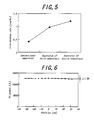
- Fig. 5 is a graph showing film growth rates of AIN films fabricated by using the fabricating apparatuses in the third and the fourth embodiments shown in Figs. 3 and 4, respectively, in comparison with the ones fabricated by using a conventional fabricating apparatus.
- the same condition is employed.
- the film growth rate was only 0.5 ⁇ m/hr.
- the film-forming rate is developed to about 1 ⁇ m/hr.
- the film growth rate is developed to about 1.2 ⁇ m.
- Fig. 6 is a graph showing a distribution in thickness of an AlN film fabricated on a 3-inch wafer by using the apparatus of the fourth embodiment shown in Fig. 4.
- the zero point of the abscissa axis designates the center of the wafer, and thus, the abscissa itself designates the distance of the center on the wafer.
- the vertical axis designates the thickness of the AlN film in order of angstrom.
- the distribution in thickness on the 3-inch wafer is repressed within 1.8%, and thus, it is turned out that the AlN film can be formed uniformly on such a larger substrate by using the apparatus of the present invention.
- the substrate 12 may be made of oxide single crystal such as ZnO single crystal, LiAlO 2 single crystal, LiGaO 2 single crystal, MgAl 2 O 4 single crystal, or MgO single crystal, IV single crystal or IV-IV single crystal such as Si single crystal or SiC single crystal, III-V single crystal such as GaAs single crystal.
- oxide single crystal such as ZnO single crystal, LiAlO 2 single crystal, LiGaO 2 single crystal, MgAl 2 O 4 single crystal, or MgO single crystal, IV single crystal or IV-IV single crystal such as Si single crystal or SiC single crystal, III-V single crystal such as GaAs single crystal.
- AlN single crystal, GaN single crystal or AlGaN single crystal, and boride single crystal such as ZrB 2 .
- the substrate may be made of an epitaxial substrate composed of a base material made of the above-mentioned single crystal and an epitaxial film made of oxide single crystal such as ZnO single crystal or MgO single crystal, IV single crystal or IV-IV single crystal such as Si single crystal or SiC single crystal, III-V single crystal such as GaAs single crystal, InP single crystal, AlN single crystal, GaN single crystal or AlGaN single crystal, and boride single crystal such as ZrB 2 .
- oxide single crystal such as ZnO single crystal or MgO single crystal
- IV single crystal or IV-IV single crystal such as Si single crystal or SiC single crystal
- III-V single crystal such as GaAs single crystal, InP single crystal, AlN single crystal, GaN single crystal or AlGaN single crystal
- boride single crystal such as ZrB 2 .
- the cooling jackets 51 and 52 made of stainless steel are provided on the outer side of the reactor 11, the reactor 11 itself may be partially made as a cooling jacket.
- the reactor is made of quartz and the cooling jacket is made of stainless steel, the configuration of the apparatus can be simplified, and the cost of the apparatus can be lowered. Then, the fabricating cost of the III-V nitride film can be reduced due to the easy maintenance.
- a substrate is set on a susceptor installed in a reactor arranged horizontally. Then, a cooling jacket is provided at the opposite portion of the inner wall of the reactor to the substrate. By flowing a given cooling medium through the cooling jacket with a pump connected to the jacket, at least the opposite portion of the inner wall is cooled down, to inhibit the reaction between raw material gases introduced into the reactor. As a result, in fabricating a III-V nitride film, the film growth rate is developed and the crystal quality is developed.
Landscapes
- Chemical & Material Sciences (AREA)
- Engineering & Computer Science (AREA)
- Materials Engineering (AREA)
- Metallurgy (AREA)
- Organic Chemistry (AREA)
- Chemical Kinetics & Catalysis (AREA)
- General Chemical & Material Sciences (AREA)
- Mechanical Engineering (AREA)
- Crystallography & Structural Chemistry (AREA)
- Inorganic Chemistry (AREA)
- Chemical Vapour Deposition (AREA)
- Crystals, And After-Treatments Of Crystals (AREA)
Abstract
Description
As the cooling medium, water may be exemplified.
In this case, the whole of the reactor can be cooled down effectively.
The introduced trimethylaluminum gas and the introduced ammonia gas are also introduced into the center region of the reactor through separated guiding
The vertical axis designates the thickness of the AlN film in order of angstrom.
As is apparent from Fig. 6, the distribution in thickness on the 3-inch wafer is repressed within 1.8%, and thus, it is turned out that the AlN film can be formed uniformly on such a larger substrate by using the apparatus of the present invention.
Claims (12)
- A method for fabricating a III-V nitride film, comprising the steps of:preparing a reactor horizontally,setting a substrate onto a susceptor installed in the reactor,heating the substrate to a predetermined temperature,directly cooling at least the portion of the inner wall of the reactor opposite to the substrate, andintroducing a III raw material gas and a V raw material gas with a carrier gas onto the substrate, and thus, fabricating a III-V nitride film by a MOCVD method.
- A fabricating method as defined in claim 1, wherein the susceptor is set on the bottom wall of the reactor, and the opposite portion of the top wall of the reactor to the substrate set on the susceptor is cooled down.
- A fabricating method as defined in claim 1 or 2, wherein the upper stream of the reactor from the substrate set on the susceptor is cooled down.
- A fabricating method as defined in claim 1 or 2, wherein the whole of the reactor is cooled down.
- A fabricating method as defined in any one of claims 1-4, wherein the III-V nitride film is an Al-rich AlxGayInzN (x+y+z=1, x>0.5, y≥0. Z≥0) film.
- A fabricating method as defined in any one of claims 1-4, wherein the III-V nitride film is an AlN film.
- An apparatus for fabricating a III-V nitride film by a MOCVD method, comprising:a reactor prepared horizontally,a susceptor to hold a substrate thereon installed in the reactor,a heater to heat the substrate to a predetermined temperature via the susceptor, anda cooling means to directly cool down at least the portion of the inner wall of the reactor opposite to the substrate.
- A fabricating apparatus as defined in claim 7, wherein the cooling means includes a cooling jacket, a pump to flow a given cooling medium through the cooling jacket and a cooling medium temperature-controlling means to control the temperature of the cooling medium.
- A fabricating apparatus as defined in claim 7, wherein the cooling jacket is made of stainless steel and the reactor is made of quartz.
- A fabricating apparatus as defined in any one of claims 7-9, wherein the cooling means is provided over the reactor entirely.
- A fabricating apparatus as defined in any one of claims 7-10, further comprising a housing on the outer side of the reactor, wherein the cooling means is provided on the outer side of the housing.
- A fabricating apparatus as defined in any one of claims 7-11, further comprising another cooling means at the upper stream of the reactor from the substrate set on the susceptor.
Applications Claiming Priority (4)
| Application Number | Priority Date | Filing Date | Title |
|---|---|---|---|
| JP2000377547 | 2000-12-12 | ||
| JP2000377547 | 2000-12-12 | ||
| JP2001340945 | 2001-11-06 | ||
| JP2001340945A JP3607664B2 (en) | 2000-12-12 | 2001-11-06 | III-V nitride film manufacturing apparatus |
Publications (3)
| Publication Number | Publication Date |
|---|---|
| EP1215308A2 true EP1215308A2 (en) | 2002-06-19 |
| EP1215308A3 EP1215308A3 (en) | 2008-01-23 |
| EP1215308B1 EP1215308B1 (en) | 2010-06-16 |
Family
ID=26605675
Family Applications (1)
| Application Number | Title | Priority Date | Filing Date |
|---|---|---|---|
| EP01129551A Expired - Lifetime EP1215308B1 (en) | 2000-12-12 | 2001-12-11 | A method for fabricating a III-V nitride film and an apparatus for fabricating the same |
Country Status (7)
| Country | Link |
|---|---|
| US (2) | US6709703B2 (en) |
| EP (1) | EP1215308B1 (en) |
| JP (1) | JP3607664B2 (en) |
| KR (1) | KR100449787B1 (en) |
| AT (1) | ATE471397T1 (en) |
| DE (1) | DE60142386D1 (en) |
| TW (1) | TW518670B (en) |
Families Citing this family (25)
| Publication number | Priority date | Publication date | Assignee | Title |
|---|---|---|---|---|
| JP3607664B2 (en) * | 2000-12-12 | 2005-01-05 | 日本碍子株式会社 | III-V nitride film manufacturing apparatus |
| JP2004363456A (en) | 2003-06-06 | 2004-12-24 | Toshiba Corp | Semiconductor device manufacturing method and manufacturing apparatus |
| CN100510167C (en) * | 2004-12-30 | 2009-07-08 | 中国科学院半导体研究所 | Inverse baking deposition structure in chemical vapor deposition equipment for metal organic matter |
| CN100344532C (en) * | 2005-03-25 | 2007-10-24 | 清华大学 | Carbon nanotube array growing device |
| JP4554469B2 (en) * | 2005-08-18 | 2010-09-29 | 日本碍子株式会社 | Group III nitride crystal forming method, laminate, and epitaxial substrate |
| KR20080037606A (en) * | 2005-08-25 | 2008-04-30 | 스미토모덴키고교가부시키가이샤 | Method for producing Bainian 1-hex (0≤x≤1) crystals, Bainian1-hex (0≤x≤1) crystal substrates, method for producing Baan crystals, Ban crystal substrates and products |
| WO2008130448A2 (en) | 2006-11-22 | 2008-10-30 | S.O.I.Tec Silicon On Insulator Technologies | Temperature-controlled purge gate valve for chemical vapor deposition chamber |
| US9580836B2 (en) | 2006-11-22 | 2017-02-28 | Soitec | Equipment for high volume manufacture of group III-V semiconductor materials |
| DE112008000279T5 (en) * | 2007-01-31 | 2010-04-01 | Sumitomo Chemical Co. Ltd. | Process for the preparation of group III-V compound semiconductors |
| DE102007009145A1 (en) * | 2007-02-24 | 2008-08-28 | Aixtron Ag | Device for depositing crystalline layers optionally by means of MOCVD or HVPE |
| JP4899958B2 (en) * | 2007-03-19 | 2012-03-21 | 日立電線株式会社 | Film forming method and film forming apparatus |
| JP4466723B2 (en) * | 2007-11-21 | 2010-05-26 | 住友電気工業株式会社 | Metalorganic vapor phase epitaxy system |
| US20090197424A1 (en) * | 2008-01-31 | 2009-08-06 | Hitachi Kokusai Electric Inc. | Substrate processing apparatus and method for manufacturing semiconductor device |
| CN101924023A (en) * | 2009-06-09 | 2010-12-22 | 日本派欧尼株式会社 | Vapor Phase Growth Apparatus for Group III Nitride Semiconductors |
| JP5409413B2 (en) * | 2010-01-26 | 2014-02-05 | 日本パイオニクス株式会社 | III-nitride semiconductor vapor phase growth system |
| JP2013115313A (en) * | 2011-11-30 | 2013-06-10 | Stanley Electric Co Ltd | Crystal growth apparatus |
| US8603898B2 (en) | 2012-03-30 | 2013-12-10 | Applied Materials, Inc. | Method for forming group III/V conformal layers on silicon substrates |
| JP5940375B2 (en) * | 2012-06-01 | 2016-06-29 | シャープ株式会社 | Vapor growth apparatus and method for manufacturing nitride semiconductor light emitting device |
| TWI565825B (en) * | 2012-06-07 | 2017-01-11 | 索泰克公司 | Gas injection components for deposition systems and related methods |
| US9941295B2 (en) | 2015-06-08 | 2018-04-10 | Sandisk Technologies Llc | Method of making a three-dimensional memory device having a heterostructure quantum well channel |
| US9425299B1 (en) | 2015-06-08 | 2016-08-23 | Sandisk Technologies Llc | Three-dimensional memory device having a heterostructure quantum well channel |
| US9721963B1 (en) | 2016-04-08 | 2017-08-01 | Sandisk Technologies Llc | Three-dimensional memory device having a transition metal dichalcogenide channel |
| US9818801B1 (en) | 2016-10-14 | 2017-11-14 | Sandisk Technologies Llc | Resistive three-dimensional memory device with heterostructure semiconductor local bit line and method of making thereof |
| JP7368845B2 (en) * | 2020-03-10 | 2023-10-25 | 国立大学法人広島大学 | How to decompose sodium oxide |
| JP7621834B2 (en) | 2021-03-04 | 2025-01-27 | 住友電工デバイス・イノベーション株式会社 | Method and apparatus for growing a semiconductor layer |
Family Cites Families (19)
| Publication number | Priority date | Publication date | Assignee | Title |
|---|---|---|---|---|
| US4047496A (en) * | 1974-05-31 | 1977-09-13 | Applied Materials, Inc. | Epitaxial radiation heated reactor |
| JPH0421780A (en) * | 1990-05-14 | 1992-01-24 | Sharp Corp | Vapor growth device |
| TW209253B (en) * | 1990-09-21 | 1993-07-11 | Nidden Aneruba Kk | |
| JPH11150249A (en) * | 1997-11-16 | 1999-06-02 | Anelva Corp | Method for forming uneven polysilicon layer, substrate processing apparatus used for implementing the method, and semiconductor memory device |
| US6440221B2 (en) * | 1996-05-13 | 2002-08-27 | Applied Materials, Inc. | Process chamber having improved temperature control |
| KR100200705B1 (en) * | 1996-06-08 | 1999-06-15 | 윤종용 | Manufacture apparatus of semiconductor device, process condition of manufacture apparatus, method of manufacturing capacitor using the same |
| KR100200728B1 (en) * | 1996-09-18 | 1999-06-15 | Samsung Electronics Co Ltd | Chamber of semiconductor apparatus |
| JPH10167884A (en) * | 1996-12-03 | 1998-06-23 | Nissin Electric Co Ltd | Chemical vapor deposition equipment |
| JP3917237B2 (en) * | 1997-05-20 | 2007-05-23 | 東京エレクトロン株式会社 | Resist film forming method |
| US6276072B1 (en) * | 1997-07-10 | 2001-08-21 | Applied Materials, Inc. | Method and apparatus for heating and cooling substrates |
| US5997649A (en) * | 1998-04-09 | 1999-12-07 | Tokyo Electron Limited | Stacked showerhead assembly for delivering gases and RF power to a reaction chamber |
| KR100297573B1 (en) * | 1998-04-09 | 2001-10-25 | 박근섭 | Reaction furnace for fabricating the third to the fifth group compound semiconductor |
| JP2000012463A (en) * | 1998-06-17 | 2000-01-14 | Mitsubishi Electric Corp | Film forming equipment |
| US6218280B1 (en) * | 1998-06-18 | 2001-04-17 | University Of Florida | Method and apparatus for producing group-III nitrides |
| JP2000138168A (en) * | 1998-10-29 | 2000-05-16 | Shin Etsu Handotai Co Ltd | Semiconductor wafer and vapor phase growth equipment |
| US6331212B1 (en) * | 2000-04-17 | 2001-12-18 | Avansys, Llc | Methods and apparatus for thermally processing wafers |
| JP5049443B2 (en) * | 2000-04-20 | 2012-10-17 | 東京エレクトロン株式会社 | Heat treatment system |
| JP2001345268A (en) * | 2000-05-31 | 2001-12-14 | Matsushita Electric Ind Co Ltd | Semiconductor manufacturing apparatus and semiconductor manufacturing method |
| JP3607664B2 (en) * | 2000-12-12 | 2005-01-05 | 日本碍子株式会社 | III-V nitride film manufacturing apparatus |
-
2001
- 2001-11-06 JP JP2001340945A patent/JP3607664B2/en not_active Expired - Lifetime
- 2001-11-22 TW TW090128930A patent/TW518670B/en not_active IP Right Cessation
- 2001-12-06 US US10/010,945 patent/US6709703B2/en not_active Expired - Lifetime
- 2001-12-11 DE DE60142386T patent/DE60142386D1/en not_active Expired - Lifetime
- 2001-12-11 EP EP01129551A patent/EP1215308B1/en not_active Expired - Lifetime
- 2001-12-11 AT AT01129551T patent/ATE471397T1/en not_active IP Right Cessation
- 2001-12-11 KR KR10-2001-0078086A patent/KR100449787B1/en not_active Expired - Lifetime
-
2003
- 2003-12-16 US US10/737,602 patent/US7955437B2/en not_active Expired - Fee Related
Also Published As
| Publication number | Publication date |
|---|---|
| DE60142386D1 (en) | 2010-07-29 |
| EP1215308B1 (en) | 2010-06-16 |
| EP1215308A3 (en) | 2008-01-23 |
| JP3607664B2 (en) | 2005-01-05 |
| KR20020046951A (en) | 2002-06-21 |
| JP2002246323A (en) | 2002-08-30 |
| TW518670B (en) | 2003-01-21 |
| US20040132298A1 (en) | 2004-07-08 |
| US7955437B2 (en) | 2011-06-07 |
| US20020124965A1 (en) | 2002-09-12 |
| US6709703B2 (en) | 2004-03-23 |
| KR100449787B1 (en) | 2004-09-22 |
| ATE471397T1 (en) | 2010-07-15 |
Similar Documents
| Publication | Publication Date | Title |
|---|---|---|
| EP1215308B1 (en) | A method for fabricating a III-V nitride film and an apparatus for fabricating the same | |
| US7906411B2 (en) | Deposition technique for producing high quality compound semiconductor materials | |
| EP1184488B1 (en) | An apparatus for fabricating a III-V nitride film and a method for fabricating the same | |
| US8382898B2 (en) | Methods for high volume manufacture of group III-V semiconductor materials | |
| US9038565B2 (en) | Abatement of reaction gases from gallium nitride deposition | |
| EP2066496B1 (en) | Equipment for high volume manufacture of group iii-v semiconductor materials | |
| US8323407B2 (en) | Gallium trichloride injection scheme | |
| US9441311B2 (en) | Growth reactor for gallium-nitride crystals using ammonia and hydrogen chloride | |
| US20100242835A1 (en) | High volume delivery system for gallium trichloride | |
| US20090223441A1 (en) | High volume delivery system for gallium trichloride | |
| EP1160354A1 (en) | Apparatus and method for depositing semiconductor film | |
| US20130104802A1 (en) | Gallium trichloride injection scheme | |
| JPH09102461A (en) | Vapor phase growth equipment | |
| EP1207215B1 (en) | A method for fabricating a III-V nitride film and an apparatus for fabricating the same | |
| JP3472976B2 (en) | Method and apparatus for forming group III nitride semiconductor | |
| WO2008064085A2 (en) | Abatement system for gallium nitride reactor exhaust gases |
Legal Events
| Date | Code | Title | Description |
|---|---|---|---|
| PUAI | Public reference made under article 153(3) epc to a published international application that has entered the european phase |
Free format text: ORIGINAL CODE: 0009012 |
|
| AK | Designated contracting states |
Kind code of ref document: A2 Designated state(s): AT BE CH CY DE DK ES FI FR GB GR IE IT LI LU MC NL PT SE TR |
|
| AX | Request for extension of the european patent |
Free format text: AL;LT;LV;MK;RO;SI |
|
| PUAL | Search report despatched |
Free format text: ORIGINAL CODE: 0009013 |
|
| AK | Designated contracting states |
Kind code of ref document: A3 Designated state(s): AT BE CH CY DE DK ES FI FR GB GR IE IT LI LU MC NL PT SE TR |
|
| AX | Request for extension of the european patent |
Extension state: AL LT LV MK RO SI |
|
| RIC1 | Information provided on ipc code assigned before grant |
Ipc: C30B 29/40 20060101ALI20071217BHEP Ipc: H01L 21/205 20060101ALI20071217BHEP Ipc: C23C 16/30 20060101ALI20071217BHEP Ipc: C30B 25/02 20060101AFI20020325BHEP |
|
| 17P | Request for examination filed |
Effective date: 20080703 |
|
| AKX | Designation fees paid |
Designated state(s): AT BE CH CY DE DK ES FI FR GB GR IE IT LI LU MC NL PT SE TR |
|
| 17Q | First examination report despatched |
Effective date: 20081002 |
|
| GRAP | Despatch of communication of intention to grant a patent |
Free format text: ORIGINAL CODE: EPIDOSNIGR1 |
|
| GRAS | Grant fee paid |
Free format text: ORIGINAL CODE: EPIDOSNIGR3 |
|
| GRAA | (expected) grant |
Free format text: ORIGINAL CODE: 0009210 |
|
| AK | Designated contracting states |
Kind code of ref document: B1 Designated state(s): AT BE CH CY DE DK ES FI FR GB GR IE IT LI LU MC NL PT SE TR |
|
| REG | Reference to a national code |
Ref country code: CH Ref legal event code: EP |
|
| REG | Reference to a national code |
Ref country code: IE Ref legal event code: FG4D |
|
| REF | Corresponds to: |
Ref document number: 60142386 Country of ref document: DE Date of ref document: 20100729 Kind code of ref document: P |
|
| REG | Reference to a national code |
Ref country code: NL Ref legal event code: VDEP Effective date: 20100616 |
|
| PG25 | Lapsed in a contracting state [announced via postgrant information from national office to epo] |
Ref country code: SE Free format text: LAPSE BECAUSE OF FAILURE TO SUBMIT A TRANSLATION OF THE DESCRIPTION OR TO PAY THE FEE WITHIN THE PRESCRIBED TIME-LIMIT Effective date: 20100616 |
|
| PG25 | Lapsed in a contracting state [announced via postgrant information from national office to epo] |
Ref country code: FI Free format text: LAPSE BECAUSE OF FAILURE TO SUBMIT A TRANSLATION OF THE DESCRIPTION OR TO PAY THE FEE WITHIN THE PRESCRIBED TIME-LIMIT Effective date: 20100616 Ref country code: AT Free format text: LAPSE BECAUSE OF FAILURE TO SUBMIT A TRANSLATION OF THE DESCRIPTION OR TO PAY THE FEE WITHIN THE PRESCRIBED TIME-LIMIT Effective date: 20100616 |
|
| PG25 | Lapsed in a contracting state [announced via postgrant information from national office to epo] |
Ref country code: GR Free format text: LAPSE BECAUSE OF FAILURE TO SUBMIT A TRANSLATION OF THE DESCRIPTION OR TO PAY THE FEE WITHIN THE PRESCRIBED TIME-LIMIT Effective date: 20100917 Ref country code: CY Free format text: LAPSE BECAUSE OF FAILURE TO SUBMIT A TRANSLATION OF THE DESCRIPTION OR TO PAY THE FEE WITHIN THE PRESCRIBED TIME-LIMIT Effective date: 20100616 |
|
| PG25 | Lapsed in a contracting state [announced via postgrant information from national office to epo] |
Ref country code: NL Free format text: LAPSE BECAUSE OF FAILURE TO SUBMIT A TRANSLATION OF THE DESCRIPTION OR TO PAY THE FEE WITHIN THE PRESCRIBED TIME-LIMIT Effective date: 20100616 |
|
| PG25 | Lapsed in a contracting state [announced via postgrant information from national office to epo] |
Ref country code: PT Free format text: LAPSE BECAUSE OF FAILURE TO SUBMIT A TRANSLATION OF THE DESCRIPTION OR TO PAY THE FEE WITHIN THE PRESCRIBED TIME-LIMIT Effective date: 20101018 Ref country code: BE Free format text: LAPSE BECAUSE OF FAILURE TO SUBMIT A TRANSLATION OF THE DESCRIPTION OR TO PAY THE FEE WITHIN THE PRESCRIBED TIME-LIMIT Effective date: 20100616 |
|
| PG25 | Lapsed in a contracting state [announced via postgrant information from national office to epo] |
Ref country code: IT Free format text: LAPSE BECAUSE OF FAILURE TO SUBMIT A TRANSLATION OF THE DESCRIPTION OR TO PAY THE FEE WITHIN THE PRESCRIBED TIME-LIMIT Effective date: 20100616 |
|
| PLBE | No opposition filed within time limit |
Free format text: ORIGINAL CODE: 0009261 |
|
| STAA | Information on the status of an ep patent application or granted ep patent |
Free format text: STATUS: NO OPPOSITION FILED WITHIN TIME LIMIT |
|
| PG25 | Lapsed in a contracting state [announced via postgrant information from national office to epo] |
Ref country code: DK Free format text: LAPSE BECAUSE OF FAILURE TO SUBMIT A TRANSLATION OF THE DESCRIPTION OR TO PAY THE FEE WITHIN THE PRESCRIBED TIME-LIMIT Effective date: 20100616 |
|
| 26N | No opposition filed |
Effective date: 20110317 |
|
| REG | Reference to a national code |
Ref country code: DE Ref legal event code: R097 Ref document number: 60142386 Country of ref document: DE Effective date: 20110316 |
|
| PG25 | Lapsed in a contracting state [announced via postgrant information from national office to epo] |
Ref country code: MC Free format text: LAPSE BECAUSE OF NON-PAYMENT OF DUE FEES Effective date: 20101231 |
|
| REG | Reference to a national code |
Ref country code: CH Ref legal event code: PL |
|
| GBPC | Gb: european patent ceased through non-payment of renewal fee |
Effective date: 20101211 |
|
| REG | Reference to a national code |
Ref country code: FR Ref legal event code: ST Effective date: 20110831 |
|
| PG25 | Lapsed in a contracting state [announced via postgrant information from national office to epo] |
Ref country code: LI Free format text: LAPSE BECAUSE OF NON-PAYMENT OF DUE FEES Effective date: 20101231 Ref country code: IE Free format text: LAPSE BECAUSE OF NON-PAYMENT OF DUE FEES Effective date: 20101211 Ref country code: CH Free format text: LAPSE BECAUSE OF NON-PAYMENT OF DUE FEES Effective date: 20101231 Ref country code: FR Free format text: LAPSE BECAUSE OF NON-PAYMENT OF DUE FEES Effective date: 20110103 |
|
| PG25 | Lapsed in a contracting state [announced via postgrant information from national office to epo] |
Ref country code: GB Free format text: LAPSE BECAUSE OF NON-PAYMENT OF DUE FEES Effective date: 20101211 |
|
| PG25 | Lapsed in a contracting state [announced via postgrant information from national office to epo] |
Ref country code: LU Free format text: LAPSE BECAUSE OF NON-PAYMENT OF DUE FEES Effective date: 20101211 |
|
| PG25 | Lapsed in a contracting state [announced via postgrant information from national office to epo] |
Ref country code: TR Free format text: LAPSE BECAUSE OF FAILURE TO SUBMIT A TRANSLATION OF THE DESCRIPTION OR TO PAY THE FEE WITHIN THE PRESCRIBED TIME-LIMIT Effective date: 20100616 |
|
| PG25 | Lapsed in a contracting state [announced via postgrant information from national office to epo] |
Ref country code: ES Free format text: LAPSE BECAUSE OF FAILURE TO SUBMIT A TRANSLATION OF THE DESCRIPTION OR TO PAY THE FEE WITHIN THE PRESCRIBED TIME-LIMIT Effective date: 20100927 |
|
| PGFP | Annual fee paid to national office [announced via postgrant information from national office to epo] |
Ref country code: DE Payment date: 20201201 Year of fee payment: 20 |
|
| REG | Reference to a national code |
Ref country code: DE Ref legal event code: R071 Ref document number: 60142386 Country of ref document: DE |