EP1213753A1 - Ceramic substrate, ceramic heater, electrostatic chuck and wafer prober for use in semiconductor producing and inspecting devices - Google Patents
Ceramic substrate, ceramic heater, electrostatic chuck and wafer prober for use in semiconductor producing and inspecting devices Download PDFInfo
- Publication number
- EP1213753A1 EP1213753A1 EP00904018A EP00904018A EP1213753A1 EP 1213753 A1 EP1213753 A1 EP 1213753A1 EP 00904018 A EP00904018 A EP 00904018A EP 00904018 A EP00904018 A EP 00904018A EP 1213753 A1 EP1213753 A1 EP 1213753A1
- Authority
- EP
- European Patent Office
- Prior art keywords
- heating element
- ceramic substrate
- resistance heating
- ceramic
- heater
- Prior art date
- Legal status (The legal status is an assumption and is not a legal conclusion. Google has not performed a legal analysis and makes no representation as to the accuracy of the status listed.)
- Withdrawn
Links
Images


Classifications
-
- H—ELECTRICITY
- H10—SEMICONDUCTOR DEVICES; ELECTRIC SOLID-STATE DEVICES NOT OTHERWISE PROVIDED FOR
- H10P—GENERIC PROCESSES OR APPARATUS FOR THE MANUFACTURE OR TREATMENT OF DEVICES COVERED BY CLASS H10
- H10P72/00—Handling or holding of wafers, substrates or devices during manufacture or treatment thereof
- H10P72/70—Handling or holding of wafers, substrates or devices during manufacture or treatment thereof for supporting or gripping
- H10P72/74—Handling or holding of wafers, substrates or devices during manufacture or treatment thereof for supporting or gripping using temporarily an auxiliary support
-
- C—CHEMISTRY; METALLURGY
- C04—CEMENTS; CONCRETE; ARTIFICIAL STONE; CERAMICS; REFRACTORIES
- C04B—LIME, MAGNESIA; SLAG; CEMENTS; COMPOSITIONS THEREOF, e.g. MORTARS, CONCRETE OR LIKE BUILDING MATERIALS; ARTIFICIAL STONE; CERAMICS; REFRACTORIES; TREATMENT OF NATURAL STONE
- C04B35/00—Shaped ceramic products characterised by their composition; Ceramics compositions; Processing powders of inorganic compounds preparatory to the manufacturing of ceramic products
-
- C—CHEMISTRY; METALLURGY
- C04—CEMENTS; CONCRETE; ARTIFICIAL STONE; CERAMICS; REFRACTORIES
- C04B—LIME, MAGNESIA; SLAG; CEMENTS; COMPOSITIONS THEREOF, e.g. MORTARS, CONCRETE OR LIKE BUILDING MATERIALS; ARTIFICIAL STONE; CERAMICS; REFRACTORIES; TREATMENT OF NATURAL STONE
- C04B35/00—Shaped ceramic products characterised by their composition; Ceramics compositions; Processing powders of inorganic compounds preparatory to the manufacturing of ceramic products
- C04B35/515—Shaped ceramic products characterised by their composition; Ceramics compositions; Processing powders of inorganic compounds preparatory to the manufacturing of ceramic products based on non-oxide ceramics
- C04B35/58—Shaped ceramic products characterised by their composition; Ceramics compositions; Processing powders of inorganic compounds preparatory to the manufacturing of ceramic products based on non-oxide ceramics based on borides, nitrides, i.e. nitrides, oxynitrides, carbonitrides or oxycarbonitrides or silicides
- C04B35/581—Shaped ceramic products characterised by their composition; Ceramics compositions; Processing powders of inorganic compounds preparatory to the manufacturing of ceramic products based on non-oxide ceramics based on borides, nitrides, i.e. nitrides, oxynitrides, carbonitrides or oxycarbonitrides or silicides based on aluminium nitride
-
- H—ELECTRICITY
- H10—SEMICONDUCTOR DEVICES; ELECTRIC SOLID-STATE DEVICES NOT OTHERWISE PROVIDED FOR
- H10P—GENERIC PROCESSES OR APPARATUS FOR THE MANUFACTURE OR TREATMENT OF DEVICES COVERED BY CLASS H10
- H10P72/00—Handling or holding of wafers, substrates or devices during manufacture or treatment thereof
- H10P72/70—Handling or holding of wafers, substrates or devices during manufacture or treatment thereof for supporting or gripping
- H10P72/72—Handling or holding of wafers, substrates or devices during manufacture or treatment thereof for supporting or gripping using electrostatic chucks
- H10P72/722—Details of electrostatic chucks
Definitions
- the present invention relates essentially to the ceramic substrate, ceramic heater, electrostatic chuck and wafer prober for semiconductor manufacture and/or inspection and more particularly to a ceramic substrate for semiconductor manufacture and/or inspection which is conducive to the prevention of electrical errors, decrease in electrostatic chucking force, generation of particles, and circuit defects.
- Semiconductor devices are manufactured through a process which comprises coating a photosensitive resin as an etching resist on a semiconductor wafer and etching the uncoated area.
- the photosensitive resin is applied in the form of a liquid to the surface of a semiconductor wafer by means of a spin coater or the like, it must be dried after coating to dissipate the solvent etc. and the thus-coated semiconductor wafer is set on a heater and heated. It is also necessary to heat the silicon wafer by, for example, sputtering.
- the conventional metallic heater heretofore used for this purpose comprises a resistance heating element disposed on the reverse side of an aluminum plate.
- the heater plate must be as thick as about 15 mm. This is because a thin metal plate undergoes thermal expansion on the heating mode to develop a curl and strains to damage or tip the semiconductor wafer placed on the metal plate. However, increasing the thickness of the heater plate leads to increases in heater weight and bulk.
- the heater temperature is controlled by varying the voltage and current applied to the resistance heating element, the great thickness of the metal plate causes the problem that the temperature of the heater plate cannot timely follow changes in voltage and current values, thus making temperature control difficult.
- Japanese Kokai Publication Hei-9-306642 and Japanese Kokai Publication Hei-4-324276 proposed ceramic heaters each comprising a substrate board comprising AlN, which is a non-oxide ceramic material of high thermal conductivity and high strength, and a resistance heating element formed internally of said substrate board.
- JP 2798570 discloses an electrostatic chuck comprising an AlN substrate, a resistance heating element formed therein, and, for the purpose of attracting and setting in position a semiconductor wafer on a heater, static electrodes as embedded in said AlN substrate.
- the inventors scrutinized these problems inherent in the prior art and found surprisingly that the cause of the troubles lies in the ⁇ -rays radiated from the AlN substrate and that by controlling the level of those ⁇ -rays below a given value, the erratic action and the decrease in electrostatic chucking force can be prevented, the deposition of ceramic particles on the semiconductor wafer surface be minimized and the incidence of circuit defects in the semiconductor wafer reduced to substantial nil.
- the present invention has been developed on the basis of the above findings.
- the present invention is directed to a ceramic substrate for semiconductor manufacture and/or inspection wherein the level of ⁇ -rays radiated from the surface thereof is not higher than 0.250c/cm 2 ⁇ hr and substantially within the range of 0.0001 to 0.250c/cm 2 ⁇ hr.
- the present invention is further directed to a ceramic heater for the heating of semiconductor wafers or other semiconductor products, comprising a ceramic substrate and a heating element either on the surface or internally thereof, wherein the level of ⁇ -rays radiated from the heating surface of said ceramic substrate is not higher than 0.250c/cm 2 ⁇ hr and substantially within the range of 0.0001 to 0.250c/cm 2 ⁇ hr.
- the present invention is further directed to an electrostatic chuck comprising a ceramic substrate and electrodes (static electrodes) embedded therein wherein the level of ⁇ -rays radiated from the surface of said ceramic substrate is not higher than 0.250c/cm 2 ⁇ hr and substantially within the range of 0.0001 to 0.250c/cm 2 ⁇ hr.
- the present invention is further directed to a wafer prober comprising a ceramic substrate and a conductor layer on the surface thereof wherein the level of ⁇ -rays radiated from said surface, the surface on which said conductor layer is formed, is not higher than 0.250c/cm 2 ⁇ hr and substantially within the range of 0.0001 to 0.250c/cm 2 ⁇ hr.
- the inventors of the present invention energetically explored into the problems with the prior art and, as mentioned above, found surprisingly that the ⁇ -rays radiated from the ceramic substrate are causative of those problems.
- the ⁇ -rays generated from the ceramic substrate create many electron-hole pairs in the semiconductor wafer.
- the semiconductor wafer itself is statically charged and this statistic electricity attracts particles from the ceramic substrate or triggers erratic actions of the ceramic heater and wafer prober due to the thermocouples embedded in the ceramic substrate.
- the electrostatic chuck electricity generated by the chuck electrodes is cancelled, thus detracting from the chucking force.
- the problems can be overcome by controlling the emission level of ⁇ -rays from the surface (carrying a conductor layer) of the ceramic substrate, regardless of whether the problems are associated with a ceramic heater, an electrostatic chuck or a wafer prober.
- thermocouples When the ceramic substrate is applied to a ceramic heater, thermocouples are disposed in the ceramic substrate but if the emission level of ⁇ -rays exceeds 0.250c/cm 2 ⁇ hr, the ⁇ -rays will impinge on the semiconductor wafer to form electron-hole pairs , which are causative of the static electricity, and the resulting static electricity creates electric noises in the thermocouples to cause an erratic temperature detection leading to an erratic operation of the heater. Such an erratic operation causes a delay in the time required for the temperature of the wafer-mounting surface to reach a steady level.
- the ⁇ -rays impinging on the semiconductor wafer produce electron-hole pairs in the semiconductor wafer, which results in the occurrence of static electricity, and the resultant static electricity attracts the particles dislodged from the ceramic substrate to the semiconductor wafer. This attraction of particles causes circuit defects in the masked-exposure process.
- the ceramic substrate for semiconductor manufacture and inspection according to the present invention is characterized in that the level of ⁇ -rays radiated from the semiconductor wafer surface (semiconductor wafer mounting surface, wafer heating surface or conductor layer surface) is not higher than 0.250c/cm 2 ⁇ hr and substantially within the range of 0.0001 to 0.250c/cm 2 ⁇ hr.
- the number of deposited particles can be reduced to 10/cm 2 or less.
- the thickness of the ceramic substrate is preferably 0.5 to 50 mm. If the thickness is less than 0.5 mm, the reduced strength will increase the risk for breakage. On the other hand, if the thickness exceeds 50 mm, the poor transfer of heat will sacrifice the heating efficiency.
- the optimum thickness range is 20 mm or less. This is because the internal level of ⁇ -rays can be reduced.
- the ceramic substrate is preferably in the form of a disk with a diameter of not less than 200 mm. Ceramic substrates having such large areas are more probable to cause troubles related with ⁇ -rays so that the effect of the invention is more pronounced.
- the ceramic substrate is preferably free of pores but, if it is porous, the porosity rate is preferably not greater than 5% and the maximum pore diameter is preferably not more than 50 ⁇ m. If these limits are exceeded, the ⁇ -rays passing through the air entrapped in the pores produce a plasma to reduce the insulation resistance at high temperature (not less than 200 °C).
- the ceramic heater according to the present invention comprises a heating element formed on the surface or internally of a ceramic substrate wherein the level of ⁇ -rays radiated from the surface of said ceramic substrate is not higher than 0.250c/cm 2 ⁇ hr and substantially within the range of 0.0001 to 0.250c/cm 2 ⁇ hr.
- the ceramic heater of the present invention wherein the level of ⁇ -rays radiated from the surface of the ceramic substrate is not higher than 0.025c/cm 2 ⁇ hr, is free from the disadvantage that the creation of electron-hole pairs in the semiconductor wafer caused by the ⁇ -rays would affect temperature data through the consequent charging of the resultant static electrocity and/or direct introduction of thermoelectrical noise to the thermocouples. Furthermore, if the level of ⁇ -rays is confined to not more than 0.025c/cm 2 ⁇ hr, static electrocity on the semiconductor wafer is not likely to occur, therefore the deposition of ceramic particles thereon can be reduced.
- the level of ⁇ -ray emission is equal to nil but it is technically and economically difficult to achieve an emission level less than 0.0001c/cm 2 ⁇ hr.
- the emission level of ⁇ -rays exceeds 0.025c/cm 2 ⁇ hr, ceramic particles tend to be deposited on the semiconductor wafer due to the static charge generated by ⁇ - rays so that the semiconductor wafer may sustain a damage crippling its function.
- the cause of ⁇ -rays is the radioactive U and Th in the starting material alumina or silica for the nitride. Therefore, U and Th are removed from the starting material alumina and silica and the objective nitride ceramics are synthesized by, for example, the reductive nitriding method.
- the method of removing U and Th may be a process which, as described in "Synopsis of Lectures at Association of Powder Metallurgy, p. 114, Spring 1980", comprises impregnating a porous ⁇ -FeO 3 powder having a mean particle diameter of 2 to 3 ⁇ m with an alcoholic solution of titanium isopropoxide, hydrolyzing the alkoxide to cause the resulting titanium hydroxide etc. to be adsorbed on the ⁇ -FeO 3 for use as a U adsorbent to be dispersed in a starting material solution.
- the subsequent process comprises dispersing the U adsorbent in an aqueous solution of sodium aluminate derived from bauxite (Al 2 O 3 ) to let U be adsorbed under basic conditions, separating the adsorbent, converting the sodium aluminate to aluminum hydroxide and to be precipitated, then drying and firing it to give alumina.
- the alumina etc. thus obtained are nitrided by the reductive nitriding method.
- the reductive nitriding method comprises reducing SiO 2 and Al 2 O 3 with carbon, such as carbon black, and simultaneously reacting them with nitrogen gas.
- Japanese Kokai Publication Hei-9-48668 discloses a sintered aluminum nitride for semiconductor production apparatuses as synthesized by a direct nitriding method or an indirect nitriding method, the literature does not refer to the starting material alumina. Moreover, because U and Th are derived from bauxite, the amounts of U and Th cannot be reduced by the mere direct nitriding method.
- the ceramic heater of the present invention is a ceramic heater for heating semiconductor wafers and comprises a heating element on the surface or internally of a nitride ceramic substrate.
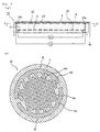
- Fig. 1 is a schematic bottom view showing a ceramic heater of the invention and Fig. 2 is a partial section view of the same on exaggerated scale.
- the ceramic substrate (hereinafter referred to as heater plate) 11 comprising nitride ceramics is prepared in the form of a disk and a resistance heating element 12 is formed internally of said heater plate 11 in a concentric circular pattern so that the wafer-heating surface (top side) of the heater plate 11 may be uniformly heated all over.
- the resistance heating element 12 comprises a plurality of circular patterns with each two adjacent circles being coupled to form a single wire which is to be connected to external terminals 13, one of which serves as an input terminal with the other serving as an output terminal.
- the heater plate 11 is further formed with through holes 15 for accepting support pins 16 for supporting a semiconductor wafer 19 and further with bottomed holes 14 in which temperature probes are to be embedded.
- the resistance heating element 12 is disposed internally of the heater plate 11 in the ceramic heater 10 illustrated in Figs. 1 and 2, the resistance heating element 12 may be formed on the bottom surface of the heater plate 11.
- the ceramic heater 10 of the present invention is based on nitride ceramics.
- nitride ceramics are lower than metals in the coefficient of thermal expansion, they will not easily curl or warp so that a lighter and thinner heater plate 11 can be provided.
- the heater plate 11 is high in heat conductivity and thin by itself so that the surface temperature of the heater plate 11 quickly follows the change in temperature of the resistance heating element.
- the surface temperature of the heater plate 11 can be easily and accurately controlled.
- the ceramics mentioned above include nitride ceramics, oxide ceramics and carbide ceramics but nitride ceramics are particularly suitable.
- nitride ceramics are high in thermal conductivity and superior in the temperature rise-and-fall characteristic, they are used for the ceramic substrate on which a wafer is directly set or supported in close proximity with its surface.
- the beneficial effect of the present invention is particularly remarkable when a nitride ceramic substrate is employed.
- the nitride ceramic material mentioned above includes aluminum nitride, silicon nitride, boron nitride, titanium nitride and other nitride ceramics. These ceramics can be used independently or in combination.
- aluminum nitride is the most preferred because it has the highest heat conductivity of all, namely 180 W/m ⁇ K.
- Oxide ceramics includes silica and alumina among others, and carbide ceramics include silicon carbide, for instance.
- the resistance heating element 12 formed on the surface or internally of said nitride ceramic substrate is preferably divided into at least two circuits. By dividing the circuitry, the amount of heat to be generated can be adjusted by controlling the inputs to the respective component circuits, with the result that the temperature of the wafer-heating surface can be accordingly controlled.
- the pattern of the resistance heating element 12 may for example be a group of concentric circles, a vortex, a group of eccentric circles, or a serpentine form but the concentric pattern illustrated in Fig. 1 is preferred because a uniform temperature distribution can be obtained over the whole surface of the heater plate.
- the resistance heating element 12 is to be formed on the surface of the heater plate 11, it is preferable to use the method which comprises coating the surface of the heater plate 11 with a conductor containing paste containing a metal particle in a predetermined circuit pattern and sintering the resulting conductor containing paste layer to bake the metal particle on the surface of the heater plate 11. It is sufficient that this sintering be effected to the extent of the metal particles being fused to each other and with the ceramics.
- the thickness of the heating element is preferably 1 to 30 ⁇ m, more preferably 1 to 10 ⁇ m.
- its thickness is preferably 1 to 50 ⁇ m.
- the pattern width of the resistance heating element is preferably 0.1 to 20 mm, more preferably 0.1 to 5 mm.
- the pattern width of the resistance heating element is 5 to 20 ⁇ m.
- the resistance value of the resistance heating element 12 can be freely adjusted by varying the pattern thickness and width but the above-mentioned ranges are most useful for practical purposes.
- the resistance heating element 12 should be greater in thickness and width when it is formed internally of the resistance heater plate 11. When the resistance heating element 12 is formed internally, the distance between the heating surface and the resistance heating element 12 is comparatively short, with the result that the temperature uniformity of the heating surface tends to be poor, thus making it necessary to increase the pattern width of the resistance heating element.
- the resistance heating element 12 when the resistance heating element 12 is to be disposed internally, its adhesion to nitride ceramics need not be taken into consideration, so that a high-melting metal such as tungsten or molybdenum or the carbide thereof can be used to increase the resistance.
- the thickness itself can be increased for the purpose of preventing a disconnection trouble, for instance. From these considerations, the pattern thickness and width of the resistance heating element 12 are preferably controlled within the above-mentioned ranges.
- the resistance heating element 12 may be rectangular or elliptic in sectional view but preferably has a flat surface.
- the flat surface is more efficient in the radiation of heat toward the wafer-heating surface and is less liable to cause a temperature gradient.
- the aspect ratio of the cross-section is preferably 10 to 5000.
- the resistance value of the resistance heating element 12 can be increased and a temperature uniformity on the heating surface can be insured.
- the use of an aspect ratio smaller than the above range leads to a relatively poor propagation of heat from the heater plate 11 in the wafer-heating direction so that a distribution of heat simulating the pattern of the resistance heating element 12 is produced on the heating surface.
- the aspect ratio is too large, a relatively high temperature will prevail in the area immediately above the center of the resistance heating element 12 so that a thermal distribution more or less simulating the pattern of the resistance heating element 12 is likewise produced on the heating surface. Therefore, in consideration of temperature distribution, the aspect ratio of the cross-section is preferably confined to the range of 10 to 5000.
- the aspect ratio is preferably 10 to 200 and when the resistance heating element 12 is to be formed internally of the heater plate 11, the preferred aspect ratio is 200 to 5000.
- That a larger aspect ratio is preferred when the resistance heating element 12 is formed internally of the heater plate 11 is because, as the resistance heating element 12 is internally disposed, the distance between the heating surface and the resistance heating element 12 is relatively decreased so that the uniformity of surface temperature distribution is also reduced, thus requiring a more flat geometry for the resistance heating element 12.
- the resistance heating element 12 When the resistance heating element 12 is to be formed in a biased position in thickness direction within the heater plate 11, it is preferably formed in a position close to the surface (bottom surface) opposite to the heating surface of the heater plate 11 and within the range of 50% through 99% of the distance from the heating surface to said bottom surface.
- the resistance heating element 12 will be too close to the heating surface so that a temperature gradient tends to be formed on the heating surface. Conversely, if the amount of offset is over 99%, the heater plate 11 itself tends to curl to destroy the semiconductor wafer.
- the resistance heating element 12 when the resistance heating element 12 is formed internally of the heater plate 11, the resistance heating element may comprise a plurality of layers.
- the patterns of the respective layers are preferably disposed in mutually complementary relation so that, when viewed from above the wafer-heating surface, the whole resistance heating element 12 can be observed without an overlap over the entire field of view.
- Typical of such layout is a staggered arrangement of the patterns.
- the conductor containing paste is not particularly restricted but is preferably a composition containing not only the metal particle or conductive ceramic particle required for electrical conductivity but also a resin, a solvent, a thickener and other additives.
- the metal particle mentioned above is preferably a powder of, for example, a noble metal (gold, silver, platinum, palladium), lead, tungsten, molybdenum or nickel. These metals can be used singly or in a combination of two or more species. Those metals are comparatively resistant to oxidation and have sufficiently high resistance to generate heat.
- a noble metal gold, silver, platinum, palladium
- lead tungsten
- molybdenum nickel
- the conductive ceramic particle includes tungsten carbide and molybdenum carbide powders. Those powders can be used each independently or in a combination of two or more species.
- the preferred particle diameter of said metal or conductive ceramic particle is 0.1 to 100 ⁇ m. If the powder is finer than 0.1 ⁇ m, it will be ready to be oxidized. On the other hand, if the limit of 100 ⁇ m is exceeded, the powder will not be easily sintered and the resistance value will be increased.
- the metal particle mentioned above may be spherical or flaky.
- a mixture of spherical and flaky powders may also be employed.
- the metal particle is flaky or a mixture of spherical and flaky particles
- the metal oxide added is held more effectively between the metal particles, with the consequent advantage that a firmer adhesion can be assured between the resistance heating element 12 and the nitride ceramics and that the resistance value can be increased.
- the resin for use in the conductor containing paste includes, for example, epoxy resin and phenolic resin.
- the solvent may for example be isopropyl alcohol.
- the thickener may for example be cellulose.
- the conductor containing paste is preferably a paste prepared by adding metal oxides to the starting metal particle so that the resistance heating element 12 will be a sintered body composed of the metal and metal oxide powders.
- the conductor containing paste is preferably a paste prepared by adding metal oxides to the starting metal particle so that the resistance heating element 12 will be a sintered body composed of the metal and metal oxide powders.
- the metal oxides mentioned above are preferably at least one kind of the members selected from the group consisting of lead oxide, zinc oxide, silica, boron oxide (B 2 O 3 ), alumina, yttria and titania.
- These oxides are capable of improving the adhesion between the metal particle and nitride ceramics without increasing the resistance value of the resistance heating element 12.
- the proportions of said lead oxide, zinc oxide, silica, boron oxide (B 2 O 3 ), alumina, yttria and titania in each 100 weight parts of the total metal oxide are 1 to 10 (weight parts; the same applies below) for lead oxide, 1 to 30 for silica, 5 to 50 for boron oxide, 20 to 70 for zinc oxide, 1 to 10 for alumina, 1 to 50 for yttria, and 1 to 50 for titania.
- the total of these oxides is preferably not more than 100 weight parts.
- the bonding of the metal particle to nitride ceramics in particular, can be improved.
- the addition amount of said metal oxide(s) relative to the metal particle is preferably not less than 0.1 weight %and less than 10 weight %.
- the area resistivity of the resistance heating element 12 formed by using a conductor containing paste of the above composition is preferably 1 to 45 m ⁇ / ⁇ .
- the area resistivity exceeds 45 m ⁇ / ⁇ , the generation of heat will be too great in relation to the level of voltage applied so that the generation of heat can hardly be controlled in the case of a heater plate 11 carrying the resistance heating element 12 on its surface. If the addition amount of said metal oxide (s) is not less than 10 weight %, the area resistivity will exceed 50 m ⁇ / ⁇ and the excessively increased heat generation will make temperature control difficult and the uniformity of temperature distribution will be sacrificed.
- a metal cover layer is preferably formed on the surface of the resistance heating element 12. Because the layer prevents oxidation of the sintered metal and consequent change in resistance value.
- the thickness of the metal cover layer thus formed is preferably 0.1 to 10 ⁇ m.
- the metal for use in the formation of said metal cover layer is not particularly restricted only provided that it is a non-oxidizable metal.
- it may for example be gold, silver, palladium, platinum or nickel.
- These metals can be used alone or in a combination of two or more species.
- nickel is particularly preferred.
- the resistance heating element 12 must, of course, be provided with terminals for electrical connection to a power source and since these terminals are generally attached to the resistance heating element 12 via a solder, a nickel layer is preferred because it prevents thermal diffusion of the solder.
- connecting terminals external terminals 13 made of Koval®, for instance, can be used.
- the resistance heating element 12 When the resistance heating element 12 is formed internally of the heater plate 11, the surface of the resistance heating element 12 will not be oxidized and, therefore, need not be covered. When the resistance heating element 12 is formed internally of the heater plate 11, the resistance heating element may be left partially exposed, or may be provided with conductor-filled through holes at its terminal positions for connecting and securing in position said external terminals.
- solder for use in connecting the external terminals various alloys such as silver-lead, lead-tin, bismuth-tin, etc. can be used.
- the preferred thickness of the solder layer is 0.1 to 50 ⁇ m. Within this range, firm solder connections can be obtained.
- the heater plate 11 may be provided with through holes 15 so that by inserting pins (not shown) into the through holes 15, the semiconductor wafer may be delivered to a transfer machine (not shown) or received from the transfer machine.
- the semiconductor wafer can be heated with a clearance of 50 to 500 ⁇ m maintained from the ceramic substrate. By providing this clearance, the wafer can be protected more or less from the influence of the surface temperature distribution of the ceramic substrate. In this mode of use, the wafer is supported with support pins 16 and heated in that position.
- nitride ceramic powder described above e.g. an aluminum nitride ceramic powder
- sintering aids such as yttria etc., a binder, and other components to prepare a slurry.
- This slurry is spray-dried and the resulting granules are placed in a metal mold or the like and compressed into a plate form to provide a raw formed body(green).
- the ceramic heater When the ceramic heater is to be provided with the function of an electrostatic chuck, a metal foil or the like for electrostatic chucking can be embedded in the raw formed body.
- the raw formed body is optionally formed with through holes for accepting said support pins for supporting a semiconductor wafer and, further, with bottomed holes in which temperature probes such as thermocouples are to be embedded.
- the above processing may be performed after the sintering operation.
- this raw formed body is heated and fired to be sintered and provide a ceramic substrate.
- a heater plate 11 is then prepared by machining this ceramic substrate.
- the ceramic substrate may be manufactured to the specified size so that it may directly be used as the heater plate 11 after firing.
- the heating temperature may be any suitable temperature not less than the sintering point of the ceramics but, in the case of nitride ceramics, a temperature within the range of 1000 to 2500 °C is used.
- the conductor containing paste is generally a highly viscous fluid comprising a metal particle, a resin and a solvent.
- the conductor containing paste layer is formed by printing the body with said conductor containing paste in the pattern corresponding to a resistance heating element by the screen printing technique, for instance. Since the resistance heating element is required to set the heater plate at a uniform temperature over its whole surface, it is preferably printed in a concentric circular pattern as illustrated in Fig. 1.
- the conductor containing paste layer be formed in such a manner that the resistance heating element 12 after sintering will have a rectangular section and a flat surface.
- the conductor containing paste layer printed on the bottom surface of the heater plate 11 is heated and fired to remove the resin and solvent, to sinter the metal particle onto the bottom surface of the heater plate 11, and thereby to form a resistance heating element 12.
- the heating temperature is preferably 500 to 1000 °C.
- the metal particle, heater plate and metal oxide(s) are integrally sintered to provide an improved bond between the resistance heating element and heater plate.
- the surface of the resistance heating element 12 is preferably provided with a metal cover layer.
- the metal cover layer can be formed by, for example, electrolytic plating, electroless plating or sputtering but, for mass production, electroless plating is the most suitable of all.
- terminals for electrical connection to a power source are attached by soldering.
- thermocouples are inserted into the bottomed holes 14 and secured in situ with a silver or gold brazing material and further sealed with a heat-resistant resin such as a polyimide resin to complete the manufacture of a ceramic heater.
- the nitride ceramic powder is mixed with the binder, solvent, etc. to prepare a paste, and using the paste, a green sheet is formed.
- the nitride ceramic powder as mentioned above includes an aluminum nitride powder, and where necessary, sintering aids such as yttria may be added.
- the binder is'preferably at least one member selected from the group consisting of acrylic binder, ethylcellulose, butylcellosolve and polyvinyl alcohol.
- the solvent is preferably at least one member selected from the group consisting of ⁇ -terpineol and glycol.
- the paste obtained by compounding those components is molded by the doctor blade method to provide said green sheet.
- the preferred thickness of the green sheet is 0.1 to 5 mm.
- the green sheet is formed with means serving as through holes 15 for accepting support pins for supporting a semiconductor wafer, means serving as bottomed holes in which temperature probes such as thermocouples are to be embedded, and means serving as conductor-filled through holes 18 for connecting the resistance heating element to external terminal pins.
- This processing may be carried out after formation of a green sheet laminate to be described below or after sintering of the laminate.
- the conductor containing paste containing a metal or conductive ceramic particle is printed.
- the conductor containing paste contains a metal or conductive ceramic particle.
- the mean particle diameter of tungsten or molybdenum powder is preferably 0.1 to 5 ⁇ m. If the mean particle diameter is less than 0.1 ⁇ m or over 5 ⁇ m, the printability of the conductor containing paste will be unsatisfactory.
- the conductor containing paste may for example be a composition (paste) comprising 85 to 87 weight parts of a metal or conductive ceramic particle, 1.5 to 10 weight parts of at least one kind of binder selected from the group consisting of acrylic binder, ethylcellulose, butylcellosolve and polyvinyl alcohol, and 1.5 to 10 weight parts of at least one kind of solvent selected from the group consisting of ⁇ -terpineol and glycol.
- a composition (paste) comprising 85 to 87 weight parts of a metal or conductive ceramic particle, 1.5 to 10 weight parts of at least one kind of binder selected from the group consisting of acrylic binder, ethylcellulose, butylcellosolve and polyvinyl alcohol, and 1.5 to 10 weight parts of at least one kind of solvent selected from the group consisting of ⁇ -terpineol and glycol.
- the green sheets not printed with the conductor containing paste are laminated on both sides of the green sheet printed with the conductor containing paste.
- this step it is arranged so that the number of green sheets to be laminated on the top side is larger than the number of green sheets to be laminated on the bottom side so that the resistance heating element will be located closer to the bottom side.
- the preferred number of green sheets to be laminated is 20 to 50 on the top side and 5 to 20 on the bottom side.
- the green sheet laminate is hot-pressed to sinter the green sheets and the conductor containing paste within the laminate.
- the heating temperature is preferably 1000 to 2000 °C and the pressure to be applied is preferably 100 to 200 kg/cm 2 .
- the heating operation is performed in an inert gas atmosphere.
- the inert gas may for example be argon gas or nitrogen gas.
- the bottomed holes for accepting temperature probes may be formed after this sintering operation.
- the bottomed holes can be formed by blasting, e.g. sandblasting, after surface polishing.
- terminals are attached to the conductor-filled through holes for connection to the internal resistance heating element, followed by heating for reflow.
- the heating temperature is preferably 200 to 500 °C.
- thermocouples as temperature probes are secured in position with a silver or gold brazing material and sealed with a heat-resistant resin such as polyimide resin to complete the manufacture of a ceramic heater.
- the electrostatic chuck of the invention comprises a nitride ceramic substrate and static electrodes embedded within said ceramic, wherein the level of ⁇ -rays radiated from the wafer-heating surface of said ceramic substrate is not higher than 0.250c/cm 2 ⁇ hr and substantially within the range of 0.0001 to 0.250c/cm 2 ⁇ hr.
- the nitride ceramic substrate for this electrostatic chuck of the present invention comprises the same material as the ceramic substrate for the ceramic heater of the present invention hereinbefore, and also manufactured in the same manner.
- the level of ⁇ -rays radiated from the wafer-mounting surface is substantially controlled to 0.0001 to 0.250c/cm 2 ⁇ hr so that the wafer surface is not scarcely charged by the impingement of ⁇ -rays.
- the static charge generated on the wafer by the static electrodes is substantially not cancelled so that the decrease in the force of attraction in accordance of the Johnson-Rahbeck effect can be prevented.
- the ⁇ -ray level is not higher than 0.025c/cm 2 ⁇ hr, the static electricity on the semiconductor wafer is scarcely generated and, therefore, the amount of deposition of particles is also reduced.
- the level of ⁇ -ray emission is equal to nil but it is technically and economically difficult to achieve an emission level less than 0.0001c/cm 2 ⁇ hr.
- the emission level of ⁇ -rays exceeds 0.025c/cm 2 ⁇ hr, ceramic particles tend to be deposited on the semiconductor wafer due to the static charge generated by ⁇ -rays so that the semiconductor wafer may sustain a damage crippling its function.
- Fig. 3 (a) is a schematic longitudinal section view of the electrostatic chuck and (b) is a sectional view of the same chuck as taken along the line A-A of (a).
- This electrostatic chuck 20 comprises a ceramic substrate 21, chuck positive electrode static layer 22 and chuck negative electrode static layer 23, disposed internally of said ceramic substrate 21, and a 5 to 1500 ⁇ m-thick ceramic dielectric film 40 formed on said electrodes.
- a resistance heating element 12 formed within said ceramic substrate 21 is a resistance heating element 12 so as to heat a silicon wafer 9.
- an RF electrode may be embedded in the ceramic substrate 21.
- the electrostatic chuck 20 is usually formed in a circular configuration in plan view, and disposed internally of the ceramic substrate 21 are the chuck positive electrode static layer 22 comprising a semi-circular segment 22a and a comb-shaped segment 22b and the chuck negative electrode static layer 23 similarly comprising a semi-circular segment 23a and a comb-shaped segment 23b, the two layers 22 and 23 being arranged face-to-face in such a manner that the teeth of the two comb-shaped segments 22b, 23b are in staggered relation.
- the chuck positive electrode static layer 22 and chuck negative electrode static layer 23 are connected to the + and - terminals, respectively, and a DC source and charged. Thereupon, the semiconductor wafer set on the electrostatic chuck is attracted by static electricity.
- the resistance heating element may be embedded internally of the ceramic substrate 21 as shown in Fig. 3 or formed on the surface (bottom side) of the ceramic substrate 21.
- the method of manufacturing the above electrostatic chuck is substantially identical to the method of manufacturing the ceramic heater except that the surface of said green sheet is coated with a conductor containing paste in the configurations of the chuck positive electrode static layer 22 and chuck negative electrode static layer 23 or a metal foil is embedded according to the patterns of said chuck positive electrode static layer 22 and chuck negative electrode static layer 23.
- the level of ⁇ -rays radiated from the wafer-mounting surface is controlled to 0.0001 to 0.250c/cm 2 ⁇ hr, whereby the noise signal derived from ⁇ -rays is hardly produced in the chuck top conductor layer, with the result that errors in the conduction test can be precluded.
- the semiconductor wafer is hardly charged electrostatically so that the deposition of particles on the wafer can be decreased.
- the chuck top conductor layer is formed on the surface of the ceramic substrate.
- the conduction test is performed by setting a wafer on the chuck top conductor layer and pressing a probe card carrying tester pins against the wafer.
- the noble metal layer formed on the chuck top conductor layer does not interfere with the current conduction to the reverse side of the wafer and prevents diffusion of boron and phosphorus in the chuck top conductor layer and of yttria, sodium etc. in the ceramics.
- the noble metal is preferably at least one member selected from among gold, silver, platinum and palladium.
- the chuck top is not caused to curl even if it is pressed by the tester pins of the probe card so that the chuck top layer may be made smaller in thickness than the case of the metal substrate.
- the chuck top may be designed to be smaller in thickness than the case of the metal substrate, the heat capacity may be reduced even though the heat conductivity of ceramics is low as compared with metals as the outcome, so that the temperature rise-and-fall characteristic can be improved.
- the preferred thickness of said chuck top conductor layer is 1 to 10 ⁇ m. If it is less than 1 ⁇ m, the layer will be too high in resistance to function as an electrode. On the other hand, if the limit of 10 ⁇ m is exceeded, the layer tends to peel off due to the strain in the conductor.
- At least one metal selected from among high-melting metals such as copper, titanium, chromium, nickel, noble metals (gold, silver, platinum, etc.), tungsten, molybdenum, etc. can be used.
- the chuck top conductor layer contains nickel, for this metal is high in hardness and is not easily deformed by the pressure of tester pins.
- the wafer prober according to the present invention is preferably equipped with a guard electrode and a ground electrode as embedded in the ceramic substrate.
- the guard electrode is intended to cancel stray capacitance in the measuring circuit, and the earth potential of the measuring circuit (that is the chuck top conductor layer) is applied thereto.
- the ground electrode is intended to cancel the noise from the temperature control means.
- the chuck top conductor layer-forming surface of the wafer prober according to the present invention is preferably formed with grooves and air suction holes.
- the wafer W can be attracted by setting the wafer and withdrawing air through the suction holes.
- the apparatuses for semiconductor manufacture and inspection according to the present invention can be put to use at a temperature ranging from 150 °C to 900 °C.
- Example 1 Manufacture of a ceramic heater having a heating element on its surface
- Example 2 Manufacture of an electrostatic chuck internally provided with a heating element and static electrodes
- the ⁇ -ray level was measured under the following conditions.
- the heater erratic action was evaluated by plotting the temperature data from the thermocouples to construct a temperature rise profile and checking for data markedly deviating from the profile.
- the electrostatic chucking force was measured with a load cell.
- the erratic action of the wafer prober was evaluated by performing a conduction test with it on 100 silicon wafers judged to be acceptable in the test using a commercial wafer prober having a metallic chuck top plate and checking if even one of the wafers was found to be rejected.
- the number of particles was generally 7 to 9/cm 2 but within the range of 0.048c/cm 2 ⁇ hr to 0.240c/cm 2 ⁇ hr, the number of particles was 20 to 30/cm 2 .
- the number of particles was not less than 120/cm 2 .
- the number of particles was not counted for the electrostatic chuck and wafer prober. This is because, in the case of electrostatic chucks, the deposition of particles attributable to the static electricity generated by the electrodes cannot be differentiated from the deposition caused by ⁇ -rays and, in the case of wafer probers, the silicon wafer is not brought into contact with the ceramics so that substantially no deposition of particles takes place.
- the ceramic heater, electrostatic chuck and wafer prober of the present invention are advantageous in that the emission level of ⁇ -rays is kept low enough to prevent the occurrence of erratic actions and decrease in chucking force in the case of the heater or the wafer prober and thus decreasing the number of particles deposited on the semiconductor wafer to thereby eliminate the risk for wafer circuit defects.
Landscapes
- Engineering & Computer Science (AREA)
- Chemical & Material Sciences (AREA)
- Ceramic Engineering (AREA)
- Organic Chemistry (AREA)
- Materials Engineering (AREA)
- Structural Engineering (AREA)
- Manufacturing & Machinery (AREA)
- Container, Conveyance, Adherence, Positioning, Of Wafer (AREA)
- Resistance Heating (AREA)
- Testing Or Measuring Of Semiconductors Or The Like (AREA)
- Surface Heating Bodies (AREA)
- Exposure And Positioning Against Photoresist Photosensitive Materials (AREA)
- Ceramic Products (AREA)
- Exposure Of Semiconductors, Excluding Electron Or Ion Beam Exposure (AREA)
Abstract
Description
wherein the level of α-rays radiated from the surface thereof is not higher than 0.250c/cm2·hr and substantially within the range of 0.0001 to 0.250c/cm2·hr.
wherein the level of α-rays radiated from the heating surface of said ceramic substrate is not higher than 0.250c/cm2·hr and substantially within the range of 0.0001 to 0.250c/cm2·hr.
wherein the level of α-rays radiated from the surface of said ceramic substrate is not higher than 0.250c/cm2·hr and substantially within the range of 0.0001 to 0.250c/cm2·hr.
wherein the level of α-rays radiated from said surface, the surface on which said conductor layer is formed, is not higher than 0.250c/cm2·hr and substantially within the range of 0.0001 to 0.250c/cm2·hr.
| U content (ppb) | Th content (ppb) | |
| Powder A | 4.5 | 0.9 |
| Powder B | 5.0 | 4.5 |
| Powder C | 51 | 26 |
| Powder D | 67 | 20 |
| Powder E | 150 | 20 |
| Powder F | 590 | 4 |
| Powder G | 600 | 5 |
| Powder H | 650 | 30 |
ACS-4000M
| Powder | Level of α-rays (c/cm2·hr) | Occurrence of erratic action | Chucking force (g/cm2) | Error in testing | Number of particles (piece/cm2) | |
| Ex. 1 | A | 0.001 | No | - | - | 7 |
| B | 0.005 | No | - | - | 9 | |
| C | 0.021 | No | - | - | 8 | |
| D | 0.027 | No | - | - | 7 | |
| E | 0.048 | No | - | - | 8 | |
| F | 0.210 | No | - | - | 20 | |
| G | 0.240 | No | - | - | 30 | |
| Ex. 2 | A | 0.001 | No | 125 | - | - |
| B | 0.005 | No | 120 | - | - | |
| C | 0.021 | No | 119 | - | - | |
| D | 0.027 | No | 118 | - | - | |
| E | 0.048 | No | 118 | - | - | |
| F | 0.210 | No | 123 | - | - | |
| G | 0.240 | No | 121 | - | - | |
| Ex. 3 | A | 0.001 | No | - | No | - |
| B | 0.005 | No | - | No | - | |
| C | 0.021 | No | - | No | - | |
| D | 0.027 | No | - | No | - | |
| E | 0.048 | No | - | No | - | |
| F | 0.210 | No | - | No | - | |
| G | 0.240 | No | - | No | - | |
| Comp. Ex. 1 | H | 0.260 | Yes | - | - | 120 |
| Comp. Ex. 2 | H | 0.260 | Yes | 100 | - | - |
| Comp. Ex. 3 | H | 0.260 | Yes | - | Yes | - |
Claims (4)
- A ceramic substrate for apparatuses for use in semiconductor manufacture and/or inspection,
wherein the level of α-rays radiated from the surface thereof is not higher than 0.250c/cm2·hr. - A ceramic heater comprising a ceramic substrate and a heating element disposed on the surface or internally thereof,
wherein the level of α-rays radiated from the surface of said ceramic substrate is not higher than 0.250c/cm2·hr. - An electrostatic chuck comprising a ceramic substrate and electrodes embedded therein,
wherein the level of α-rays radiated from the surface of said ceramic substrate is not higher than 0.250c/cm2·hr. - A wafer prober comprising a ceramic substrate and a conductive layer formed on the surface thereof,
wherein the level of α-rays radiated from the surface of said ceramic substrate is not higher than 0.250c/cm2·hr.
Applications Claiming Priority (5)
| Application Number | Priority Date | Filing Date | Title |
|---|---|---|---|
| JP22890899 | 1999-08-12 | ||
| JP22890899 | 1999-08-12 | ||
| JP37720799A JP3273773B2 (en) | 1999-08-12 | 1999-12-29 | Ceramic heater for semiconductor manufacturing / inspection equipment, electrostatic chuck for semiconductor manufacturing / inspection equipment and chuck top for wafer prober |
| JP37720799 | 1999-12-29 | ||
| PCT/JP2000/000914 WO2001013424A1 (en) | 1999-08-12 | 2000-02-18 | Ceramic substrate, ceramic heater, electrostatic chuck and wafer prober for use in semiconductor producing and inspecting devices |
Publications (2)
| Publication Number | Publication Date |
|---|---|
| EP1213753A1 true EP1213753A1 (en) | 2002-06-12 |
| EP1213753A4 EP1213753A4 (en) | 2004-12-08 |
Family
ID=26528529
Family Applications (1)
| Application Number | Title | Priority Date | Filing Date |
|---|---|---|---|
| EP00904018A Withdrawn EP1213753A4 (en) | 1999-08-12 | 2000-02-18 | CERAMIC SUBSTRATE, CERAMIC HEATING ELEMENT, ELECTROSTATIC CHUCK, AND WAFER PROBING APPARATUS FOR SEMICONDUCTOR MANUFACTURING AND INSPECTION DEVICES |
Country Status (5)
| Country | Link |
|---|---|
| US (2) | US7078655B1 (en) |
| EP (1) | EP1213753A4 (en) |
| JP (1) | JP3273773B2 (en) |
| TW (1) | TW472500B (en) |
| WO (1) | WO2001013424A1 (en) |
Cited By (2)
| Publication number | Priority date | Publication date | Assignee | Title |
|---|---|---|---|---|
| EP1507442A3 (en) * | 2003-08-12 | 2007-04-11 | Ngk Insulators, Ltd. | Method of manufacturing electrical resistance heating element |
| WO2016059045A1 (en) * | 2014-10-14 | 2016-04-21 | Evatec Ag | Film stress uniformity control by rf coupling and wafer mount with adapted rf coupling |
Families Citing this family (28)
| Publication number | Priority date | Publication date | Assignee | Title |
|---|---|---|---|---|
| US6900149B1 (en) * | 1999-09-06 | 2005-05-31 | Ibiden Co., Ltd. | Carbon-containing aluminum nitride sintered compact and ceramic substrate for use in equipment for manufacturing or inspecting semiconductor |
| US7132628B2 (en) * | 2004-03-10 | 2006-11-07 | Watlow Electric Manufacturing Company | Variable watt density layered heater |
| JP2007042910A (en) * | 2005-08-04 | 2007-02-15 | Sumitomo Electric Ind Ltd | Wafer prober chuck top and wafer prober mounted therewith |
| JP4762208B2 (en) * | 2006-07-19 | 2011-08-31 | 日本碍子株式会社 | Electrostatic chuck heater |
| US7723648B2 (en) * | 2006-09-25 | 2010-05-25 | Tokyo Electron Limited | Temperature controlled substrate holder with non-uniform insulation layer for a substrate processing system |
| US7838800B2 (en) * | 2006-09-25 | 2010-11-23 | Tokyo Electron Limited | Temperature controlled substrate holder having erosion resistant insulating layer for a substrate processing system |
| KR100850440B1 (en) | 2007-03-12 | 2008-08-07 | (주)머시인앤드시스템인테그레이션코리아 | Lcd substrate heater |
| KR101119075B1 (en) * | 2007-03-12 | 2012-03-15 | 주식회사 코미코 | Apparatus for transferring a wafer |
| TWI475594B (en) | 2008-05-19 | 2015-03-01 | 恩特格林斯公司 | Electrostatic chuck |
| EP2151636B1 (en) * | 2008-08-05 | 2013-01-02 | Climastar Global Company, S.L. | Thermal accumulation-transmission panel and the process for obtaining it |
| DE102008036837A1 (en) | 2008-08-07 | 2010-02-18 | Epcos Ag | Sensor device and method of manufacture |
| DE112009003808T5 (en) * | 2008-12-25 | 2012-06-06 | Ulvac, Inc. | Method of making a holding plate for use in an electrostatic chuck |
| US8861170B2 (en) | 2009-05-15 | 2014-10-14 | Entegris, Inc. | Electrostatic chuck with photo-patternable soft protrusion contact surface |
| CN102449754B (en) | 2009-05-15 | 2015-10-21 | 恩特格林斯公司 | Electrostatic chuck with polymer protrusions |
| EP2519967B1 (en) * | 2009-12-30 | 2014-12-10 | Solexel, Inc. | Mobile electrostatic carriers for thin wafer processing |
| CN102986017B (en) | 2010-05-28 | 2015-09-16 | 恩特格林斯公司 | high surface resistivity electrostatic chuck |
| US8546732B2 (en) * | 2010-11-10 | 2013-10-01 | Lam Research Corporation | Heating plate with planar heater zones for semiconductor processing |
| US8546904B2 (en) * | 2011-07-11 | 2013-10-01 | Transcend Information, Inc. | Integrated circuit with temperature increasing element and electronic system having the same |
| JP5915026B2 (en) * | 2011-08-26 | 2016-05-11 | 住友大阪セメント株式会社 | Plate for temperature measurement and temperature measurement apparatus provided with the same |
| TWI455792B (en) * | 2012-03-21 | 2014-10-11 | Intelligence Develop Engineering Aid Ltd | Transparent electrostatic adsorption plate |
| US10531521B2 (en) * | 2014-08-27 | 2020-01-07 | Aselsan Elektronik Sanayi Ve Ticaret Anonim Sirketi | Specific heater circuit track pattern coated on a thin heater plate for high temperature uniformity |
| US10446434B2 (en) * | 2016-04-20 | 2019-10-15 | Applied Materials Israel Ltd. | Chuck for supporting a wafer |
| JP6606017B2 (en) * | 2016-06-07 | 2019-11-13 | 株式会社荏原製作所 | Substrate processing equipment |
| US10636690B2 (en) * | 2016-07-20 | 2020-04-28 | Applied Materials, Inc. | Laminated top plate of a workpiece carrier in micromechanical and semiconductor processing |
| EP3707747A4 (en) | 2017-11-10 | 2021-07-28 | Applied Materials, Inc. | DOUBLE-SIDED PATTERN CHUCK |
| US11094573B2 (en) * | 2018-11-21 | 2021-08-17 | Applied Materials, Inc. | Method and apparatus for thin wafer carrier |
| US11450546B2 (en) * | 2020-04-09 | 2022-09-20 | Applied Materials, Inc. | Semiconductor substrate support with internal channels |
| KR102685984B1 (en) | 2022-04-19 | 2024-07-17 | 삼성전자주식회사 | Spin coater and method of coating a photoresist |
Family Cites Families (30)
| Publication number | Priority date | Publication date | Assignee | Title |
|---|---|---|---|---|
| JPS58218143A (en) * | 1982-06-11 | 1983-12-19 | Ngk Spark Plug Co Ltd | Manufacture of integrated circuit package |
| JPS60204637A (en) * | 1984-03-19 | 1985-10-16 | Nippon Electric Glass Co Ltd | Low-melting sealing composition |
| JPH0825790B2 (en) | 1984-06-27 | 1996-03-13 | 京セラ株式会社 | Mullite sintered body for semiconductor device package and manufacturing method thereof |
| JPS61151332U (en) * | 1985-03-12 | 1986-09-18 | ||
| US5314850A (en) * | 1985-10-31 | 1994-05-24 | Kyocera Corporation | Aluminum nitride sintered body and production thereof |
| JPH02153521A (en) | 1988-08-22 | 1990-06-13 | Tokyo Electron Ltd | Heating process and device therefor |
| JPH07104213B2 (en) | 1990-07-27 | 1995-11-13 | 日本碍子株式会社 | Heating device |
| JPH04324276A (en) | 1991-04-24 | 1992-11-13 | Kawasaki Steel Corp | Aln ceramic heater and manufacture thereof |
| JPH05330924A (en) | 1992-06-02 | 1993-12-14 | Toshiba Corp | Aluminum nitride substrate manufacturing method and firing container |
| JPH0680473A (en) | 1992-08-27 | 1994-03-22 | Toshiba Corp | Method for manufacturing aluminum nitride substrate |
| JP2658776B2 (en) * | 1992-10-29 | 1997-09-30 | 日本軽金属株式会社 | Sinterable alumina and method for producing the same |
| JPH06151332A (en) | 1992-11-12 | 1994-05-31 | Ngk Insulators Ltd | Ceramic heater |
| JP3093897B2 (en) * | 1992-11-13 | 2000-10-03 | 東芝セラミックス株式会社 | High purity alumina ceramics and method for producing the same |
| JP2798570B2 (en) | 1992-12-01 | 1998-09-17 | 京セラ株式会社 | Electrostatic chuck |
| JPH06219848A (en) | 1993-01-21 | 1994-08-09 | Sekisui Chem Co Ltd | Method for manufacturing aluminum nitride sintered body |
| JPH06219844A (en) | 1993-01-27 | 1994-08-09 | Showa Denko Kk | Aln sintered compact and production thereof |
| JP3385059B2 (en) | 1993-04-09 | 2003-03-10 | 三井化学株式会社 | Method for producing high-purity aluminum nitride powder |
| EP0743290B1 (en) | 1994-02-03 | 2003-05-07 | Ngk Insulators, Ltd. | Aluminum nitride sinter and production method therefor |
| JPH08130237A (en) | 1994-11-01 | 1996-05-21 | Fuji Electric Co Ltd | Plasma processing device |
| JPH098011A (en) | 1995-06-15 | 1997-01-10 | Dainippon Screen Mfg Co Ltd | Method and apparatus for processing plasma |
| JP3670416B2 (en) | 1995-11-01 | 2005-07-13 | 日本碍子株式会社 | Metal inclusion material and electrostatic chuck |
| JP3457495B2 (en) | 1996-03-29 | 2003-10-20 | 日本碍子株式会社 | Aluminum nitride sintered body, metal buried product, electronic functional material and electrostatic chuck |
| JP3716045B2 (en) | 1996-05-10 | 2005-11-16 | 太平洋セメント株式会社 | Ceramic heater |
| JP2001118664A (en) | 1999-08-09 | 2001-04-27 | Ibiden Co Ltd | Ceramic heater |
| ATE301916T1 (en) | 1999-11-19 | 2005-08-15 | Ibiden Co Ltd | CERAMIC HEATER |
| WO2001041508A1 (en) | 1999-11-30 | 2001-06-07 | Ibiden Co., Ltd. | Ceramic heater |
| JP3228924B2 (en) | 2000-01-21 | 2001-11-12 | イビデン株式会社 | Ceramic heater for semiconductor manufacturing and inspection equipment |
| JP2001244320A (en) * | 2000-02-25 | 2001-09-07 | Ibiden Co Ltd | Ceramic substrate and method of manufacturing the same |
| EP1225790A1 (en) | 2000-05-02 | 2002-07-24 | Ibiden Co., Ltd. | Ceramic heater |
| DE602004005477T2 (en) | 2003-09-12 | 2007-12-13 | Wyeth | Injectable calcium phosphate solid rods for delivery of osteogenic proteins |
-
1999
- 1999-12-29 JP JP37720799A patent/JP3273773B2/en not_active Expired - Lifetime
-
2000
- 2000-02-18 WO PCT/JP2000/000914 patent/WO2001013424A1/en not_active Ceased
- 2000-02-18 EP EP00904018A patent/EP1213753A4/en not_active Withdrawn
- 2000-02-18 US US10/048,490 patent/US7078655B1/en not_active Expired - Lifetime
- 2000-08-11 TW TW089116154A patent/TW472500B/en active
-
2004
- 2004-09-20 US US10/943,974 patent/US20050029244A1/en not_active Abandoned
Cited By (3)
| Publication number | Priority date | Publication date | Assignee | Title |
|---|---|---|---|---|
| EP1507442A3 (en) * | 2003-08-12 | 2007-04-11 | Ngk Insulators, Ltd. | Method of manufacturing electrical resistance heating element |
| US7275309B2 (en) | 2003-08-12 | 2007-10-02 | Ngk Insulators, Ltd. | Method of manufacturing electrical resistance heating element |
| WO2016059045A1 (en) * | 2014-10-14 | 2016-04-21 | Evatec Ag | Film stress uniformity control by rf coupling and wafer mount with adapted rf coupling |
Also Published As
| Publication number | Publication date |
|---|---|
| US7078655B1 (en) | 2006-07-18 |
| WO2001013424A1 (en) | 2001-02-22 |
| US20050029244A1 (en) | 2005-02-10 |
| TW472500B (en) | 2002-01-11 |
| JP3273773B2 (en) | 2002-04-15 |
| JP2001118911A (en) | 2001-04-27 |
| EP1213753A4 (en) | 2004-12-08 |
Similar Documents
| Publication | Publication Date | Title |
|---|---|---|
| US7078655B1 (en) | Ceramic substrate, ceramic heater, electrostatic chuck and wafer prober for use in semiconductor producing and inspecting devices | |
| US6815646B2 (en) | Ceramic substrate for semiconductor manufacture/inspection apparatus, ceramic heater, electrostatic clampless holder, and substrate for wafer prober | |
| US6717116B1 (en) | Semiconductor production device ceramic plate | |
| US6475606B2 (en) | Ceramic board for apparatuses for semiconductor manufacture and inspection | |
| US6861165B2 (en) | Aluminum nitride sintered compact, ceramic substrate, ceramic heater and electrostatic chuck | |
| US6964812B2 (en) | Carbon-containing aluminum nitride sintered compact and ceramic substrate for use in equipment for manufacturing or inspecting semiconductor | |
| EP1394847A1 (en) | Wafer prober | |
| EP1193233A1 (en) | Ceramic substrate for semiconductor production/inspection device | |
| EP1321971A1 (en) | Ceramic substrate for semiconductor production and inspection | |
| KR20020092967A (en) | Ceramic substrate and its production method | |
| EP1204298A1 (en) | Ceramic heater | |
| EP1340732A1 (en) | Aluminum nitride sintered body, method for producing aluminum nitride sintered body, ceramic substrate and method for producing ceramic substrate | |
| JP2001257200A (en) | Ceramic substrate for semiconductor manufacturing and inspection equipment | |
| JP2001118912A (en) | Ceramic substrate for semiconductor manufacturing / inspection equipment, ceramic heater, electrostatic chuck, wafer prober | |
| JP3584203B2 (en) | Ceramic substrate for semiconductor manufacturing and inspection equipment | |
| JP3320706B2 (en) | Wafer prober, ceramic substrate used for wafer prober, and wafer prober device | |
| JP2004214690A (en) | Ceramic substrate for semiconductor manufacturing and inspection device | |
| JP3396468B2 (en) | Wafer prober and ceramic substrate used for wafer prober | |
| JP2004356638A (en) | Ceramic substrate for semiconductor manufacture / inspection device | |
| JP3396469B2 (en) | Wafer prober and ceramic substrate used for wafer prober | |
| JPWO2002009171A1 (en) | Ceramic substrates for semiconductor manufacturing and inspection equipment, ceramic heaters, electrostatic chucks, and wafer prober substrates | |
| JP2001110879A (en) | Ceramic substrate for semiconductor manufacturing and inspection equipment | |
| JP2003208966A (en) | Ceramic substrate and its manufacturing method | |
| JP2003243461A (en) | Wafer prober and ceramic substrate for use therein | |
| JP2001077182A (en) | Ceramic substrate for manufacturing and checking semiconductor |
Legal Events
| Date | Code | Title | Description |
|---|---|---|---|
| PUAI | Public reference made under article 153(3) epc to a published international application that has entered the european phase |
Free format text: ORIGINAL CODE: 0009012 |
|
| 17P | Request for examination filed |
Effective date: 20020311 |
|
| AK | Designated contracting states |
Kind code of ref document: A1 Designated state(s): AT BE CH CY DE DK ES FI FR GB GR IE IT LI LU MC NL PT SE |
|
| RIC1 | Information provided on ipc code assigned before grant |
Ipc: 7H 01L 21/68 A Ipc: 7C 04B 35/581 B |
|
| A4 | Supplementary search report drawn up and despatched |
Effective date: 20041021 |
|
| 17Q | First examination report despatched |
Effective date: 20050117 |
|
| STAA | Information on the status of an ep patent application or granted ep patent |
Free format text: STATUS: THE APPLICATION IS DEEMED TO BE WITHDRAWN |
|
| 18D | Application deemed to be withdrawn |
Effective date: 20050531 |