EP1211733A1 - Semiconductor device - Google Patents
Semiconductor device Download PDFInfo
- Publication number
- EP1211733A1 EP1211733A1 EP00956947A EP00956947A EP1211733A1 EP 1211733 A1 EP1211733 A1 EP 1211733A1 EP 00956947 A EP00956947 A EP 00956947A EP 00956947 A EP00956947 A EP 00956947A EP 1211733 A1 EP1211733 A1 EP 1211733A1
- Authority
- EP
- European Patent Office
- Prior art keywords
- region
- conductivity type
- base
- type semiconductor
- contact
- Prior art date
- Legal status (The legal status is an assumption and is not a legal conclusion. Google has not performed a legal analysis and makes no representation as to the accuracy of the status listed.)
- Withdrawn
Links
Images




Classifications
-
- H—ELECTRICITY
- H10—SEMICONDUCTOR DEVICES; ELECTRIC SOLID-STATE DEVICES NOT OTHERWISE PROVIDED FOR
- H10D—INORGANIC ELECTRIC SEMICONDUCTOR DEVICES
- H10D10/00—Bipolar junction transistors [BJT]
- H10D10/40—Vertical BJTs
- H10D10/421—Vertical BJTs having both emitter-base and base-collector junctions ending at the same surface of the body
-
- H—ELECTRICITY
- H10—SEMICONDUCTOR DEVICES; ELECTRIC SOLID-STATE DEVICES NOT OTHERWISE PROVIDED FOR
- H10D—INORGANIC ELECTRIC SEMICONDUCTOR DEVICES
- H10D62/00—Semiconductor bodies, or regions thereof, of devices having potential barriers
- H10D62/10—Shapes, relative sizes or dispositions of the regions of the semiconductor bodies; Shapes of the semiconductor bodies
- H10D62/13—Semiconductor regions connected to electrodes carrying current to be rectified, amplified or switched, e.g. source or drain regions
- H10D62/133—Emitter regions of BJTs
-
- H—ELECTRICITY
- H10—SEMICONDUCTOR DEVICES; ELECTRIC SOLID-STATE DEVICES NOT OTHERWISE PROVIDED FOR
- H10D—INORGANIC ELECTRIC SEMICONDUCTOR DEVICES
- H10D62/00—Semiconductor bodies, or regions thereof, of devices having potential barriers
- H10D62/10—Shapes, relative sizes or dispositions of the regions of the semiconductor bodies; Shapes of the semiconductor bodies
- H10D62/17—Semiconductor regions connected to electrodes not carrying current to be rectified, amplified or switched, e.g. channel regions
- H10D62/177—Base regions of bipolar transistors, e.g. BJTs or IGBTs
-
- H—ELECTRICITY
- H10—SEMICONDUCTOR DEVICES; ELECTRIC SOLID-STATE DEVICES NOT OTHERWISE PROVIDED FOR
- H10D—INORGANIC ELECTRIC SEMICONDUCTOR DEVICES
- H10D84/00—Integrated devices formed in or on semiconductor substrates that comprise only semiconducting layers, e.g. on Si wafers or on GaAs-on-Si wafers
- H10D84/101—Integrated devices comprising main components and built-in components, e.g. IGBT having built-in freewheel diode
- H10D84/121—BJTs having built-in components
-
- H—ELECTRICITY
- H10—SEMICONDUCTOR DEVICES; ELECTRIC SOLID-STATE DEVICES NOT OTHERWISE PROVIDED FOR
- H10W—GENERIC PACKAGES, INTERCONNECTIONS, CONNECTORS OR OTHER CONSTRUCTIONAL DETAILS OF DEVICES COVERED BY CLASS H10
- H10W72/00—Interconnections or connectors in packages
- H10W72/90—Bond pads, in general
-
- H—ELECTRICITY
- H10—SEMICONDUCTOR DEVICES; ELECTRIC SOLID-STATE DEVICES NOT OTHERWISE PROVIDED FOR
- H10W—GENERIC PACKAGES, INTERCONNECTIONS, CONNECTORS OR OTHER CONSTRUCTIONAL DETAILS OF DEVICES COVERED BY CLASS H10
- H10W72/00—Interconnections or connectors in packages
- H10W72/90—Bond pads, in general
- H10W72/981—Auxiliary members, e.g. spacers
- H10W72/983—Reinforcing structures, e.g. collars
Definitions
- the present invention relates to a semiconductor device including a functional element having a PN junction.
- a P-type base region 92 is provided in a surface portion of an N-type semiconductor substrate 91, and an N-type emitter region 93 is provided in the P-type base region 92.
- the base region 92 and the emitter region 93 are connected to a base electrode 94 and an emitter electrode 95, respectively.
- a collector electrode is connected to an N + -type region 96 provided on a back side of the N-type semiconductor substrate 91.
- Denoted by 97 is an insulation film.
- the base region 92 is formed by implanting a P-type impurity into the N-type semiconductor substrate 91 from the surface of the substrate. Therefore, the concentration of the impurity in the base region 92 gradually increases toward the surface, so that a base-emitter current flow concentrates in a subsurface portion of the base region 92. Accordingly, the subsurface portion of the base region 92 is more susceptible to an electric breakdown attributable to heat generation due to power consumption than the other portion of the base region 92. This causes reduction in electrostatic breakdown resistance, inductive load resistance and resistive load resistance of the entire bipolar transistor.
- the semiconductor device of the present invention comprises a functional element having a first conductivity type semiconductor region provided in a semiconductor substrate, and a second conductivity type semiconductor region provided in contact with the first conductivity type semiconductor region and having a conductivity type different from that of the first conductivity type semiconductor region.
- a diode is provided in a boundary portion of a contact region to which an electrode is connected in the first conductivity type semiconductor region.
- the diode is provided in the boundary portion of the contact region, whereby an electric current flowing in the first conductivity type semiconductor region can be prevented from concentrating in a subsurface portion of the first semiconductor region.
- an electric breakdown of the subsurface portion of the first semiconductor region can be suppressed for improvement in breakdown resistance.
- the diode may be a PN diode constituted by the first conductivity type semiconductor region and a second conductivity type region embedded in the first conductivity type semiconductor region in contact with a boundary of the contact region and having a conductivity type different from that of the first conductivity type semiconductor region.
- majority carriers in the first conductivity type semiconductor region mostly bypass the second conductivity type region to move from the electrode connected to the first conductivity type semiconductor region toward the second conductivity type semiconductor region.
- abase current flowing in a P-type base region as the first conductivity type semiconductor region mostly bypasses a subsurface portion of the base region formed with an N-type region as the second conductivity type region to flow toward an emitter region as the second conductivity type semiconductor region. This prevents the current flow from concentrating in the subsurface portion of the base region. As a result, an electric breakdown of the subsurface portion of the base region can be suppressed. Since a portion of the N-type region contacts a base electrode, minority carriers (electrons) remaining in the base region can be taken into the N-type region during a switching operation. This suppresses accumulation of electrons in the base region, thereby speeding up the switching operation.
- a high-concentration impurity region having the same conductivity type as the first conductivity type semiconductor region may be provided in contact with the electrode in the contact region.
- the diode may be a Schottky diode having a Schottky junction formed by the electrode connected to the contact region and the first conductivity type semiconductor region.
- majority carriers in the first conductivity type semiconductor region mostly move from the electrode connected to the first conductivity type semiconductor region through the high-concentration region and spread from the high-concentration region to move toward the second conductivity type semiconductor region.
- abase current flowing in a P-type base region as the first conductivity type semiconductor region mostly passes through a P + -type region as the high-concentration region and spreads from the P + -type region to flow toward an emitter region as the second conductivity type semiconductor region.
- the base current spreads in the base region to flow toward the emitter region. Therefore, the current flow can be prevented from concentrating in a subsurface portion of the base region.
- an electric breakdown of the subsurface portion of the base region can be suppressed.
- minority carriers (electrons) remaining in the base region can speedily be released through the Schottky junction. This suppresses accumulation of the minority carriers in the base region, thereby speeding up a switching operation.
- Fig. 1 is a sectional view illustrating the construction of a bipolar transistor according to one embodiment of the present invention.
- Fig. 2 is a plan view illustrating the surface configuration of a semiconductor device having the bipolar transistor.
- a P-type base region 12 is provided in a surface portion of an N-type semiconductor substrate 11.
- An N-type emitter region 13 is provided in the P-type base region 12.
- an NPN structure is provided, and the N-type semiconductor substrate 11 serves as a collector region.
- a base contact region 14 having, for example, a generally C-shape as viewed in plan is defined on the surface of the base region 12, and a base electrode 15 is connected to the base region 12 in the base contact region 14.
- An emitter electrode 16 is connected to the emitter region 13.
- the base electrode 15 and the emitter electrode 16 are respectively exposed from openings 18 and 19 formed in an insulation film 17, and a base wire and an emitter wire (not shown) are respectively bonded to exposed portions of the base electrode and the emitter electrode for external electrical connection.
- a collector electrode is connected to an N + -type region 20 provided on the back side of the semiconductor substrate 11.
- N-type region 21 having the same conductivity type as the emitter region 13 is provided in a boundary portion of the base contact region 14 to entirely surround the base contact region 14.
- the P-type base region 12 and the N-type region 21 constitute a PN-type diode in the boundary portion of the base contact region 14.
- the N-type region 21 is hatched.
- the N-type region 21 contacts the base electrode 15, so that minority carriers (electrons) remaining in the base region 12 can be taken into the N-type region 21 during a switching operation. This suppresses accumulation of the minority carriers in the base region 12, thereby speeding up the switching operation.
- Figs. 3A and 3B are diagrams illustrating the results of an electrostatic breakdown test performed on the bipolar transistor according to this embodiment and the prior-art bipolar transistor.
- a voltage was applied to a capacitor (e.g., 200 pF) connected to the base electrode 15 via a resistor (e.g., 1 k ⁇ ) for accumulation of charges, and then the charges accumulated in the capacitor were released to cause an electric current to flow between a collector (C) and a base (B) and between the base (B) and an emitter (E). Then, the number of elements broken down in the test (broken element number) is counted.
- a capacitor e.g. 200 pF
- a resistor e.g. 1 k ⁇
- 3A and 3B illustrate, as the results of the electrostatic breakdown test, a relationship between the base-emitter voltage (voltage applied by the capacitor) and the broken element number observed when a forward bias was applied between the base and the emitter, and a relationship between the base-emitter voltage and the broken element number observed when a reverse bias was applied between the base and the emitter, respectively.
- the results for the bipolar transistor of this embodiment are indicated by solid lines, and the results for the prior-art bipolar transistor are indicated by broken lines.
- the minimum base-emitter voltage (breakdown voltage) at which an electrostatic breakdown occurred in the bipolar transistor of this embodiment when the forward bias and the reverse bias were each applied between the base and the emitter is 1.5 times the breakdown voltage of the prior-art bipolar transistor. That is, it is understood that the bipolar transistor of this embodiment has an improved breakdown resistance as compared with the prior-art bipolar transistor.
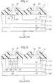
- Fig. 4 is a sectional view illustrating the construction of a bipolar transistor according to another embodiment of the present invention.
- a P + -type region 22 having a smaller width than the base contact region 14 is provided in a middle portion of the base contact region 14.
- a Schottky junction is formed by the base electrode 15 and the P-type base region 12. With this Schottky junction, a Schottky diode is provided in the boundary portion of the base contact region 14.
- minority carriers (electrons) remaining in the base region 12 are speedily released through the Schottky junction. This suppresses the accumulation of the minority carriers in the base region 12 as in the first embodiment, thereby speeding up the switching operation.
- Fig. 5 is a sectional view illustrating the construction of a bipolar transistor according to further another embodiment of the present invention.
- parts corresponding to those shown in Fig. 1 are denoted by the same reference characters as in Fig. 1.
- an N + -type region 23 having a small width is provided in the boundary portion of the base contact region 14 to surround the base contact region 14.
- P + -type regions 24 and an N + -type region 25 each having a small width are alternately provided in a region surrounded by the N + -type region 23. That is, a universal contact structure is provided in the base contact region 14.
- the present invention may be embodies in any other forms.
- the contact region 14 having a generally C-shape as viewed in plan is provided in the embodiments described above, the base contact region 14 may have a ring shape as shown in Fig. 6 to surround the emitter region 13.
- the N-type region 21 and the N + -type region 23 are not necessarily required to be each provided in the entire boundary portion of the base contact region 14.
- the N-type region 21 and the N + -type region 23 may each be provided only in a part closer to the bonding region 26, but not in a part relatively remote from the bonding region 26.
- the N-type region 21 and the N + -type region 23 may each be provided only in a part of the boundary portion of the base contact region 14 closer to the emitter region 13.
- the present invention is applicable to a PNP-type bipolar transistor.
- a P-type region or a P + -type region having the same conductivity type as the emitter region is provided in the boundary portion of the base contact region defined in the N-type base region, or a P + -type region having a smaller width than the base contact region is provided in the middle portion of the base contact region.
- the present invention is applicable to a semiconductor device having a plurality of bipolar transistors. Further, the invention is applicable to a semiconductor device including a functional element other than the bipolar transistor, such as a thyristor, triac or a GTO (gate turn-off thyristor), which has a PN junction.
- a functional element other than the bipolar transistor such as a thyristor, triac or a GTO (gate turn-off thyristor), which has a PN junction.
Landscapes
- Bipolar Transistors (AREA)
- Electrodes Of Semiconductors (AREA)
- Thyristors (AREA)
Abstract
Description
Claims (10)
- A semiconductor device comprising:wherein a diode is provided in a boundary portion of a contact region to which an electrode is connected in the first conductivity type semiconductor region.a functional element having a first conductivity type semiconductor region provided in a semiconductor substrate, and a second conductivity type semiconductor region provided in contact with the first conductivity type semiconductor region and having a conductivity type different from that of the first conductivity type semiconductor region,
- A semiconductor device as set forth in claim 1, wherein the diode is a PN diode constituted by the first conductivity type semiconductor region and a second conductivity type region embedded in the first conductivity type semiconductor region in contact with a boundary of the contact region and having a conductivity type different from that of the first conductivity type semiconductor region.
- A semiconductor device as set forth in claim 2, wherein a universal contact structure is provided in the contact region with the second conductivity type region in contact with the boundary portion of the contact region.
- A semiconductor device as set forth in claim 1,
wherein a high-concentration impurity region having the same conductivity type as the first conductivity type semiconductor region and a higher impurity concentration than the first conductivity type semiconductor region is provided in contact with the electrode in the contact region,
wherein the diode is a Schottky diode having a Schottky junction formed by the electrode connected to the contact region and the first conductivity type semiconductor region. - A semiconductor device as set forth in any of claims 1 to 4, wherein the diode is provided adjacent a surface of the first conductivity type semiconductor region.
- A semiconductor device as set forth in any of claims 1 to 5, wherein the contact region has a generally C-shape or a ring shape which surrounds the second conductivity type semiconductor region on the surface of the first conductivity type semiconductor region.
- A semiconductor device as set forth in any of claims 1 to 6, wherein the diode is provided at least in a part of the boundary portion of the contact region facing the second conductivity type semiconductor region.
- A semiconductor device as set forth in any of claims 1 to 6, wherein the diode is provided in the entire boundary portion of the contact region.
- A semiconductor device as set forth in any of claims 1 to 7, wherein a bonding region is defined on the first conductivity type semiconductor region for bonding a wire to the electrode, and the diode is provided at least in a part of the boundary portion of the contact region adjacent to the bonding region.
- A semiconductor device as set forth in any of claims 1 to 9, wherein the functional element is a bipolar transistor which comprises a base region defined by the first conductivity type semiconductor region, and an emitter region defined by the second conductivity type semiconductor region.
Applications Claiming Priority (3)
| Application Number | Priority Date | Filing Date | Title |
|---|---|---|---|
| JP25588199A JP4707203B2 (en) | 1999-09-09 | 1999-09-09 | Semiconductor device |
| JP25588199 | 1999-09-09 | ||
| PCT/JP2000/006035 WO2001020683A1 (en) | 1999-09-09 | 2000-09-06 | Semiconductor device |
Publications (2)
| Publication Number | Publication Date |
|---|---|
| EP1211733A1 true EP1211733A1 (en) | 2002-06-05 |
| EP1211733A4 EP1211733A4 (en) | 2007-01-17 |
Family
ID=17284869
Family Applications (1)
| Application Number | Title | Priority Date | Filing Date |
|---|---|---|---|
| EP00956947A Withdrawn EP1211733A4 (en) | 1999-09-09 | 2000-09-06 | SEMICONDUCTOR DEVICE |
Country Status (5)
| Country | Link |
|---|---|
| US (1) | US6897546B1 (en) |
| EP (1) | EP1211733A4 (en) |
| JP (1) | JP4707203B2 (en) |
| TW (1) | TW479361B (en) |
| WO (1) | WO2001020683A1 (en) |
Cited By (2)
| Publication number | Priority date | Publication date | Assignee | Title |
|---|---|---|---|---|
| EP1429390A3 (en) * | 2002-12-09 | 2005-11-09 | Micrel, Inc. | Bipolar junction transistor |
| EP2693463A4 (en) * | 2011-03-28 | 2014-09-17 | Nat Inst Of Advanced Ind Scien | SEMICONDUCTOR DEVICE HAVING AMPLIFYING FACTOR WITH DEPENDENCE ON CURRENT VALUE |
Families Citing this family (2)
| Publication number | Priority date | Publication date | Assignee | Title |
|---|---|---|---|---|
| JP2010034312A (en) * | 2008-07-29 | 2010-02-12 | Rohm Co Ltd | Semiconductor device and manufacturing method therefor |
| FR3036001A1 (en) * | 2015-05-05 | 2016-11-11 | St Microelectronics Tours Sas | BIDIRECTIONAL POWER SWITCH |
Family Cites Families (15)
| Publication number | Priority date | Publication date | Assignee | Title |
|---|---|---|---|---|
| US3858234A (en) * | 1973-01-08 | 1974-12-31 | Motorola Inc | Transistor having improved safe operating area |
| JPS5858361U (en) * | 1981-10-16 | 1983-04-20 | オリジン電気株式会社 | semiconductor equipment |
| JPS5866356A (en) * | 1981-10-16 | 1983-04-20 | Origin Electric Co Ltd | Controllable semiconductor device |
| JPS61166170A (en) * | 1985-01-18 | 1986-07-26 | Matsushita Electronics Corp | Semiconductor integrated circuit |
| JPS628565A (en) * | 1985-07-04 | 1987-01-16 | Nec Corp | semiconductor equipment |
| JPS6258678A (en) * | 1985-09-06 | 1987-03-14 | Matsushita Electronics Corp | transistor |
| US4933740A (en) * | 1986-11-26 | 1990-06-12 | General Electric Company | Insulated gate transistor with vertical integral diode and method of fabrication |
| US4871686A (en) * | 1988-03-28 | 1989-10-03 | Motorola, Inc. | Integrated Schottky diode and transistor |
| JPH01169048U (en) * | 1988-05-19 | 1989-11-29 | ||
| JPH02222541A (en) * | 1989-02-23 | 1990-09-05 | Nec Corp | bipolar transistor |
| JPH04275432A (en) * | 1991-03-04 | 1992-10-01 | Matsushita Electron Corp | Semiconductor device |
| JP2503130B2 (en) * | 1991-07-29 | 1996-06-05 | 信越半導体株式会社 | Liquid phase growth method |
| DE4405815A1 (en) | 1993-02-24 | 1994-08-25 | Samsung Electronics Co Ltd | Semiconductor device having an anode layer which has low-concentration regions formed by selective diffusion |
| JP3155134B2 (en) * | 1993-10-27 | 2001-04-09 | ローム株式会社 | Semiconductor device |
| EP0720237A1 (en) * | 1994-12-30 | 1996-07-03 | STMicroelectronics S.r.l. | Zener diode for integrated circuits |
-
1999
- 1999-09-09 JP JP25588199A patent/JP4707203B2/en not_active Expired - Lifetime
-
2000
- 2000-09-06 WO PCT/JP2000/006035 patent/WO2001020683A1/en not_active Ceased
- 2000-09-06 US US10/070,536 patent/US6897546B1/en not_active Expired - Lifetime
- 2000-09-06 EP EP00956947A patent/EP1211733A4/en not_active Withdrawn
- 2000-09-08 TW TW089118445A patent/TW479361B/en not_active IP Right Cessation
Cited By (4)
| Publication number | Priority date | Publication date | Assignee | Title |
|---|---|---|---|---|
| EP1429390A3 (en) * | 2002-12-09 | 2005-11-09 | Micrel, Inc. | Bipolar junction transistor |
| US7145206B2 (en) | 2002-12-09 | 2006-12-05 | Micrel, Inc. | MOS field effect transistor with reduced parasitic substrate conduction |
| EP2693463A4 (en) * | 2011-03-28 | 2014-09-17 | Nat Inst Of Advanced Ind Scien | SEMICONDUCTOR DEVICE HAVING AMPLIFYING FACTOR WITH DEPENDENCE ON CURRENT VALUE |
| US8921213B2 (en) | 2011-03-28 | 2014-12-30 | National Institute Of Advanced Industrial Science And Technology | Method of making less electric current dependence of electric current gain of semiconductor device |
Also Published As
| Publication number | Publication date |
|---|---|
| JP2001085443A (en) | 2001-03-30 |
| EP1211733A4 (en) | 2007-01-17 |
| US6897546B1 (en) | 2005-05-24 |
| WO2001020683A1 (en) | 2001-03-22 |
| JP4707203B2 (en) | 2011-06-22 |
| TW479361B (en) | 2002-03-11 |
Similar Documents
| Publication | Publication Date | Title |
|---|---|---|
| JP3949251B2 (en) | ESD protection circuit | |
| CN102017162B (en) | Integrated low leakage schottky diode | |
| JP2525208B2 (en) | Integrated device | |
| US5545917A (en) | Separate protective transistor | |
| JP4017258B2 (en) | Semiconductor device | |
| JPH04233232A (en) | Semiconductor device | |
| JP2862027B2 (en) | Insulated gate bipolar transistor | |
| JPH07297373A (en) | Integrated driver circuit device for inductive load elements | |
| US4982245A (en) | Compound diode assembly of reduced leakage current | |
| SE431381B (en) | DOUBLE FLOOD PROTECTION | |
| JP2970774B2 (en) | Semiconductor device | |
| US5514901A (en) | Epitaxial island with adjacent asymmetrical structure to reduce collection of injected current from the island into other islands | |
| US6897546B1 (en) | Semiconductor device including a functional element having a PN junction | |
| EP0341730A2 (en) | Gate-controlled bidirectional semiconductor switching device | |
| JP2003060059A (en) | Protective circuit and protective element | |
| JPH0465552B2 (en) | ||
| US10325905B2 (en) | Semiconductor device and semiconductor circuit device | |
| JP3459532B2 (en) | Semiconductor integrated circuit and method of manufacturing the same | |
| US6144066A (en) | Protection of the logic well of a component including an integrated MOS power transistor | |
| CN116805625A (en) | Overvoltage protection device with trench contacts | |
| JP3216315B2 (en) | Insulated gate bipolar transistor | |
| JPH08102536A (en) | Insulated gate type semiconductor device | |
| JPH09283755A (en) | Semiconductor device | |
| US20240222476A1 (en) | Wide based high voltage bipolar junction transistor with buried collectors as hybrid igbt building block | |
| EP0813247B1 (en) | A separate protective transistor to reduce injected current from one PN-junction-isolated island to another |
Legal Events
| Date | Code | Title | Description |
|---|---|---|---|
| PUAI | Public reference made under article 153(3) epc to a published international application that has entered the european phase |
Free format text: ORIGINAL CODE: 0009012 |
|
| 17P | Request for examination filed |
Effective date: 20020307 |
|
| AK | Designated contracting states |
Kind code of ref document: A1 Designated state(s): AT BE CH CY DE DK ES FI FR GB GR IE IT LI LU MC NL PT SE |
|
| RBV | Designated contracting states (corrected) |
Designated state(s): AT BE CH CY DE FR IT LI NL |
|
| A4 | Supplementary search report drawn up and despatched |
Effective date: 20061214 |
|
| RIC1 | Information provided on ipc code assigned before grant |
Ipc: H01L 29/10 20060101ALI20061208BHEP Ipc: H01L 29/73 20060101AFI20010327BHEP |
|
| 17Q | First examination report despatched |
Effective date: 20070525 |
|
| STAA | Information on the status of an ep patent application or granted ep patent |
Free format text: STATUS: THE APPLICATION IS DEEMED TO BE WITHDRAWN |
|
| 18D | Application deemed to be withdrawn |
Effective date: 20100402 |