EP1211558A1 - Substrate selector - Google Patents
Substrate selector Download PDFInfo
- Publication number
- EP1211558A1 EP1211558A1 EP01934361A EP01934361A EP1211558A1 EP 1211558 A1 EP1211558 A1 EP 1211558A1 EP 01934361 A EP01934361 A EP 01934361A EP 01934361 A EP01934361 A EP 01934361A EP 1211558 A1 EP1211558 A1 EP 1211558A1
- Authority
- EP
- European Patent Office
- Prior art keywords
- substrate
- defect
- defects
- substrates
- results
- Prior art date
- Legal status (The legal status is an assumption and is not a legal conclusion. Google has not performed a legal analysis and makes no representation as to the accuracy of the status listed.)
- Granted
Links
Images


Classifications
-
- G—PHYSICS
- G05—CONTROLLING; REGULATING
- G05B—CONTROL OR REGULATING SYSTEMS IN GENERAL; FUNCTIONAL ELEMENTS OF SUCH SYSTEMS; MONITORING OR TESTING ARRANGEMENTS FOR SUCH SYSTEMS OR ELEMENTS
- G05B19/00—Programme-control systems
- G05B19/02—Programme-control systems electric
- G05B19/418—Total factory control, i.e. centrally controlling a plurality of machines, e.g. direct or distributed numerical control [DNC], flexible manufacturing systems [FMS], integrated manufacturing systems [IMS], computer integrated manufacturing [CIM]
- G05B19/41875—Total factory control, i.e. centrally controlling a plurality of machines, e.g. direct or distributed numerical control [DNC], flexible manufacturing systems [FMS], integrated manufacturing systems [IMS], computer integrated manufacturing [CIM] characterised by quality surveillance of production
-
- G—PHYSICS
- G03—PHOTOGRAPHY; CINEMATOGRAPHY; ANALOGOUS TECHNIQUES USING WAVES OTHER THAN OPTICAL WAVES; ELECTROGRAPHY; HOLOGRAPHY
- G03F—PHOTOMECHANICAL PRODUCTION OF TEXTURED OR PATTERNED SURFACES, e.g. FOR PRINTING, FOR PROCESSING OF SEMICONDUCTOR DEVICES; MATERIALS THEREFOR; ORIGINALS THEREFOR; APPARATUS SPECIALLY ADAPTED THEREFOR
- G03F1/00—Originals for photomechanical production of textured or patterned surfaces, e.g., masks, photo-masks, reticles; Mask blanks or pellicles therefor; Containers specially adapted therefor; Preparation thereof
- G03F1/68—Preparation processes not covered by groups G03F1/20 - G03F1/50
- G03F1/82—Auxiliary processes, e.g. cleaning or inspecting
- G03F1/84—Inspecting
-
- G—PHYSICS
- G05—CONTROLLING; REGULATING
- G05B—CONTROL OR REGULATING SYSTEMS IN GENERAL; FUNCTIONAL ELEMENTS OF SUCH SYSTEMS; MONITORING OR TESTING ARRANGEMENTS FOR SUCH SYSTEMS OR ELEMENTS
- G05B2219/00—Program-control systems
- G05B2219/30—Nc systems
- G05B2219/32—Operator till task planning
- G05B2219/32186—Teaching inspection data, pictures and criteria and apply them for inspection
-
- G—PHYSICS
- G05—CONTROLLING; REGULATING
- G05B—CONTROL OR REGULATING SYSTEMS IN GENERAL; FUNCTIONAL ELEMENTS OF SUCH SYSTEMS; MONITORING OR TESTING ARRANGEMENTS FOR SUCH SYSTEMS OR ELEMENTS
- G05B2219/00—Program-control systems
- G05B2219/30—Nc systems
- G05B2219/32—Operator till task planning
- G05B2219/32201—Build statistical model of past normal proces, compare with actual process
-
- Y—GENERAL TAGGING OF NEW TECHNOLOGICAL DEVELOPMENTS; GENERAL TAGGING OF CROSS-SECTIONAL TECHNOLOGIES SPANNING OVER SEVERAL SECTIONS OF THE IPC; TECHNICAL SUBJECTS COVERED BY FORMER USPC CROSS-REFERENCE ART COLLECTIONS [XRACs] AND DIGESTS
- Y02—TECHNOLOGIES OR APPLICATIONS FOR MITIGATION OR ADAPTATION AGAINST CLIMATE CHANGE
- Y02P—CLIMATE CHANGE MITIGATION TECHNOLOGIES IN THE PRODUCTION OR PROCESSING OF GOODS
- Y02P90/00—Enabling technologies with a potential contribution to greenhouse gas [GHG] emissions mitigation
- Y02P90/02—Total factory control, e.g. smart factories, flexible manufacturing systems [FMS] or integrated manufacturing systems [IMS]
Definitions
- the present invention relates to substrate-selecting equipment for a photomask used for the production of semiconductor integrated circuit and in particular to substrate-selecting equipment for selecting a substrate used for an objective product from among a group of substrates with photosensitive material layer used for the production of photomasks.
- substrate (it is called “blanks”) provided with shielding film or shifter layer 820 made of metallic thin film such as chromium formed on a transparent substrate 810 by sputtering and others is provided.
- shielding film or shifter layer 820 made of metallic thin film such as chromium formed on a transparent substrate 810 by sputtering and others is provided.
- photosensitive material layer (it is called "photosensitive resin film, photosensitive resist or merely resist”) 830 is laminated on shielding film or shifter layer 820, and then dried by heating to remove solvent remaining in the photosensitive material layer and improve the adhesion between the metallic thin film and the transparent substrate.
- ionizing radiation 840 such as EB (Electron Beam), laser beam, X-ray is applied so as to selectively expose the ionizing radiation into a desired pattern.
- ionizing radiation 840 is selectively exposed by means of the fixed equipment according to pattern data for the formation of pattern. Therefore, it is also called “pattern writing” or merely "writing”.
- Fig. 8(d) photosensitive material layer 830 is developed to form resist pattern 835.
- Fig. 8(e) areas of the shielding layer 820 made of metallic thin film bared from openings 836 of resist pattern 835 are etched so that shielding layer pattern 825 is formed.
- resist pattern 835 is removed so that a photomask with shielding layer pattern 825 can be obtained as shown in Fig. 8(f). Thereafter, inspection is carried out and correction of pattern is carried out according to demand so that a desired photomask is obtained.
- circuits of semiconductor products such as LSI chips are becoming dense and minute higher and higher, the formation of patterns having higher accuracy and higher quality have come to be desired.
- the present invention is a substrate-selecting equipment for selecting substrates used for objective products from among a group of substrates with photosensitive material layers used for the production of photomask, wherein the substrate-selecting equipment comprises one or more of the defect registering part(s) for registering the results of the inspection of defects of substrates with photosensitive material layers in database, the photosensitive material layer lot check result registering part for registering the results of check of lots of photosensitive material layers in database and the substrate-selecting part for selecting substrates used for the production of objective products from among a group of substrates with photosensitive material layers, on the basis of the results of inspection of defects and the results of check of lots of photosensitive materials registered in database.
- the substrate-selecting equipment comprises one or more of the defect registering part(s) for registering the results of the inspection of defects of substrates with photosensitive material layers in database, the photosensitive material layer lot check result registering part for registering the results of check of lots of photosensitive material layers in database and the substrate-selecting part for
- the defect registering part is comprised of the pinhole defect registering part for registering the results of inspection of pinhole defects of blanks in which photosensitive material layers are not laminated on substrates in database and the foreign substance defect registering part for registering the results of inspection of foreign substance in database.
- the above-mentioned substrate-selecting equipment further comprises the selection standard registering part for registering the quality standard of substrates which is the standard of selection of substrates in database, wherein the substrate selection part selects substrates used for the production of objective products, on the basis of the information on the results of check of lots of photosensitive material layers and the quality standard of substrates which is the standard of the selection of substrates, according to demand.
- the above-mentioned substrate-selecting equipment further comprises the in pattern area existing defect extracting part for extracting defects existing in a pattern area on a photomask wherein defects existing in a pattern area on a photomask are extracted corresponding with the pattern area of photomask produced every substrate, on the basis of the information on the results of inspection of defects of each substrate and the information on the results of check of lots of photosensitive material layers registered in database, for candidate substrate nominated for a candidate of substrate used for photomask to be produced.
- the above-mentioned substrate-selecting equipment further comprises the defect probability calculating part for calculating the probability that no defect happens s or the probability that happen in the surrounding part of a pattern of photomask produced or for calculating the probability that no defect happens s or the probability that defects happen inside a pattern of photomask produced, corresponding with the patterns of photomask produced every substrate, on the basis of the information on the results of inspection of defects of each substrate and the information on the results of check of lots of photosensitive material layers registered in a database for candidate substrate nominated for candidate of substrate used for photomask to be produced, and wherein the substrate-selecting part selects substrates used for the production of objective products, on the basis of the probability that no defect happens s or the probability that defects happen in the surrounding part of pattern every substrate obtained in the defect probability calculating part, or from the probability that no defect happens or the probability that defects happen over the whole of pattern, according to demand.
- the defect probability calculating part for calculating the probability that no defect happens s or the probability that happen in
- defect areas having the size larger than the size of defects decided considering errors, corresponding to the position of defect on photomask to be produced, are obtained for all the defects in a substrate, and the non-occurrence probabilities that no defect happens in the surrounding part of patterns in the obtained defect areas are obtained for all the defects in a substrate.
- product of non-occurrence probabilities for all the defects in a substrate are obtained, wherein the above-mentioned product corresponds to the probability P0 that no defect happens in the surrounding part of patterns on a photomask on a substrate.
- defect areas having the size larger than the size of defects decided considering errors, corresponding to the position of defect on photomask to be produced, are obtained for all the defects in a substrate, and the non-occurrence probabilities that no defect happens inside patterns in the obtained defect area are obtained for all the defects in a substrate.
- product of non-occurrence probabilities for all the defects in a substrate are obtained, wherein the above-mentioned product corresponds to the probability P01 that no defect happens over the whole of patterns on a photomask on a substrate.
- the above-mentioned probability includes (approximate) probabilities having substantially meanings, which probabilities are calculated by approximate calculation.
- ionizing radiation 840 such as EB (Electron Beam), laser beam, X-ray is applied to photosensitive material layer 830 of substrate with photosensitive material layer so as to selectively expose the photosensitive material layer to the ionizing radiation into a desired pattern by which latent image thereof is formed.
- ionizing radiation 840 is selectively exposed by means of the fixed equipment according to pattern data for the formation of pattern. Therefore, it is also called “pattern writing” or merely “writing” and a pattern area on a photomask is also called “writing area”.
- the substrate-selecting equipment of the present invention having the above-mentioned constitution enables the provision of the substrate-selecting equipment in which substrates used for the provision of objective products can be successfully selected from among a group of substrates with photosensitive material layers employed for writing of pattern in the provision of photomask, particularly from the phase of quality of product.
- the substrate-selecting equipment for selecting substrates used for objective parts from among a group of substrates with photosensitive material layers used for the production of photomask, wherein the substrate-selecting equipment comprises one or more of the defect registering part(s) for registering the results of the inspection of defects of substrates with photosensitive material layers in database, the photosensitive material layer lot check result registering part and the substrate-selecting part for selecting substrates used for the production of objective products from among a group of a group of substrates with photosensitive material layer on the basis of the results of inspection of defects and the results of check of lots of photosensitive material layers registered in database.
- the above-mentioned substrate-selecting equipment further comprises the selection standard registering part for registering the quality standard (it is called also "rank") of substrates which is the standard of selection of substrates in database, wherein the substrate selection part can select substrates used for the production of objective products on the basis of the information on the results of check of lots of photosensitive material layers and the quality standard of substrates which is the standard of the selection of substrates, according to demand.
- the selection standard registering part for registering the quality standard (it is called also "rank") of substrates which is the standard of selection of substrates in database
- the substrate selection part can select substrates used for the production of objective products on the basis of the information on the results of check of lots of photosensitive material layers and the quality standard of substrates which is the standard of the selection of substrates, according to demand.
- the above-mentioned substrate-selecting equipment further comprises the defect probability calculating part wherein the probability that no defect happens s or the probability that happen in the surrounding part of a patterns on photomask produced is extracted corresponding with the patterns of photomask to be produced every substrate, on the basis of the information of the results of inspection of defects of each substrate and the information on the results of check of the lot of photosensitive material layers registered in a database for candidate substrate nominated for candidate of substrate used for photomask to be produced, and wherein the substrate-selecting part can select substrates used for the production of objective products on the basis of the probability that no defect happens or the probability that defects happen in the surrounding part of pattern every substrate obtained in the defect probability calculating part, or from the probability that no defect happens or the probability that defects happen in the whole of pattern, according to demand.
- Fig. 1 the substrate-selecting equipment and the step of the selection of substrate (S150) are shown inside the area bounded by the dotted line shows. Further, steps of S110 to S170 shown in Fig. 1 and steps of S510 to S540 shown in Fig. 6 are steps of processing.
- numeral 110 designates the pinhole defect inspection result registering part for registering the results of inspection of pinhole defects
- numeral 120 designates the foreign substance defect inspection result registering part for registering the results of inspection of foreign substance defects
- numeral 130 designates the photosensitive material layer lot checking result registering part for registering the results of check of lots of photosensitive material layers
- numeral 140 designates the selection standard registering part for registering the standard of selection of substrate
- numeral 150 designates the substrate-selecting part for selecting substrate
- numeral 151 designates the in pattern area happening defect extracting part for extracting defects which happen within a pattern area
- numeral 152 designates the defect probability calculating part for calculating the probability that defects will happen
- numeral 160 designates database
- numeral 171 designates writing pattern
- numeral 172 designates the information on arrangement
- numeral 181 designates data on the results of inspection of pinhole defects
- numeral 182 designates data on the results of inspection of foreign substance defects
- numeral 183 designates data on the results of
- An example of mode of working of substrate-selecting equipment of the present invention is a substrate-selecting equipment for selecting substrate qualitatively corresponding to an objective product from among a group of substrates provided with photosensitive material layer used for producing a photomask, wherein the selected substrate is provided for step of writing of pattern.
- a substrate-selecting equipment of the present example comprises the pinhole defect inspection results registering part 110 for registering the results of inspection of pinhole defects (data 181 on the results of inspection of pinhole defects) in database 160, the foreign substance defect inspection result registering part 120 for registering the results of inspection of foreign substance defects existing in a substrate provided with photosensitive material layers (data 182 on the results of inspection of foreign substance defects) in database 160, the photosensitive material layer lot checking result registering part 130 for registering the results of check of sensitivity of lots of photosensitive material layers every lot of photosensitive material layers(data 183 on the results of check of inspection of sensitivity of photosensitive material layer every lot of photosensitive material layers) in database 160, the selection standard registering part 140 for registering the quality standard (the specification 184 of photomask) which is the standard of selection of substrate in database 160 and the substrate-selecting part 150 for selecting a substrate used for the production of objective products which are suitable qualitatively, on the basis of the results of inspection of defects registered in database
- inspection of pinhole defects is carried out by means of the fixed pinhole inspection equipment for blanks in which shielding layer or shifter layer made of thin film of metal such as chromium is laminated on a transparent substrate made of, for example, quartz blanks.
- the results of inspection are stored as data 181 on the results of inspection of pinhole defects, sent through the pinhole defects inspection result registering part 110 to database 160 and restored in the database 160.
- the blanks are cleaned and photosensitive material is applied on the blanks so that photosensitive material layer is formed, wherein after forming of photosensitive material layer, the inspection (S120) of foreign substance defects is carried out by means of a fixed inspection equipment.
- the results of inspection are stored as data 182 on the results of inspection of foreign substance defects. Further, the results of inspection is sent through the foreign substance defect inspection result registering part 120 to database 160, and stored in the database 160.
- a check (S130) of sensitivity of photosensitive material layer is carried out using test pieces (substrates for test) every lot of photosensitive material layers, wherein the results of inspection are stored as data 183 on a check of the sensitivity of lots of sensitive material layer, sent through the photosensitive material layer sensitivity lot check result registering part 130 to database 160, and stored in database 160.
- the selection (S150) of substrate for selecting the objective substrate from among a group of substrates provided with photosensitive material layer is carried out by means of the equipment of the present example, wherein selection (S160) of a substrate for writing is carried out and writing (S170) of pattern on the substrate is carried out by means of a writer.
- Data of inspection of defects such as data 181 on the results of inspection of pinhole defects or data 182 on the results of inspection of foreign substance defects are caught on size and position (the expression in coordinates of X-Y of defect of individual substrate detected by the inspection of defects. They are shown, for example, as shown in Fig. 2.
- the sensitivity of individual application lots of photosensitive materials (wherein the lots differs according to the date of application), is detected for individual test piece, and exposure amount (irradiation amount) corresponding to a writer is determined.
- the size of substrate, a kind of shielding film, a kind of photosensitive material layer, the date of application, a writer and exposure amount of individual substrate are correspondent to each other, wherein the data 183 is expressed as shown in Fig. 3.
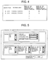
- Fig. 4 shows an example of the quality standard of as the standard of substrate employed for writing by means of the raster type of electron beam writer, wherein the description written on the first line in a table means that pattern area is 10000 ⁇ m ⁇ 10000 ⁇ m, rank of the results of inspection of pinhole defects is "A” and rank of the results of inspection of foreign substance defects is "B" in case of 0.25 ⁇ m address unit writing.
- selection indication input 190 in case of selecting substrate corresponding to an objective product is carried out selecting quality conditions such as substrate of a writer, the size of substrate and a kind of shielding film a kind of photosensitive material layer and quality conditions such as design rule, rank of the result of inspection of pinhole defects, respectively.
- a substrate is selected according to the information on the defects of inspection of defects, the information on the results of check of lots of photosensitive material layers and the quality standard of substrate being the standard of the selection of substrate, wherein the number of defects existing inside a pattern area of individual photomask to be produced is extracted for individual objective substrate according to the information on the results of inspection of defects registered in database in the in pattern area existing defect extracting part 151 of the substrate-selecting part 150.
- the rank is given to each objective substrate according to the number of defects extracted so that a desired substrate correspondent to the quality standard of substrate is used.
- the selection of objective substrate of from among substrates in stock is carried out, wherein objective substrates 523 correspondent to the conditions 512 of employment of substrate such as a writer, the size of substrate, a kind of shielding film and a kind of photosensitive material layer, designated by the selection indication input 190 are selected (S510).
- a substrate with a fixed pattern area (an objective substrate 531) is selected from among the objective substrates 523 referring to data 521 on the results of inspection of pinhole defects and data 522 on the results of inspection of foreign substance defects.
- the number of defects existing in pattern area is grasped for a fixed pattern area and for pattern area turned by 90° against the fixed pattern area, respectively (S520).
- Substrates in the desired ranks of substrate are selected from among the objective substrates 531 according to the quality standard (rank of substrate) 532, and substrates are classified into ranks with giving the order of priority (S530) by which the objective substrates 541 with rank and the order of priority can be obtained (540).
- rank is given to the objective substrate 541 of objective product and further the order of priority is given thereto, wherein a desired substrate corresponding to the specification of quality of objective product is selected from among the objective substrates 541 so that the selected substrates are introduced to a writer.
- the second example is explained in which substrates qualitatively corresponding to the objective products are selected in the substrate-selecting part 150.
- substrates are selected on the basis of the information on the results of inspection of defects and the information on the results of check of lots of photosensitive material layer, wherein probability P0 that no defect happens on individual photomask is obtained on the basis of the information on the results of inspection of defects registered in database. Then, the objective substrates are classified into ranks according to the probability P0, by which substrates in a desired rank are selected to provide substrate for the production of photomask.
- probability P0 being obtained, the same calculation of probability is carried out for a fixed pattern area and for pattern area turned by 90° relatively against the fixed pattern area of objective substrates so that probability P0 is obtained for the respective relative angle. Then, the objective substrates are classified including the probability P0 in the respective relative angle by which substrate with a desired rank is selected.
- the objective substrates can be employed more effectively as compared with the first example.
- probabilities that defects cover the circumference of pattern inside a pattern data area are calculated for individual defects 611, 612, 613.
- Probabilities P1, P2, P3 that no defect covers the circumference of pattern inside a pattern data area are calculated from the probabilities that defects cover the circumference of pattern inside a pattern data area, respectively.
- the relation of position between objective substrates, pattern area, pattern data area, and patterns inside the pattern data area is determined according to writing pattern 171 and the information on arrangement 172.
- defect area 621 having the size larger than defect 611 considering errors and corresponding to the position of defect 611 on photomask produced is obtained and the non-occurrence probability that no defect happens in the circumference of pattern inside the obtained defect area 621 is obtained.
- Patterns existing inside defect area 621 (the size of L ⁇ L) with the size larger than defect 611 considering errors shown in Fig. 7(a) is patterns 651, 652 as shown as an enlarged view in Fig. 7(b), wherein the defect area 621 is a rectangular area with the length L of one side.
- defect 611 covers a circumference of patterns in a pattern data area is approximated by (S1 ⁇ d)/(L ⁇ L).
- the probabilities P2, P3 that defects 612, 613 cover circumferences of patterns in a pattern data area can be calculated, respectively.
- the probability P0 that no defect happens on a photomask can be obtained from the obtained probabilities P1, P2 and P3.
- the probability P0 that no defect happens on a photomask can be also calculated basically in the same way.
- a method of calculating the probability P0 in the second example is a method of calculation wherein occurrence of defects included in the inside patterns are not regarded as occurrence of defects, because in case of defects 611, 612 and 613 being included in the inside of patterns, correction of defects can be comparatively easily carried out so that it is made the requisite condition that the defects are corrected practically in the latter work.
- the probability that defects happen can be calculated assuming the defects to happen.
- the probability that circular defect 611 with diameter d strides patterns in a pattern data area can be calculated as Sd/(L ⁇ L), wherein Sd designates the sum of areas of patterns 651, 652 which are thickened outward by d/2.
- the probabilities P12, P13 that defects 612, 613 does not stride patterns in a pattern data area can be obtained.
- the probability P01 that no defect happens on a photomask can be obtained from the obtained probabilities P11, P12 and P13, including a case where defects exist inside patterns.
- the present invention made possible to provide a substrate-selecting equipment in which substrates for producing an objective products can be selected, particularly from the phase of quality of products, from among a group of substrates with photosensitive material layers for forming photomasks with photosensitive material layers, employed for writing of patterns.
- the total productivity of production of photomasks can be improved as compared with conventional case.
- the present invention can cope with the higher precision and the higher quality of photomasks.
Abstract
Description
- The present invention relates to substrate-selecting equipment for a photomask used for the production of semiconductor integrated circuit and in particular to substrate-selecting equipment for selecting a substrate used for an objective product from among a group of substrates with photosensitive material layer used for the production of photomasks.
- In recent years, high-integration and high-function comes to be desired more and more for various LSI typified by ASIC, from the tendency of an electric equipment becoming high-efficient and lighter, thinner, shorter and smaller. In a photomask used for the production of semiconductor integrated circuit, the forming of patterns of photomask with high efficiency and high quality has come to be desired.
- Heretofore, the production of photomask is carried out generally through steps shown in Fig. 8.
- First, as shown in Fig 8(a), substrate (it is called "blanks") provided with shielding film or
shifter layer 820 made of metallic thin film such as chromium formed on atransparent substrate 810 by sputtering and others is provided. - Then, as shown in Fig. 8(b), photosensitive material layer (it is called "photosensitive resin film, photosensitive resist or merely resist") 830 is laminated on shielding film or
shifter layer 820, and then dried by heating to remove solvent remaining in the photosensitive material layer and improve the adhesion between the metallic thin film and the transparent substrate. - Then, as shown in Fig. 8(c), ionizing
radiation 840 such as EB (Electron Beam), laser beam, X-ray is applied so as to selectively expose the ionizing radiation into a desired pattern. Generally, theionizing radiation 840 is selectively exposed by means of the fixed equipment according to pattern data for the formation of pattern. Therefore, it is also called "pattern writing" or merely "writing". - Then, as shown in Fig. 8(d),
photosensitive material layer 830 is developed to formresist pattern 835. Thereafter, as shown in Fig. 8(e), areas of theshielding layer 820 made of metallic thin film bared fromopenings 836 ofresist pattern 835 are etched so thatshielding layer pattern 825 is formed. - Finally,
resist pattern 835 is removed so that a photomask withshielding layer pattern 825 can be obtained as shown in Fig. 8(f). Thereafter, inspection is carried out and correction of pattern is carried out according to demand so that a desired photomask is obtained. - It goes without saying that quality of photomask produced in the above-mentioned process is greatly affected by the quality of substrate with photosensitive material layer employed for pattern writing. However, a kind of substrates with photosensitive material layer is many. Theretofore, the control of substrates with photosensitive material layer is difficult. Heretofore, the distinction between good products and poor products is carried out according to the regular standard in the inspection in the process of production so that only good products are employed.
- However, there are the specifications of quality of objective products are various, and substrates with photosensitive material layers distinguished as good products are varied in the phase of quality and the sensitivity of photosensitive material layers. Therefore, heretofore, it does not always say that substrates corresponding to the specifications of objective products were selected. Accordingly, there are cases where the influence of the used substrate on the inspection and correction thereof was considerable.
- Further, as circuits of semiconductor products such as LSI chips are becoming dense and minute higher and higher, the formation of patterns having higher accuracy and higher quality have come to be desired.
- It is an object of the present invention to provide a substrate-selecting equipment wherein substrates used for the production of objective products can be successfully selected from among a group of substrates with photosensitive material layers used for the production of photomasks employed for writing of patterns in the process of photomask, particularly from the phase of quality of products.
- The present invention is a substrate-selecting equipment for selecting substrates used for objective products from among a group of substrates with photosensitive material layers used for the production of photomask, wherein the substrate-selecting equipment comprises one or more of the defect registering part(s) for registering the results of the inspection of defects of substrates with photosensitive material layers in database, the photosensitive material layer lot check result registering part for registering the results of check of lots of photosensitive material layers in database and the substrate-selecting part for selecting substrates used for the production of objective products from among a group of substrates with photosensitive material layers, on the basis of the results of inspection of defects and the results of check of lots of photosensitive materials registered in database.
- Further, in the above-mentioned substrate-selecting equipment, the defect registering part is comprised of the pinhole defect registering part for registering the results of inspection of pinhole defects of blanks in which photosensitive material layers are not laminated on substrates in database and the foreign substance defect registering part for registering the results of inspection of foreign substance in database.
- Furthermore, the above-mentioned substrate-selecting equipment further comprises the selection standard registering part for registering the quality standard of substrates which is the standard of selection of substrates in database, wherein the substrate selection part selects substrates used for the production of objective products, on the basis of the information on the results of check of lots of photosensitive material layers and the quality standard of substrates which is the standard of the selection of substrates, according to demand.
- Further, the above-mentioned substrate-selecting equipment further comprises the in pattern area existing defect extracting part for extracting defects existing in a pattern area on a photomask wherein defects existing in a pattern area on a photomask are extracted corresponding with the pattern area of photomask produced every substrate, on the basis of the information on the results of inspection of defects of each substrate and the information on the results of check of lots of photosensitive material layers registered in database, for candidate substrate nominated for a candidate of substrate used for photomask to be produced.
- Further, the above-mentioned substrate-selecting equipment further comprises the defect probability calculating part for calculating the probability that no defect happens s or the probability that happen in the surrounding part of a pattern of photomask produced or for calculating the probability that no defect happens s or the probability that defects happen inside a pattern of photomask produced, corresponding with the patterns of photomask produced every substrate, on the basis of the information on the results of inspection of defects of each substrate and the information on the results of check of lots of photosensitive material layers registered in a database for candidate substrate nominated for candidate of substrate used for photomask to be produced, and wherein the substrate-selecting part selects substrates used for the production of objective products, on the basis of the probability that no defect happens s or the probability that defects happen in the surrounding part of pattern every substrate obtained in the defect probability calculating part, or from the probability that no defect happens or the probability that defects happen over the whole of pattern, according to demand.
- Further, in the above-mentioned substrate-selecting equipment, in the defect probability calculating part, defect areas having the size larger than the size of defects decided considering errors, corresponding to the position of defect on photomask to be produced, are obtained for all the defects in a substrate, and the non-occurrence probabilities that no defect happens in the surrounding part of patterns in the obtained defect areas are obtained for all the defects in a substrate. Further, the product of non-occurrence probabilities for all the defects in a substrate are obtained, wherein the above-mentioned product corresponds to the probability P0 that no defect happens in the surrounding part of patterns on a photomask on a substrate.
- Or, in the above-mentioned substrate-selecting equipment, in the defect probability calculating part, defect areas having the size larger than the size of defects decided considering errors, corresponding to the position of defect on photomask to be produced, are obtained for all the defects in a substrate, and the non-occurrence probabilities that no defect happens inside patterns in the obtained defect area are obtained for all the defects in a substrate. Further, the product of non-occurrence probabilities for all the defects in a substrate are obtained, wherein the above-mentioned product corresponds to the probability P01 that no defect happens over the whole of patterns on a photomask on a substrate.
- The above-mentioned probability includes (approximate) probabilities having substantially meanings, which probabilities are calculated by approximate calculation.
- Further, patterns on a photomask are formed the steps shown in Fig. 8, wherein ionizing
radiation 840 such as EB (Electron Beam), laser beam, X-ray is applied tophotosensitive material layer 830 of substrate with photosensitive material layer so as to selectively expose the photosensitive material layer to the ionizing radiation into a desired pattern by which latent image thereof is formed. Generally, ionizingradiation 840 is selectively exposed by means of the fixed equipment according to pattern data for the formation of pattern. Therefore, it is also called "pattern writing" or merely "writing" and a pattern area on a photomask is also called "writing area". - The substrate-selecting equipment of the present invention having the above-mentioned constitution enables the provision of the substrate-selecting equipment in which substrates used for the provision of objective products can be successfully selected from among a group of substrates with photosensitive material layers employed for writing of pattern in the provision of photomask, particularly from the phase of quality of product.
- Concretely, this is achieved by the substrate-selecting equipment for selecting substrates used for objective parts from among a group of substrates with photosensitive material layers used for the production of photomask, wherein the substrate-selecting equipment comprises one or more of the defect registering part(s) for registering the results of the inspection of defects of substrates with photosensitive material layers in database, the photosensitive material layer lot check result registering part and the substrate-selecting part for selecting substrates used for the production of objective products from among a group of a group of substrates with photosensitive material layer on the basis of the results of inspection of defects and the results of check of lots of photosensitive material layers registered in database.
- The above-mentioned substrate-selecting equipment further comprises the selection standard registering part for registering the quality standard (it is called also "rank") of substrates which is the standard of selection of substrates in database, wherein the substrate selection part can select substrates used for the production of objective products on the basis of the information on the results of check of lots of photosensitive material layers and the quality standard of substrates which is the standard of the selection of substrates, according to demand.
- Further, the above-mentioned substrate-selecting equipment further comprises the defect probability calculating part wherein the probability that no defect happens s or the probability that happen in the surrounding part of a patterns on photomask produced is extracted corresponding with the patterns of photomask to be produced every substrate, on the basis of the information of the results of inspection of defects of each substrate and the information on the results of check of the lot of photosensitive material layers registered in a database for candidate substrate nominated for candidate of substrate used for photomask to be produced, and wherein the substrate-selecting part can select substrates used for the production of objective products on the basis of the probability that no defect happens or the probability that defects happen in the surrounding part of pattern every substrate obtained in the defect probability calculating part, or from the probability that no defect happens or the probability that defects happen in the whole of pattern, according to demand.
-
- Fig. 1 is a schematic view showing an example of mode of working of a substrate-selecting equipment of the present invention.
- Fig. 2 is a view showing an example of data on the results of inspection of defects.
- Fig. 3 is a view showing an example of data on the results of check of lots of photosensitive layers.
- Fig. 4 is a view showing an example of quality standard.
- Fig. 5 is a view showing an example of a process of inputting the selection of substrate.
- Fig. 6 is a flow diagram showing an example of procedures of the choice of substrate referring to a view of selection of substrate.
- Fig. 7 is a view for explaining an example of the action of a defect probability calculating part.
- Fig. 8 is a view for explaining a process of producing a photomask.
-
- Referring to drawing, an example of mode of working of a substrate-selecting equipment of the present invention is explained. In Fig. 1, the substrate-selecting equipment and the step of the selection of substrate (S150) are shown inside the area bounded by the dotted line shows. Further, steps of S110 to S170 shown in Fig. 1 and steps of S510 to S540 shown in Fig. 6 are steps of processing.
- In Figs. 1, 6 and 7,
numeral 110 designates the pinhole defect inspection result registering part for registering the results of inspection of pinhole defects;numeral 120 designates the foreign substance defect inspection result registering part for registering the results of inspection of foreign substance defects;numeral 130 designates the photosensitive material layer lot checking result registering part for registering the results of check of lots of photosensitive material layers;numeral 140 designates the selection standard registering part for registering the standard of selection of substrate;numeral 150 designates the substrate-selecting part for selecting substrate;numeral 151 designates the in pattern area happening defect extracting part for extracting defects which happen within a pattern area;numeral 152 designates the defect probability calculating part for calculating the probability that defects will happen;numeral 160 designates database;numeral 171 designates writing pattern;numeral 172 designates the information on arrangement;numeral 181 designates data on the results of inspection of pinhole defects;numeral 182 designates data on the results of inspection of foreign substance defects:numeral 183 designates data on the results of a check on the sensitivity of lots of photosensitive material layers;numeral 184 designates the specification of photomask;numeral 190 designates the selection indication input for indicating the selection of substrate;numeral 511 designates substrates in stock;numeral 512 designates the conditions of employment of substrate;numeral 521 designates data on the results of inspection of pinhole defects;numeral 522 designates data on the results of inspection of the defects of foreign substrate;numeral 523 designates objective substrates;numeral 524 designates a pattern area;numeral 531 designates an objective substrate;numeral 532 designates the quality standard (rank of substrate);numeral 541 designates an objective substrate;numeral 601 designates an area of substrate;numeral 605 designates a pattern area (writing area);numerals numerals numerals numerals - An example of mode of working of substrate-selecting equipment of the present invention is a substrate-selecting equipment for selecting substrate qualitatively corresponding to an objective product from among a group of substrates provided with photosensitive material layer used for producing a photomask, wherein the selected substrate is provided for step of writing of pattern.
- Then, as shown in Fig. 1, a substrate-selecting equipment of the present example comprises the pinhole defect inspection
results registering part 110 for registering the results of inspection of pinhole defects (data 181 on the results of inspection of pinhole defects) indatabase 160, the foreign substance defect inspectionresult registering part 120 for registering the results of inspection of foreign substance defects existing in a substrate provided with photosensitive material layers (data 182 on the results of inspection of foreign substance defects) indatabase 160, the photosensitive material layer lot checkingresult registering part 130 for registering the results of check of sensitivity of lots of photosensitive material layers every lot of photosensitive material layers(data 183 on the results of check of inspection of sensitivity of photosensitive material layer every lot of photosensitive material layers) indatabase 160, the selectionstandard registering part 140 for registering the quality standard (thespecification 184 of photomask) which is the standard of selection of substrate indatabase 160 and the substrate-selectingpart 150 for selecting a substrate used for the production of objective products which are suitable qualitatively, on the basis of the results of inspection of defects registered in database 160 (data 181 on the results of inspection of pinhole defects anddata 182 on the results of inspection of foreign substance defects), the results of check of lots of photosensitive materials and the quality standard which is the standard of selection of substrate. - First, referring to Fig. 1, the relation between steps of processing of substrate carried out before writing is carried out on the substrate and individual parts of a substrate-selecting equipment of the present example is briefly explained.
- First, inspection of pinhole defects (S110) is carried out by means of the fixed pinhole inspection equipment for blanks in which shielding layer or shifter layer made of thin film of metal such as chromium is laminated on a transparent substrate made of, for example, quartz blanks. The results of inspection are stored as
data 181 on the results of inspection of pinhole defects, sent through the pinhole defects inspectionresult registering part 110 todatabase 160 and restored in thedatabase 160. - Then, the blanks are cleaned and photosensitive material is applied on the blanks so that photosensitive material layer is formed, wherein after forming of photosensitive material layer, the inspection (S120) of foreign substance defects is carried out by means of a fixed inspection equipment. The results of inspection are stored as
data 182 on the results of inspection of foreign substance defects. Further, the results of inspection is sent through the foreign substance defect inspectionresult registering part 120 todatabase 160, and stored in thedatabase 160. - Further, a check (S130) of sensitivity of photosensitive material layer is carried out using test pieces (substrates for test) every lot of photosensitive material layers, wherein the results of inspection are stored as
data 183 on a check of the sensitivity of lots of sensitive material layer, sent through the photosensitive material layer sensitivity lot checkresult registering part 130 todatabase 160, and stored indatabase 160. - On the other hand, many substrates provided with photosensitive material layer, which have inspected on the sensitivity of photosensitive material layer, are stored in a fixed storage (not shown).
- Then, the selection (S150) of substrate for selecting the objective substrate from among a group of substrates provided with photosensitive material layer is carried out by means of the equipment of the present example, wherein selection (S160) of a substrate for writing is carried out and writing (S170) of pattern on the substrate is carried out by means of a writer.
- Then, the
respective data data 183 on the results of check of the sensitivity of lots of photosensitive material layers and the specification of photomask are explained, and the selection of substrate carried out in the substrate-selectingpart 150 is explained. - Data of inspection of defects such as
data 181 on the results of inspection of pinhole defects ordata 182 on the results of inspection of foreign substance defects are caught on size and position (the expression in coordinates of X-Y of defect of individual substrate detected by the inspection of defects. They are shown, for example, as shown in Fig. 2. - In
data 183 on the results of check of the sensitivity of lots of photosensitive material layers, the sensitivity of individual application lots of photosensitive materials (wherein the lots differs according to the date of application), is detected for individual test piece, and exposure amount (irradiation amount) corresponding to a writer is determined. The size of substrate, a kind of shielding film, a kind of photosensitive material layer, the date of application, a writer and exposure amount of individual substrate are correspondent to each other, wherein thedata 183 is expressed as shown in Fig. 3. - In fig. 3, "+a" indicates to increase exposure amount by +a so that the correction of unevenness of sensitivity between lots of photosensitive material layers is made.
- In the quality standard being the standard of selection of substrate (the specification of photomask 184), design rule, pattern area (the size of X direction and the size of Y direction thereof), rank of the results of inspection of pinhole defects, rank of the results of inspection of foreign substance defects and others are correspondent to each other, wherein the
data 184 is expressed as shown in Fig. 4. - In this case, Fig. 4 shows an example of the quality standard of as the standard of substrate employed for writing by means of the raster type of electron beam writer, wherein the description written on the first line in a table means that pattern area is 10000 µm × 10000 µm, rank of the results of inspection of pinhole defects is "A" and rank of the results of inspection of foreign substance defects is "B" in case of 0.25 µm address unit writing.
- For example, in an input screen (of a display of terminal of computer) shown in Fig. 5, input (corresponding to "
selection indication input 190") in case of selecting substrate corresponding to an objective product is carried out selecting quality conditions such as substrate of a writer, the size of substrate and a kind of shielding film a kind of photosensitive material layer and quality conditions such as design rule, rank of the result of inspection of pinhole defects, respectively. - Referring to Fig. 6, an example of flow (algorithm) of the first example wherein substrate qualitatively corresponding to an objective product is selected in the substrate-selecting
part 150 is explained. - In the first example, a substrate is selected according to the information on the defects of inspection of defects, the information on the results of check of lots of photosensitive material layers and the quality standard of substrate being the standard of the selection of substrate, wherein the number of defects existing inside a pattern area of individual photomask to be produced is extracted for individual objective substrate according to the information on the results of inspection of defects registered in database in the in pattern area existing
defect extracting part 151 of the substrate-selectingpart 150. The rank is given to each objective substrate according to the number of defects extracted so that a desired substrate correspondent to the quality standard of substrate is used. - First, the selection of objective substrate of from among substrates in stock is carried out, wherein
objective substrates 523 correspondent to theconditions 512 of employment of substrate such as a writer, the size of substrate, a kind of shielding film and a kind of photosensitive material layer, designated by theselection indication input 190 are selected (S510). - Then, a substrate with a fixed pattern area (an objective substrate 531) is selected from among the
objective substrates 523 referring todata 521 on the results of inspection of pinhole defects anddata 522 on the results of inspection of foreign substance defects. The number of defects existing in pattern area is grasped for a fixed pattern area and for pattern area turned by 90° against the fixed pattern area, respectively (S520). - There is a case where the number of defects existing in a fixed pattern area changes by turning pattern area by 90°.
- Substrates in the desired ranks of substrate are selected from among the
objective substrates 531 according to the quality standard (rank of substrate) 532, and substrates are classified into ranks with giving the order of priority (S530) by which theobjective substrates 541 with rank and the order of priority can be obtained (540). - In such a way, rank is given to the
objective substrate 541 of objective product and further the order of priority is given thereto, wherein a desired substrate corresponding to the specification of quality of objective product is selected from among theobjective substrates 541 so that the selected substrates are introduced to a writer. - The second example is explained in which substrates qualitatively corresponding to the objective products are selected in the substrate-selecting
part 150. - In the second example, substrates are selected on the basis of the information on the results of inspection of defects and the information on the results of check of lots of photosensitive material layer, wherein probability P0 that no defect happens on individual photomask is obtained on the basis of the information on the results of inspection of defects registered in database. Then, the objective substrates are classified into ranks according to the probability P0, by which substrates in a desired rank are selected to provide substrate for the production of photomask.
- In case of probability P0 being obtained, the same calculation of probability is carried out for a fixed pattern area and for pattern area turned by 90° relatively against the fixed pattern area of objective substrates so that probability P0 is obtained for the respective relative angle. Then, the objective substrates are classified including the probability P0 in the respective relative angle by which substrate with a desired rank is selected.
- In this case, the objective substrates can be employed more effectively as compared with the first example.
- Then, referring to Fig. 7, one example of a method of obtaining probability P0 that no defect happens on photomask in a case where there is the fixed relative relation of position between the objective substrates and pattern areas is explained.
- In order to facilitate the explanation, a method of obtaining probability P0 that no defect happens is explained, for concrete example, on a photomask in which three defects (
defects pattern data areas writing area 605 onsubstrate area 601. - First, probabilities that defects cover the circumference of pattern inside a pattern data area are calculated for
individual defects - In this case, the relation of position between objective substrates, pattern area, pattern data area, and patterns inside the pattern data area is determined according to writing
pattern 171 and the information onarrangement 172. - As for the probability P1 that
defect 611 does not cover the circumference of pattern inside a pattern data area,defect area 621 having the size larger thandefect 611 considering errors and corresponding to the position ofdefect 611 on photomask produced is obtained and the non-occurrence probability that no defect happens in the circumference of pattern inside the obtaineddefect area 621 is obtained. - Patterns existing inside defect area 621 (the size of L × L) with the size larger than
defect 611 considering errors shown in Fig. 7(a) ispatterns defect area 621 is a rectangular area with the length L of one side. - In this case, if defect has a circle with diameter d and the sum total of perimeters of
patterns defect 611 covers a circumference of patterns in a pattern data area is approximated by (S1 × d)/(L × L). - Accordingly, the probability P1 that
defect 611 does not cover a circumference of patterns in a pattern data area can be calculated by P1 = 1 - [(S1 × d)/(L × L)]. - In the same way, the probabilities P2, P3 that
defects - The probability P0 that no defect happens on a photomask can be obtained from the obtained probabilities P1, P2 and P3.
- In a case where there are three pattern areas, the probability P0 that no defect happens on a photomask can be also calculated basically in the same way.
- A method of calculating the probability P0 in the second example is a method of calculation wherein occurrence of defects included in the inside patterns are not regarded as occurrence of defects, because in case of
defects - Of course, also in a case where
defects - In this case, for example, in
defect area 621 as shown in Fig. 7(b), the probability thatcircular defect 611 with diameter d strides patterns in a pattern data area can be calculated as Sd/(L × L), wherein Sd designates the sum of areas ofpatterns - Accordingly, the probability P11 that
defect 611 do not stride patterns in a pattern data area can be obtained as P11 = 1-[Sd/(L × L)]. - In the same manner, the probabilities P12, P13 that
defects - As above-mentioned, the present invention made possible to provide a substrate-selecting equipment in which substrates for producing an objective products can be selected, particularly from the phase of quality of products, from among a group of substrates with photosensitive material layers for forming photomasks with photosensitive material layers, employed for writing of patterns.
- Accordingly, the total productivity of production of photomasks can be improved as compared with conventional case. The present invention can cope with the higher precision and the higher quality of photomasks.
Claims (7)
- A substrate-selecting equipment for selecting substrates used for objective products from among a group of substrates with photosensitive material layers used for the production of photomask, wherein the substrate-selecting equipment comprises one or more of the defect registering part(s) for registering the results of the inspection of defects of substrates with photosensitive material layers in database, the photosensitive material layer lot check result registering part for registering the results of check of lots of photosensitive material layers in database and the substrate-selecting part for selecting substrates used for the production of objective products from among a group of substrates with photosensitive material layers, on the basis of the results of inspection of defects and the results of check of lots of photosensitive materials registered in database.
- A substrate-selecting equipment as claimed in claim 1, wherein the defect registering part is comprised of the pinhole defect registering part for registering the results of inspection of pinhole defects of blanks in which photosensitive material layers are not laminated on substrates in database and the foreign substance defect registering part for registering the results of inspection of foreign substance in database.
- A substrate-selecting equipment as claimed in claim 1 or 2, wherein the substrate-selecting equipment further comprises the selection standard registering part for registering the quality standard of substrates which is the standard of selection of substrates in database, and wherein the substrate selection part selects substrates used for the production of objective products, on the basis of the information on the results of check of lots of photosensitive material layers and the quality standard of substrates which becomes the standard of the selection of substrates, according to demand.
- A substrate-selecting equipment as claimed in any of claims 1 to 3, wherein the substrate-selecting equipment further comprises the in pattern area existing defect extracting part for extracting defects existing in a pattern area on a photomask, and wherein defects existing in a pattern area on a photomask are extracted corresponding with the pattern area of photomask produced every substrate, on the basis of the information on the results of inspection of defects of each substrate and the information on the results of check of lots of photosensitive material layers registered in database, for candidate substrate nominated for a candidate of substrate used for photomask to be produced.
- A substrate-selecting equipment as claimed in claims 1 to 4 wherein the substrate-selecting equipment further comprises the defect probability calculating part for calculating the probability that no defect happens s or the probability that happen in the surrounding part of a pattern of photomask produced or for calculating the probability that no defect happens s or the probability that defects happen inside a pattern of photomask produced, corresponding with the patterns of photomask produced every substrate, on the basis of the information of the results of inspection of defects of each substrate and the information on the results of check of the lot of photosensitive material layers registered in a database for candidate substrate nominated for candidate of substrate used for photomask to be produced, and wherein the substrate-selecting part selects substrates used for the production of objective products, on the basis of the probability that no defect happens s or the probability that defects happen in the surrounding part of pattern every substrate obtained in the defect probability calculating part, or from the probability that no defect happens or the probability that defects happen over the whole of pattern, according to the necessity.
- A substrate-selecting equipment as claimed in claim 5, wherein in the defect probability calculating part, defect areas having the size larger than the size of defects decided considering errors, corresponding to the position of defect on photomask produced, are obtained for all the defects in a substrate, and the non-occurrence probabilities that no defect happens s in the surrounding part of patterns in the obtained defect areas are obtained for all the defects in a substrate, wherein the product of non-occurrence probabilities for all the defects in a substrate are obtained, and wherein the above-mentioned product corresponds to the probability P0 that no defect happens in the surrounding part of patterns on a photomask on a substrate.
- A substrate-selecting equipment as claimed in claim 5, wherein in the defect probability calculating part, defect areas having the size larger than the size of defects decided considering errors, corresponding to the position of defect on photomask to be produced, are obtained for all the defects in a substrate, and the non-occurrence probabilities that no defect happens inside patterns in the obtained defect area are obtained for all the defects in a substrate. Further, the product of non-occurrence probabilities for all the defects in a substrate are obtained, wherein the above-mentioned product corresponds to the probability P01 that no defect happens over the whole of patterns on a photomask on a substrate.
Applications Claiming Priority (5)
| Application Number | Priority Date | Filing Date | Title |
|---|---|---|---|
| JP2000166248 | 2000-06-02 | ||
| JP2000166248 | 2000-06-02 | ||
| JP2000232215A JP4170569B2 (en) | 2000-06-02 | 2000-07-31 | Board selection device |
| JP2000232215 | 2000-07-31 | ||
| PCT/JP2001/004427 WO2001095029A1 (en) | 2000-06-02 | 2001-05-28 | Substrate selector |
Publications (4)
| Publication Number | Publication Date |
|---|---|
| EP1211558A1 true EP1211558A1 (en) | 2002-06-05 |
| EP1211558A4 EP1211558A4 (en) | 2008-03-26 |
| EP1211558B1 EP1211558B1 (en) | 2015-07-01 |
| EP1211558B8 EP1211558B8 (en) | 2015-08-05 |
Family
ID=26593234
Family Applications (1)
| Application Number | Title | Priority Date | Filing Date |
|---|---|---|---|
| EP01934361.5A Expired - Lifetime EP1211558B8 (en) | 2000-06-02 | 2001-05-28 | Substrate selector |
Country Status (4)
| Country | Link |
|---|---|
| US (1) | US6801824B2 (en) |
| EP (1) | EP1211558B8 (en) |
| JP (1) | JP4170569B2 (en) |
| WO (1) | WO2001095029A1 (en) |
Cited By (1)
| Publication number | Priority date | Publication date | Assignee | Title |
|---|---|---|---|---|
| US8196070B2 (en) | 2004-03-09 | 2012-06-05 | Hoya Corporation | Mask fabrication supporting method, mask blank providing method, and mask blank dealing system |
Families Citing this family (9)
| Publication number | Priority date | Publication date | Assignee | Title |
|---|---|---|---|---|
| US7114144B2 (en) * | 2002-11-26 | 2006-09-26 | Matsushita Electric Industrial Co., Ltd. | Mask pattern inspecting method, inspection apparatus, inspecting data used therein and inspecting data generating method |
| US9002497B2 (en) * | 2003-07-03 | 2015-04-07 | Kla-Tencor Technologies Corp. | Methods and systems for inspection of wafers and reticles using designer intent data |
| JP4520263B2 (en) | 2004-09-16 | 2010-08-04 | Hoya株式会社 | Mask blank providing system, mask blank providing method, mask blank transparent substrate manufacturing method, mask blank manufacturing method, and mask manufacturing method |
| JP4675745B2 (en) * | 2005-10-25 | 2011-04-27 | 株式会社東芝 | Photomask substrate sorting method, photomask manufacturing method, and semiconductor device manufacturing method |
| JP4660358B2 (en) * | 2005-11-18 | 2011-03-30 | 大日本印刷株式会社 | Board selection device |
| JP4893778B2 (en) * | 2009-05-21 | 2012-03-07 | 大日本印刷株式会社 | Drawing substrate supply method and substrate selection apparatus |
| JP4520537B2 (en) * | 2010-03-08 | 2010-08-04 | Hoya株式会社 | Mask blank manufacturing method and mask manufacturing method |
| CN104603703B (en) * | 2012-08-03 | 2017-07-25 | 日本电气株式会社 | Product management method, management of product equipment, Product Management System and program |
| WO2016153052A1 (en) * | 2015-03-26 | 2016-09-29 | 大日本印刷株式会社 | Photomask manufacturing method and inspection apparatus |
Citations (4)
| Publication number | Priority date | Publication date | Assignee | Title |
|---|---|---|---|---|
| US5737072A (en) * | 1991-08-22 | 1998-04-07 | Kla Instruments Corporation | Automated photomask inspection apparatus and method |
| US5777901A (en) * | 1995-09-29 | 1998-07-07 | Advanced Micro Devices, Inc. | Method and system for automated die yield prediction in semiconductor manufacturing |
| US5801965A (en) * | 1993-12-28 | 1998-09-01 | Hitachi, Ltd. | Method and system for manufacturing semiconductor devices, and method and system for inspecting semiconductor devices |
| US5991699A (en) * | 1995-05-04 | 1999-11-23 | Kla Instruments Corporation | Detecting groups of defects in semiconductor feature space |
Family Cites Families (9)
| Publication number | Priority date | Publication date | Assignee | Title |
|---|---|---|---|---|
| US4586822A (en) * | 1983-06-21 | 1986-05-06 | Nippon Kogaku K. K. | Inspecting method for mask for producing semiconductor device |
| JP3986571B2 (en) * | 1994-12-09 | 2007-10-03 | 日本テキサス・インスツルメンツ株式会社 | Yield prediction apparatus and method |
| US5649169A (en) * | 1995-06-20 | 1997-07-15 | Advanced Micro Devices, Inc. | Method and system for declustering semiconductor defect data |
| JPH0951028A (en) | 1995-08-08 | 1997-02-18 | Hitachi Ltd | Photomask management system |
| US5786231A (en) * | 1995-12-05 | 1998-07-28 | Sandia Corporation | Screening method for selecting semiconductor substrates having defects below a predetermined level in an oxide layer |
| JP3897922B2 (en) * | 1998-12-15 | 2007-03-28 | 株式会社東芝 | Semiconductor device manufacturing method and computer-readable recording medium |
| JP2000306963A (en) * | 1999-04-22 | 2000-11-02 | Mitsubishi Electric Corp | Semiconductor device and its manufacture, and semiconductor manufacture device and manufacture system |
| US6620632B2 (en) * | 2000-04-06 | 2003-09-16 | Seh America, Inc. | Method for evaluating impurity concentrations in semiconductor substrates |
| JP3874066B2 (en) * | 2000-12-27 | 2007-01-31 | 信越化学工業株式会社 | Selection method of silica glass substrate |
-
2000
- 2000-07-31 JP JP2000232215A patent/JP4170569B2/en not_active Expired - Lifetime
-
2001
- 2001-05-28 EP EP01934361.5A patent/EP1211558B8/en not_active Expired - Lifetime
- 2001-05-28 US US10/049,051 patent/US6801824B2/en not_active Expired - Lifetime
- 2001-05-28 WO PCT/JP2001/004427 patent/WO2001095029A1/en active Application Filing
Patent Citations (4)
| Publication number | Priority date | Publication date | Assignee | Title |
|---|---|---|---|---|
| US5737072A (en) * | 1991-08-22 | 1998-04-07 | Kla Instruments Corporation | Automated photomask inspection apparatus and method |
| US5801965A (en) * | 1993-12-28 | 1998-09-01 | Hitachi, Ltd. | Method and system for manufacturing semiconductor devices, and method and system for inspecting semiconductor devices |
| US5991699A (en) * | 1995-05-04 | 1999-11-23 | Kla Instruments Corporation | Detecting groups of defects in semiconductor feature space |
| US5777901A (en) * | 1995-09-29 | 1998-07-07 | Advanced Micro Devices, Inc. | Method and system for automated die yield prediction in semiconductor manufacturing |
Non-Patent Citations (1)
| Title |
|---|
| See also references of WO0195029A1 * |
Cited By (3)
| Publication number | Priority date | Publication date | Assignee | Title |
|---|---|---|---|---|
| US8196070B2 (en) | 2004-03-09 | 2012-06-05 | Hoya Corporation | Mask fabrication supporting method, mask blank providing method, and mask blank dealing system |
| US8627239B2 (en) | 2004-03-09 | 2014-01-07 | Hoya Corporation | Mask fabrication supporting method, mask blank providing method, and mask blank dealing system |
| DE112005000548B4 (en) * | 2004-03-09 | 2015-11-19 | Hoya Corp. | Method for assisting mask production, method for providing mask blanks and method for handling mask blanks |
Also Published As
| Publication number | Publication date |
|---|---|
| EP1211558A4 (en) | 2008-03-26 |
| WO2001095029A1 (en) | 2001-12-13 |
| JP2002055437A (en) | 2002-02-20 |
| EP1211558B1 (en) | 2015-07-01 |
| US20020173870A1 (en) | 2002-11-21 |
| JP4170569B2 (en) | 2008-10-22 |
| US6801824B2 (en) | 2004-10-05 |
| EP1211558B8 (en) | 2015-08-05 |
Similar Documents
| Publication | Publication Date | Title |
|---|---|---|
| KR102513717B1 (en) | Use of Deep Learning-Based Defect Detection and Classification Schemes for Pixel-Level Image Quantification | |
| JP4771714B2 (en) | Pattern inspection apparatus and method | |
| US7817844B2 (en) | Pattern inspection apparatus and method | |
| US8423918B2 (en) | Structure and methodology for fabrication and inspection of photomasks by a single design system | |
| CN105652589A (en) | Methods and systems for inspection of wafers and reticles using designer intent data | |
| JP3768786B2 (en) | Photomask manufacturing method, photomask blank manufacturing method, and photomask regeneration method | |
| JP2020510864A (en) | Photomask inspection by comparing two photomasks | |
| JP3825744B2 (en) | Photomask manufacturing method and semiconductor device manufacturing method | |
| WO2002101602A1 (en) | Apparatus and methods for modeling process effects and imaging effects in scanning electron microscopy | |
| JP2015516568A (en) | Using reflection and transmission maps to detect reticle degradation | |
| US20120211675A1 (en) | Mask making decision for manufacturing (dfm) on mask quality control | |
| EP1211558A1 (en) | Substrate selector | |
| JP2019190978A (en) | Defect classification method, selection method of photomask blank, and manufacturing method of photomask blank | |
| US7512501B2 (en) | Defect inspecting apparatus for semiconductor wafer | |
| US7211354B2 (en) | Mask substrate and its manufacturing method | |
| JP4827269B2 (en) | Pattern inspection apparatus and method | |
| TW201028789A (en) | Method of manufacturing a photomask and photomask | |
| JP2007220471A (en) | Electron microscope | |
| JP4334778B2 (en) | Substrate selection device and drawing substrate supply method | |
| US6958201B2 (en) | Electron beam exposure mask, electron beam exposure method, method of fabricating semiconductor device, and electron beam exposure apparatus | |
| JP4660358B2 (en) | Board selection device | |
| JP4604582B2 (en) | Pattern image measurement method | |
| US20050146715A1 (en) | Method for repairing opaque defects on semiconductor mask reticles | |
| JP3470369B2 (en) | Semiconductor device circuit pattern design method and direct writing apparatus | |
| JP4893778B2 (en) | Drawing substrate supply method and substrate selection apparatus |
Legal Events
| Date | Code | Title | Description |
|---|---|---|---|
| PUAI | Public reference made under article 153(3) epc to a published international application that has entered the european phase |
Free format text: ORIGINAL CODE: 0009012 |
|
| 17P | Request for examination filed |
Effective date: 20020131 |
|
| AK | Designated contracting states |
Kind code of ref document: A1 Designated state(s): AT BE CH CY DE DK ES FI FR GB GR IE IT LI LU MC NL PT SE TR |
|
| RBV | Designated contracting states (corrected) |
Designated state(s): DE FR GB IT NL |
|
| A4 | Supplementary search report drawn up and despatched |
Effective date: 20080227 |
|
| 17Q | First examination report despatched |
Effective date: 20080609 |
|
| REG | Reference to a national code |
Ref country code: DE Ref legal event code: R079 Ref document number: 60149425 Country of ref document: DE Free format text: PREVIOUS MAIN CLASS: G03F0001080000 Ipc: G03F0001840000 |
|
| GRAP | Despatch of communication of intention to grant a patent |
Free format text: ORIGINAL CODE: EPIDOSNIGR1 |
|
| RIC1 | Information provided on ipc code assigned before grant |
Ipc: G03F 1/84 20120101AFI20150206BHEP |
|
| INTG | Intention to grant announced |
Effective date: 20150305 |
|
| GRAS | Grant fee paid |
Free format text: ORIGINAL CODE: EPIDOSNIGR3 |
|
| GRAA | (expected) grant |
Free format text: ORIGINAL CODE: 0009210 |
|
| AK | Designated contracting states |
Kind code of ref document: B1 Designated state(s): DE FR GB IT NL |
|
| REG | Reference to a national code |
Ref country code: GB Ref legal event code: FG4D |
|
| RAP2 | Party data changed (patent owner data changed or rights of a patent transferred) |
Owner name: DAINIPPON PRINTING CO., LTD. |
|
| REG | Reference to a national code |
Ref country code: DE Ref legal event code: R082 Ref document number: 60149425 Country of ref document: DE Representative=s name: BOEHMERT & BOEHMERT ANWALTSPARTNERSCHAFT MBB -, DE |
|
| REG | Reference to a national code |
Ref country code: DE Ref legal event code: R096 Ref document number: 60149425 Country of ref document: DE |
|
| REG | Reference to a national code |
Ref country code: NL Ref legal event code: FP |
|
| REG | Reference to a national code |
Ref country code: DE Ref legal event code: R097 Ref document number: 60149425 Country of ref document: DE |
|
| PLBE | No opposition filed within time limit |
Free format text: ORIGINAL CODE: 0009261 |
|
| STAA | Information on the status of an ep patent application or granted ep patent |
Free format text: STATUS: NO OPPOSITION FILED WITHIN TIME LIMIT |
|
| REG | Reference to a national code |
Ref country code: FR Ref legal event code: PLFP Year of fee payment: 16 |
|
| 26N | No opposition filed |
Effective date: 20160404 |
|
| REG | Reference to a national code |
Ref country code: FR Ref legal event code: PLFP Year of fee payment: 17 |
|
| REG | Reference to a national code |
Ref country code: FR Ref legal event code: PLFP Year of fee payment: 18 |
|
| PGFP | Annual fee paid to national office [announced via postgrant information from national office to epo] |
Ref country code: NL Payment date: 20190521 Year of fee payment: 19 |
|
| PGFP | Annual fee paid to national office [announced via postgrant information from national office to epo] |
Ref country code: IT Payment date: 20190527 Year of fee payment: 19 Ref country code: DE Payment date: 20190521 Year of fee payment: 19 |
|
| PGFP | Annual fee paid to national office [announced via postgrant information from national office to epo] |
Ref country code: FR Payment date: 20190522 Year of fee payment: 19 |
|
| PGFP | Annual fee paid to national office [announced via postgrant information from national office to epo] |
Ref country code: GB Payment date: 20190521 Year of fee payment: 19 |
|
| REG | Reference to a national code |
Ref country code: DE Ref legal event code: R119 Ref document number: 60149425 Country of ref document: DE |
|
| REG | Reference to a national code |
Ref country code: NL Ref legal event code: MM Effective date: 20200601 |
|
| PG25 | Lapsed in a contracting state [announced via postgrant information from national office to epo] |
Ref country code: NL Free format text: LAPSE BECAUSE OF NON-PAYMENT OF DUE FEES Effective date: 20200601 |
|
| GBPC | Gb: european patent ceased through non-payment of renewal fee |
Effective date: 20200528 |
|
| PG25 | Lapsed in a contracting state [announced via postgrant information from national office to epo] |
Ref country code: GB Free format text: LAPSE BECAUSE OF NON-PAYMENT OF DUE FEES Effective date: 20200528 Ref country code: FR Free format text: LAPSE BECAUSE OF NON-PAYMENT OF DUE FEES Effective date: 20200531 |
|
| PG25 | Lapsed in a contracting state [announced via postgrant information from national office to epo] |
Ref country code: DE Free format text: LAPSE BECAUSE OF NON-PAYMENT OF DUE FEES Effective date: 20201201 |
|
| PG25 | Lapsed in a contracting state [announced via postgrant information from national office to epo] |
Ref country code: IT Free format text: LAPSE BECAUSE OF NON-PAYMENT OF DUE FEES Effective date: 20200528 |