EP1208440B1 - System und verfahren für adressrundfunksynchronisation mit einer mehrzahl von schaltern - Google Patents
System und verfahren für adressrundfunksynchronisation mit einer mehrzahl von schaltern Download PDFInfo
- Publication number
- EP1208440B1 EP1208440B1 EP00957512A EP00957512A EP1208440B1 EP 1208440 B1 EP1208440 B1 EP 1208440B1 EP 00957512 A EP00957512 A EP 00957512A EP 00957512 A EP00957512 A EP 00957512A EP 1208440 B1 EP1208440 B1 EP 1208440B1
- Authority
- EP
- European Patent Office
- Prior art keywords
- switch
- address
- request
- output
- receive
- Prior art date
- Legal status (The legal status is an assumption and is not a legal conclusion. Google has not performed a legal analysis and makes no representation as to the accuracy of the status listed.)
- Expired - Lifetime
Links
Images


Classifications
-
- G—PHYSICS
- G06—COMPUTING OR CALCULATING; COUNTING
- G06F—ELECTRIC DIGITAL DATA PROCESSING
- G06F15/00—Digital computers in general; Data processing equipment in general
- G06F15/16—Combinations of two or more digital computers each having at least an arithmetic unit, a program unit and a register, e.g. for a simultaneous processing of several programs
- G06F15/163—Interprocessor communication
- G06F15/173—Interprocessor communication using an interconnection network, e.g. matrix, shuffle, pyramid, star, snowflake
- G06F15/17356—Indirect interconnection networks
- G06F15/17368—Indirect interconnection networks non hierarchical topologies
- G06F15/17375—One dimensional, e.g. linear array, ring
Definitions
- This invention relates to cache synchronization, and more particularly to address broadcast synchronization to a plurality of potentially responding devices.
- N is the number of processors in the system.
- N is the number of processors in the system.
- N is the number of processors in the system.
- N is small (N ⁇ 4)
- the address buses of all cacheable devices may be physically connected together. Therefore, all cacheable devices may see a cache miss address simultaneously.
- N > 4 when a system of N is large (N > 4), it becomes electrically unfeasible to connect the address buses of all cacheable devices together.
- One approach for achieving cache coherency in a system with large N is by broadcasting the cache miss addresses to all cacheable devices simultaneously, through an address broadcast network.
- the address broadcast network has an address-in and an address-out connection to each of the cacheable devices.
- the address gets buffered, and then broadcast to all devices concurrently, so that all devices may check or update their tags appropriately.
- N > 4 One problem with building an address network in hardware for large systems (N > 4) is that one needs a very large pin count ASIC (Application Specific Integrated Circuit) to accommodate all address-ins and address-outs for all cacheable devices to maintain address synchronization.
- ASIC Application Specific Integrated Circuit
- Another possible solution is to slice the address network into X (X>1) slices for a small ASIC solution.
- X X>1
- the problem with address slicing is that using typical request and grant flow control techniques between address slices to maintain address synchronization requires a computer system performance degradation that is unacceptable.
- the request and grant flow control technique used should require a minimum number of control signals passing between each switch.
- Each switch may be an application specific integration circuit (ASIC) or a separate switching device.
- ASIC application specific integration circuit
- addresses may be broadcast concurrently to a plurality of devices, which may advantageously provide for a higher system performance at a lower cost.
- the system for concurrently providing addresses to a plurality of devices includes a first switch and a second switch.
- the first switch is coupled to receive address requests from a first plurality of sources.
- the first switch is configured to output the address request from the first plurality of sources.
- the second switch is coupled to receive address requests from a second plurality of sources.
- the second switch is configured to receive the address request from the first plurality of sources from the first switch.
- the second switch is further configured to delay the address request from the second plurality of sources prior to arbitrating between ones of the address request from the second plurality of sources and ones of the address request from the first party of sources received from the first switch.
- the second switch selects a selected address request, and the first and the second switch are further configured to broadcast concurrently a corresponding address to the selected address request.
- a method is also contemplated, in one embodiment, for concurrently providing addresses to a plurality of devices.
- the method comprises receiving at a first switch a first address and a corresponding first request from a first device.
- the method receives at a second switch a second address and a corresponding second request from a second device, with the first switch being different from the second switch.
- the method transfers the second address and the corresponding second request to the first switch.
- the method delays the corresponding first request in the first switch.
- the method arbitrates in the first switch between the corresponding first request and the corresponding second request but rather the first address or the second address will comprise a first transmission.
- the method concurrently broadcasts to a plurality of devices the first transmission from the first switch and the first transmission from the second switch where the first transmission from the first switch and the first transmission from the second switch are identical.
- a system for concurrently providing addresses to a plurality of devices includes a first switch and a second switch.
- the first switch is coupled to receive address requests from a first plurality of sources.
- the first switch is configured to output the address request from the first plurality of sources.
- the second switch is coupled to receive address requests from a second plurality of sources.
- the second switch comprises a broadcast buffer, an incoming buffer, a delay circuit, and a broadcast arbiter.
- the broadcast buffer is coupled to receive addresses of the address requests from the second plurality of sources.
- the incoming buffer is coupled to receive addresses of the output of the address requests from the first plurality of sources from the first switch.
- the delay circuit is coupled to receive the address requests from the second plurality of sources.
- the delay circuit is configured to delay the address requests from the second plurality of sources for a predetermined length of time.
- the broadcast arbiter is coupled to arbitrate between ones of the address request from the second plurality of sources and ones of the output of the address request from the first plurality of sources from the first switch for a selected address request.
- the first switch and the second switch are further configured to broadcast concurrently a corresponding address to the selected address request selected in the broadcast arbiter.
- a method of arbitrating in a first switch and a second switch between requests to the first switch and the second switch comprises tracking which switch was most recently selected and tracking which switch is next to be selected.
- the method selects the first switch and indicates that the second switch is next to be selected.
- the method selects the first switch and indicates that the first switch is next to be selected.
- the method selects the second switch and indicates that the second switch is next to be selected.
- the method selects the switch which was not most recently selected, and the method indicates that the switch not most recently selected will be the next to be selected. Otherwise, the method selects the first switch and indicates the switch most recently selected as the next to be selected.
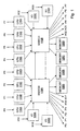
- FIG. 1 Computer System Including Two Switches
- Fig. 1 is a block diagram of a computer system including two switches, switch 110A and switch 110B.
- the computer system includes CPUs 115A-115H, input and output devices (I/O) 120A-120D, and memories 125A-125D.
- Data signals beginning with a P have a processor 115 as a destination, and data signals beginning with an I/O have an I/O device 120 as a destination.
- Switches 110A and 110B are shown receiving input from various groupings of the processors 115 and the I/O devices 120.
- the switches 110A and 110B are also shown outputting signals to various ones of the processors 115, the I/O devices 120, and to the memories 125.
- a plurality of processors (CPUs) 115A-115H each receives an input, preferably addresses, appropriately referenced as P0-P7.
- Each of the processors 115A-115H outputs an output, preferably an address and an address request, such as an address request packet, to one of the two switches 110A and 110B.
- switch 110A also accepts address request packets from I/O device 120A and I/O device 120B.
- switch 110B accepts address request packets from I/O device 120C and I/O device 120D.
- Switch 110A outputs an output signal, preferably address signals, to the CPUs 115A-115D, the I/O devices I/O0-I/O1, and memories 125A-125B.
- Switch 110B outputs an output signal, preferably address signals, to processors 115E-115H, I/O devices I/O2-I/O3, and memories 125C-125D.
- Switch 110A and switch 110B also exchange data. preferably including addresses and address requests.
- processors 115 I/O devices 120, and memories 125 are illustrated. Any number of processors, I/O devices, and/or memories, or other devices are contemplated. It is also noted that while unidirectional data paths are illustrated, bi-directional data paths may also be used as desired.
- Fig. 2 is a block diagram of one embodiment of the switches 110A and 110B.
- each switch 110 includes a plurality of input FIFOs (First-In, First Out buffers) 205, a request arbiter 215, an input multiplexer (MUX) 210, a broadcast FIFO 225, an incoming FIFO 230, a delay circuit 235, a broadcast arbiter 240, and an output MUX 245.
- the switches 110 exchange output requests from their respective request arbiters 215 and output addresses from their respective input MUXes 210.
- switch 110A accepts addresses P0-P3 and I/O0-I/O1, as well as address requests P0_req-P3_req and I/O0_req and I/O1_req.
- Switch 110A outputs address signals P0-P3, I/O0-I/O1, and M0-M1.
- Each incoming address P0-P3 and I/O0-I/O1 is received into an input FIFO 205A-205F.
- the address requests that correspond to the addresses received in the input FIFOs 205A-205F are received at a request arbiter 215A.
- the request arbiter 215A is a round-robin arbiter, although any other means of arbitration may be used as desired for choosing requests received by request arbiter 215A.
- the request arbiter 215A controls the selection at input MUX 210A with regard to the output of the input FIFOs 205A-205F.
- the selected address request is output as SW0_req to delay circuit 235A.
- the output of input MUX 210A, shown as signal 220A is provided to a broadcast FIFO 225A. It is noted that output signal 220A is also provided to switch 110B, and that the address request SW0_req is also provided to switch 110B.
- Switch 110A is also coupled to receive the address request SWI_req from switch 110B, as well as address output signal 220B.
- Signal 220B is received at incoming FIFO 230A.
- broadcast FIFO 225A and incoming FIFO 230A each output data to output MUX 245A, broadcast FIFO 225A as '0' (zero) and incoming FIFO 230A as '1' (one).
- Address request SW0_req is delayed for a period of time in delay circuit 235A before being provided to broadcast arbiter 240A.
- the period of time of the delay may be a predetermined period of time.
- the predetermined period of time is equal to the time required for switch 110A to receive the address request SW1_req and the address output signal 220B.
- Broadcast arbiter 240A chooses (or arbitrates) between request SW0_req and request SW1_req.
- the broadcast arbiter 240A controls the output of output MUX 245A choosing between '0' and '1'.
- the output of output MUX 245A, the selected address for the first transmission, is provided concurrently to various groups of the processors 115, I/O devices 120, and/or memories 125 through signals P0-P3, I/O0-I/O1, and M0-M1.
- switch 110B accepts addresses P4-P7 and I/O2-I/O3, as well as address requests P4_req-P7_req and I/O2_req and I/O3_req.
- Switch 110B outputs address signals P4-P7, I/O2-I/O3, and M2-M3.
- Each incoming address P4-P7 and I/O2-I/O3 is received into an input FIFO 205G-205L.
- the address requests that correspond to the addresses received in the input FIFOs 205G-205L are received at a request arbiter 215B.
- the request arbiter 215B is a round-robin arbiter, although any other means of arbitration may be used as desired for choosing requests received by request arbiter 215B.
- the request arbiter 215B controls the selection at input MUX 210B with regard to the output of the input FIFOs 205G-205L.
- the selected address request is output as SW1_req to delay circuit 235B.
- the output of input MUX 210B. shown as signal 220B, is provided to a broadcast FIFO 225B. It is noted that output signal 220B is also provided to switch 110A, and that the address request SW1_req is also provided to switch 110A.
- Switch 110B is also coupled to receive the address request SW0_req from switch 110A, as well as address output signal 220A.
- Signal 220A is received at incoming FIFO 230B.
- broadcast FIFO 225B and incoming FIFO 230B each output data to output MUX 245B, broadcast FIFO 225B as '1' (one) and incoming FIFO 230B as '0' (zero).
- Address request SW1_req is delayed for a period of time in delay circuit 235B before being provided to broadcast arbiter 240B.
- the period of time of the delay may be a predetermined period of time.
- the predetermined period of time is equal to the time required for switch 110B to receive the address request SW0_req and the address output signal 220A.
- Broadcast arbiter 240B chooses (or arbitrates) between request SW0_req and request SW1_req.
- the broadcast arbiter 240B controls the output of output MUX 245B choosing between '0' and '1'.
- the output of output MUX 245B, the selected address for the first transmission, is provided concurrently to various groups of the processors 115, I/O devices 120, and/or memories 125 through signals P4-P7, I/O2-I/O3, and M2-M3.
- delay circuits 235A and 235B may include any circuit that is configured to delay the output of a received signal.
- a delay circuit 235 delays the received signal longer than the minimum time required to propagate the received signal through delay circuit 235.
- delay circuit 235 includes one or more flip-flops. It is also noted that in various embodiments various incoming and outgoing signals to and from switches 110A and 110B may be buffered at input to the switch 110 and/or on output from the switch 110.
- the first switch 110A is coupled to receive address requests from a first plurality of sources.
- one plurality of sources may be processors 115A-115D and/or I/O devices 120A-120B.
- the first switch 110A is configured to output a received address request from the first plurality of sources.
- the second switch 110B is coupled to receive address requests from a second plurality of sources.
- the second plurality of sources may include processors 115E-115H and/or I/O devices 120C-120D.
- Switch 110B is also configured to receive the address request from the first plurality of sources from the first switch 110A.
- the second switch is further configured to delay internally address requests from the second plurality of sources. It is noted that the length of the delay may be predetermined, and is preferably equal in length of time to the time delay in receiving the address request from the first plurality of sources from the first switch.
- the second switch 110B is further configured to arbitrate between ones of the address requests from the second plurality of sources and ones of the address request from the first plurality of sources output from the first switch.
- the arbitration between the address requests is to determine a selected address request. Once a selected address request has been selected, the first switch and the second switch are further configured to broadcast concurrently the corresponding address to the selected address request. It is noted that the corresponding address will broadcast to any or all devices, including the CPUs 115A-115H, I/O devices 120A-120B, and memories 125A-125D.
- the second switch 110B is further configured to output the address request from the second plurality of sources
- the first switch 110A is further configured to receive this request from the second plurality of sources.
- First switch 110A is further configured to delay internally the address request from the first plurality of sources.
- the time of the delay of the address request from the first plurality of sources may be a predetermined length of time and is preferably a length of time approximately equal to the time required for the second switch 110B to provide the address request in the second plurality of sources to first switch 110A.
- the first switch is further configured to arbitrate between ones of the address request from the first plurality of sources and ones of the address requests from the second plurality of sources from the second switch. The arbitration is to determine the selected address request, as noted above for the second switch 110B. It is noted that the selected address provided by the first switch 110A and the selected address provided by the second switch 110B are the same and are concurrently provided to the devices as described above.
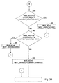
- Figs. 3A and 3B illustrate a flowchart of an embodiment of a method for operating an arbiter, such as broadcast arbiters 240A and 240B.
- the method tracks which switch was most recently selected, and the method also tracks which switch is next to be selected.
- decision block 305 the method checks to see if reset has been asserted. If reset has been asserted in decision box 305, then an output MUX selects output '0' (i.e. switch 110A) and the next granted switch will be the other switch (i.e. switch 110B) (step 310).
- the method determines if only a local request has been made to the first switch 110A or only a remote request has been made to the second switch 110B in decision block 315. If only a local request has been made to the first switch 110A or only a remote request is made to the second switch 110B, then the method selects output MUX output '0' and the next granted switch will be the same switch (step 320).
- the method moves to decision block 325. If only a local request has been made to the second switch 110B or only a remote request has been made to the first switch 110A in decision box 325, then the method selects output MUX output '1' and the next granted switch will be the same switch (step 330).
- decision block 335 if both a local request and a remote request have concurrently been made, and the current granted switch is switch 110A, then the output MUX selects '1' and the next granted switch is switch 110A (step 340). If in decision block 335 both the local request and remote request have been made concurrently but the current granted switch is not switch 0, then the method moves to decision block 345.
- decision block 345 if both the local request and a remote request have been made concurrently and the current granted switch is switch 110B, then the output MUX selects '0' and the next granted switch is switch 110A (step 350). It is noted that in decision blocks 335 and 345, an affirmative decision is made in either case when a local request and a remote request have both been made concurrently. In either case the selected output MUX output is to the switch not most recently selected and the indicated switch as the next granted switch is also the switch not most recently selected.
- the default action when all decision blocks are negative, is for the outgoing MUX to select '0', and the next granted switch is the current granted switch (step 355).
- the switches 110A and 110B may be application specific integrated circuits ASIC0 and ASIC1.
- ASIC0 and ASIC1 are location strapped via jumpers. It is noted that ASIC0 preferably will have a pull-up resistor, while ASIC1 preferably has a pull-down resistor, both of which get latched on reset to identify which is ASIC0 and which is ASIC1. Note that the priority toggles between the broadcast arbiters based on the switch that had the last request granted and the current outstanding request. The method disclosed may advantageously ensure that both arbiters are synchronized to each other without a need for request/grant flow control mechanisms beyond the address and the corresponding address request that was initially received.
- both processors 115A and 115E have an outstanding address packet in the address network.
- the P0 address packet is received in switch 110A's input FIFO 205A from processor 115A
- the P4 address packet is received and stored in switch 110B's input FIFO 205G from processor 115E.
- the request arbiter 215A in switch 110A will receive the P0 request associated with the address stored in input FIFO 205A.
- request arbiter 215B receives the P4_req address request associated with the P4 address stored in input FIFO 205G.
- Request arbiter 215A in switch 110A controls input MUX 210A to output the address associated with input signal P0 as output signal 220A, which is provided to broadcast FIFO 225A and to incoming FIFO 230B.
- request arbiter 215B controls input MUX 210B to output the address from P4 as output signal 220B.
- Output signal 220B is provided to broadcast FIFO 225B and also to incoming FIFO 230A.
- switch 110A Concurrently with the addresses being routed from the input FIFO 205 to the broadcast FIFOs 225 and incoming FIFOs 230, switch 110A has asserted SW0_req line indicating the presence of an address from switch 110A in broadcast FIFO 225A and incoming FIFO 230B.
- signal SW0_req is first provided to a delay circuit 235A, before being provided to broadcast arbiter 240A.
- the delay circuit 235A delays the address request SW0_req by approximately an equal amount of time as required for switch 110A to receive the address and corresponding address request from switch 110B.
- broadcast arbiter 240A receives notice that an address is present in the broadcast FIFO 225A concurrently with an address being available in the incoming FIFO 230A.
- the broadcast arbiter 240A chooses (or arbitrates) for priority between the SW0_req and SW1_req.
- the preferred arbitration method is described above with respect to Figs, 3A and 3B.
- Broadcast arbiter 240A selects either '0' or '1' denoting the address from switch 110A or switch 110B, respectively, in controlling the output of the output multiplexer 245A.
- each switch 110A and 110B delays the address request that it sends, SW0_req and SW1_req, respectively, to the broadcast arbiter 240 of the other switch by an equivalent time period of 2 clock cycles. This delay ensures that the broadcast arbiters 240A and 240B in each switch 110A and 110B receive the address request concurrently.
- Switch 110A has the P0 address placed in its broadcast FIFO 225A and the P4 address placed in incoming FIFO 230A.
- Switch 110B has the P0 address placed in its incoming FIFO 230B and P4 packet placed in broadcast FIFO 225B.
- broadcast arbiter 240A has received address request SW0_req and address request SW1_req, whereas broadcast arbiter 240B has likewise received address request SW0_req and address request SW1_req.
- the arbitration method described above with respect to Figs. 3A and 3B illustrates a preferred embodiment of how the broadcast arbiter 245 works for each address request that it receives.
- the last granted switch defaults to switch 110A, so that switch 110A broadcast arbiter now has the highest priority.
- both broadcast arbiter 240A and broadcast arbiter 240B will select the '0' of the multiplexer 245B. It is noted that both broadcast arbiter 240A and broadcast arbiter 240B are at decision block 345 of Fig. 3B.
- the output MUXes 245 will select '1' and the next granted will be switch 110B (step 330).
- broadcast arbiter 240A and broadcast arbiter 240B following an arbitration method similar to that disclosed in Figs. 3A and 3B, make selections between local and remote requests which are identical in all cases. It is also noted the broadcaster arbiter 240A knows that upon a reset that it will have priority just as broadcast arbiter 240B knows that after a reset it will not have priority.
Landscapes
- Engineering & Computer Science (AREA)
- Physics & Mathematics (AREA)
- Theoretical Computer Science (AREA)
- Computer Hardware Design (AREA)
- General Physics & Mathematics (AREA)
- General Engineering & Computer Science (AREA)
- Software Systems (AREA)
- Mathematical Physics (AREA)
- Multi Processors (AREA)
- Small-Scale Networks (AREA)
- Data Exchanges In Wide-Area Networks (AREA)
- Circuits Of Receivers In General (AREA)
- Two-Way Televisions, Distribution Of Moving Picture Or The Like (AREA)
Claims (19)
- System für das gleichzeitige Bereitstellen von Adressen für eine Mehrzahl von Einrichtungen (115, 120, 125), gekennzeichnet durch:wobei der erste Schalter und der zweite Schalter weiterhin so ausgelegt sind, daß sie gleichzeitig eine Adresse aussenden, welche der ausgewählten Adreßanforderung entspricht.einen ersten Schalter (110A), der dafür ausgelegt ist, daß er eine erste Adreßanforderung von einer ersten Quelle (115A-D, 120A-B, 110B) empfängt, wobei der erste Schalter weiterhin so ausgestattet ist, daß er die erste Adreßanforderung ausgibt, undeinen zweiten Schalter (110B), der dafür ausgelegt ist, daß er eine zweite Adreßanforderung von einer zweiten Quelle (115E-H, 120C-D, 110A) empfängt, und die erste Adreßanforderung empfängt, welche von dem ersten Schalter ausgegeben wurde, wobei der zweite Schalter dafür ausgestaltet ist, daß er die zweite Adreßanforderung verzögert, und weiterhin so ausgestaltet ist, daß er zwischen entweder der ersten Adreßanforderung oder der zweiten Adreßanforderung vermittelt und auswählt,
- System nach Anspruch 1, wobei der zweite Schalter dafür ausgelegt ist, die zweite Adreßanforderung auszugeben und der erste Schalter dafür ausgelegt ist, die zweite Adreßanforderung zu empfangen, die von dem zweiten Schalter ausgegeben wird, und wobei der erste Schalter so ausgestaltet ist, daß er die erste Adreßanforderung verzögert und weiterhin dafür ausgelegt ist, zwischen der ersten Adreßanforderung und der zweiten Adreßanforderung zu vermitteln und die ausgewählte Adreßanforderung auszuwählen.
- System nach Anspruch 1 oder 2, wobei die Verzögerung eine vorbestimmte Zeitdauer hat.
- System nach Anspruch 3, wobei die vorbestimmte Zeitdauer näherungsweise einem Zeitabschnitt entspricht, während dessen die erste Adreßanforderung von dem ersten Schalter zu dem zweiten Schalter transportiert wird.
- System nach einem der vorstehenden Ansprüche, wobei der zweite Schalter aufweist:einen Aussendepuffer (225), der so angeschlossen ist, daß er Adressen emp fängt, welche den Adreßanforderungen, welche von der zweiten Quelle empfangen wur den, entspricht,einen Eingangspuffer (230), der so angeschlossen ist, daß er Adressen empfängt, welche den Adreßanforderungen entsprechen, welche von dem ersten Schalter empfangen wurden,einen Verzögerungsschaltkreis (235), der so ausgestaltet ist, daß er die Verzögerung bereitstellt, wobei der Verzögerungsschaltkreis so angeschlossen ist, daß er die Adreßanforderungen von der zweiten Quelle empfängt, undeinen Aussendevermittler (240), der so ausgestaltet ist, daß er eine Vermittlung zwischen der zweiten Adreßanforderung und der ersten Adreßanforderung ausführt.
- System nach einem der vorstehenden Ansprüche, wobei die zweite Quelle eine Mehrzahl von Einrichtungen (115, 120, 125) aufweist.
- System nach einem der vorstehenden Ansprüche, wobei der zweite Schalter weiterhin aufweist:eine Mehrzahl von Eingangspuffern (205), die so angeschlossen sind, daß sie Adressen empfangen, welche den Adreßanforderungen entsprechen, welche von der zweiten Quelle empfangen wurden,einen Eingangsmultiplexer (210), der so angeschlossen ist, daß er die Adressen von der Mehrzahl von Eingangspuffern empfängt, wobei der Eingangsmultiplexer so ausgestaltet ist, daß er eine ausgewählte Adresse (220) der Adressen in den Aussendepuffer ausgibt, undeinen Anforderungsvermittler (215), der so angeschlossen ist, daß er die Adreßanforderungen von der zweiten Quelle empfängt und zwischen diesen vermittelt, und wobei der Anforderungsvermittler weiterhin so ausgestaltet ist, daß er den Eingangsmultiplexer derart steuert, daß er die ausgewählte Adresse auswählt, wobei der Anforderungsvermittler weiterhin so ausgestaltet ist, daß er die Adreßanforderung von dem Verzögerungsschaltkreis ausgibt, welche der ausgewählten Adresse entspricht.
- System nach einem der vorstehenden Ansprüche, wobei die Mehrzahl von Einrichtungen einen oder mehrere Prozessoren (115) und einen oder mehrere Speicher (125) aufweist.
- System nach Anspruch 8, wobei die Mehrzahl von Einrichtungen weiterhin eine oder mehrere Eingabe-/Ausgabeeinrichtungen (120) umfaßt.
- Verfahren für das gleichzeitige Bereitstellen von Adressen zu einer Mehrzahl von Einrichtungen (115, 120, 125), wobei das Verfahren gekennzeichnet ist durch:Empfangen einer ersten Adresse und einer entsprechenden ersten Anforderung von einer ersten Quelle (115A-D, 120A-B, 110B) an einem ersten Schalter (110A),Empfangen einer zweiten Adresse und einer entsprechenden zweiten Anforderung von einer zweiten Quelle (115E-H, 120C-D, 110A) an einem zweiten Schalter (110B),Transportieren der zweiten Adresse und der entsprechenden zweiten Adreßanforderung an den ersten Schalter,Verzögern der ersten Anforderung in dem ersten Schalter,Vermitteln in dem ersten Schalter zwischen der ersten Anforderung und der zweiten Anforderung bezüglich einer ersten Übermittlung entweder der ersten Adresse oder der zweiten Adresse, undgleichzeitiges Aussenden der ersten Übermittlung von dem ersten Schalter und der ersten Übermittlung von dem zweiten Schalter an eine Mehrzahl von Einrichtungen, wobei die erste Übermittlung von dem ersten Schalter und die erste Übermittlung von dem zweiten Schalter identisch sind.
- Verfahren nach Anspruch 10, welches weiterhin aufweist:Transportieren der ersten Adresse und der entsprechenden ersten Anforderung an den zweiten Schalter,Verzögern der entsprechenden zweiten Anforderung in dem zweiten Schalter, undVermitteln in dem zweiten Schalter zwischen der entsprechenden ersten Anforderung und der entsprechenden zweiten Anforderung bezüglich der Frage, ob die erste Adresse oder die zweite Adresse die erste Übermittlung aufweist.
- Verfahren nach Anspruch 11, welches weiterhin aufweist:Puffern der ersten Adresse an dem ersten Schalter, bevor die erste Adresse übermittelt wird, undPuffern der zweiten Adresse an dem zweiten Schalter, bevor die zweite Adresse übermittelt wird.
- Verfahren nach Anspruch 11 oder 12, welches weiterhin aufweist:Puffern der ersten Adresse an dem ersten Schalter vor dem Vermitteln in dem ersten Schalter, undPuffern der zweiten Adresse an dem zweiten Schalter vor der Vermittlung in dem zweiten Schalter.
- Verfahren nach einem der Ansprüche 11 bis 13, welches weiterhin aufweist:Puffern der ersten Adresse in dem zweiten Schalter, bevor in dem zweiten Schalter vermittelt wird, undPuffern der zweiten Adresse an dem ersten Schalter vor dem Vermitteln in dem ersten Schalter.
- Verfahren nach einem der Ansprüche 11 bis 14, welches weiterhin aufweist:Empfangen einer anderen Adresse an dem ersten Schalter und einer entsprechenden anderen Anforderung von einer anderen Quelle,Puffern der anderen Adresse an dem ersten Schalter vor dem Übertragen der ersten Adresse, undVermitteln zwischen der entsprechenden ersten Anforderung und der entsprechenden weiteren Anforderung bezüglich der Frage, ob die erste Adresse oder die weitere Adresse von dem zweiten Schalter aus zuerst übertragen wird.
- Verfahren nach irgendeinem der Ansprüche 11 bis 15, welches weiterhin aufweist:Empfangen einer zusätzlichen Adresse und einer entsprechenden zusätzlichen Anforderung von einer zusätzlichen Quelle an dem zweiten Schalter,Puffern der zusätzlichen Adresse an dem zweiten Schalter vor dem Übermitteln der zweiten Adresse, undVermitteln zwischen der entsprechenden zweiten Anforderung und der entsprechenden zusätzlichen Anforderung der Frage, ob die zweite Adresse oder die zusätzliche Adresse zuerst an den ersten Schalter übertragen wird.
- Verfahren nach einem der Ansprüche 11 bis 16, wobei das Verzögern der entsprechenden ersten Anforderung in dem ersten Schalter das Verzögern der Anforderungen von dem zweiten Schalter um näherungsweise einen Zeitabschnitt bis zum Erreichen des ersten Schalters aufweist, und wobei das Verzögern einer entsprechenden zweiten Anforderung in dem zweiten Schritt das Verzögern um näherungsweise einen Zeitabschnitt aufweist, der benötigt wird, damit die Anforderung von dem ersten Schalter an dem zweiten Schalter ankommt.
- Verfahren nach einem der Ansprüche 11 bis 17, wobei die Vermittlung aufweist:Verfolgen, welcher Schalter zuletzt ausgewählt worden war,Verfolgen, welcher Schalter als nächstes ausgewählt werden soll,in Reaktion auf eine Zurückstellung (reset), Auswählen des ersten Schalters und Anzeigen des zweiten Schalters als als nächstes auszuwählender,in Reaktion auf nur eine lokale Anforderung an den ersten Schalter oder nur eine aus der Ferne kommende Anforderung an den zweiten Schalter, Auswählen des ersten Schalters undKennzeichnen des ersten Schalters als als nächstes auszuwählender,in Reaktion auf nur eine lokale Anforderung an den zweiten Schalter oder nur eine Fernanforderung an den ersten Schalter, Auswählen des zweiten Schalters und Kennzeichnen des zweiten Schalters als als nächstes auszuwählender,in Reaktion auf sowohl eine lokale Anforderung als auch eine gleichzeitige Fernanforderung,Auswählen eines Schalters, der nicht als letzter ausgewählt worden war und Kennzeichen des Schalters, der nicht als letzter ausgewählt worden war, als als nächstes auszuwählender,ansonsten Auswählen des ersten Schalters undKennzeichnen des zuletzt ausgewählten Schalters als als nächstes auszuwählender.
- Verfahren nach Anspruch 18, welches weiterhin aufweist:Kennzeichnen des Schalters, der als nächster auszuwählen ist, und zwar bei einer ansteigenden Flanke eines Taktes.
Applications Claiming Priority (3)
| Application Number | Priority Date | Filing Date | Title |
|---|---|---|---|
| US09/374,639 US6567885B1 (en) | 1999-08-16 | 1999-08-16 | System and method for address broadcast synchronization using a plurality of switches |
| US374639 | 1999-08-16 | ||
| PCT/US2000/022563 WO2001013247A2 (en) | 1999-08-16 | 2000-08-16 | System and method for address broadcast synchronization using a plurality of switches |
Publications (2)
| Publication Number | Publication Date |
|---|---|
| EP1208440A2 EP1208440A2 (de) | 2002-05-29 |
| EP1208440B1 true EP1208440B1 (de) | 2003-04-09 |
Family
ID=23477631
Family Applications (1)
| Application Number | Title | Priority Date | Filing Date |
|---|---|---|---|
| EP00957512A Expired - Lifetime EP1208440B1 (de) | 1999-08-16 | 2000-08-16 | System und verfahren für adressrundfunksynchronisation mit einer mehrzahl von schaltern |
Country Status (6)
| Country | Link |
|---|---|
| US (2) | US6567885B1 (de) |
| EP (1) | EP1208440B1 (de) |
| AT (1) | ATE237156T1 (de) |
| AU (1) | AU6911800A (de) |
| DE (1) | DE60002094D1 (de) |
| WO (1) | WO2001013247A2 (de) |
Families Citing this family (25)
| Publication number | Priority date | Publication date | Assignee | Title |
|---|---|---|---|---|
| US6567885B1 (en) * | 1999-08-16 | 2003-05-20 | Sun Microsystems, Inc. | System and method for address broadcast synchronization using a plurality of switches |
| US6813267B1 (en) * | 2000-09-11 | 2004-11-02 | Sun Microsystems, Inc. | Tunable broadcast/point-to-point packet arbitration |
| US20020133652A1 (en) * | 2001-03-19 | 2002-09-19 | Tai Quan | Apparatus for avoiding starvation in hierarchical computer systems that prioritize transactions |
| US6826643B2 (en) * | 2001-03-19 | 2004-11-30 | Sun Microsystems, Inc. | Method of synchronizing arbiters within a hierarchical computer system |
| US6889343B2 (en) * | 2001-03-19 | 2005-05-03 | Sun Microsystems, Inc. | Method and apparatus for verifying consistency between a first address repeater and a second address repeater |
| US6877055B2 (en) | 2001-03-19 | 2005-04-05 | Sun Microsystems, Inc. | Method and apparatus for efficiently broadcasting transactions between a first address repeater and a second address repeater |
| US6950893B2 (en) * | 2001-03-22 | 2005-09-27 | I-Bus Corporation | Hybrid switching architecture |
| US7376811B2 (en) * | 2001-11-06 | 2008-05-20 | Netxen, Inc. | Method and apparatus for performing computations and operations on data using data steering |
| US7548957B1 (en) | 2002-05-07 | 2009-06-16 | Oracle International Corporation | Method and mechanism for a portal website architecture |
| US7277924B1 (en) * | 2002-05-07 | 2007-10-02 | Oracle International Corporation | Method and mechanism for a portal website architecture |
| JP3770203B2 (ja) * | 2002-05-21 | 2006-04-26 | 日本電気株式会社 | クロスバの高速化方法及びクロスバの高速化方式 |
| US6877056B2 (en) * | 2002-06-28 | 2005-04-05 | Sun Microsystems, Inc. | System with arbitration scheme supporting virtual address networks and having split ownership and access right coherence mechanism |
| GB2409306A (en) * | 2003-12-20 | 2005-06-22 | Autodesk Canada Inc | Data processing network with switchable storage |
| US7451231B2 (en) * | 2005-02-10 | 2008-11-11 | International Business Machines Corporation | Data processing system, method and interconnect fabric for synchronized communication in a data processing system |
| US20060176890A1 (en) * | 2005-02-10 | 2006-08-10 | International Business Machines Corporation | Data processing system, method and interconnect fabric for improved communication in a data processing system |
| US8307147B2 (en) * | 2005-09-09 | 2012-11-06 | Freescale Semiconductor, Inc. | Interconnect and a method for designing an interconnect |
| JP5270077B2 (ja) * | 2006-08-18 | 2013-08-21 | 富士通株式会社 | 調停回路、クロスバ、リクエスト選択方法、及び情報処理装置 |
| US8082381B2 (en) * | 2008-09-02 | 2011-12-20 | Nvidia Corporation | Connecting a plurality of peripherals |
| US8103803B2 (en) * | 2008-11-21 | 2012-01-24 | Nvidia Corporation | Communication between a processor and a controller |
| US8610732B2 (en) * | 2008-12-11 | 2013-12-17 | Nvidia Corporation | System and method for video memory usage for general system application |
| US8677074B2 (en) * | 2008-12-15 | 2014-03-18 | Nvidia Corporation | Shared memory access techniques |
| US8984206B2 (en) * | 2012-10-31 | 2015-03-17 | International Business Machines Corporation | Weightage-based scheduling for hierarchical switching fabrics |
| US8902899B2 (en) | 2013-02-08 | 2014-12-02 | International Business Machines Corporation | Input buffered switching device including bypass logic |
| US9311207B1 (en) * | 2013-09-12 | 2016-04-12 | Emc Corporation | Data storage system optimizations in a multi-tiered environment |
| US9467396B2 (en) | 2014-04-11 | 2016-10-11 | International Business Machines Corporation | Simultaneous transfers from a single input link to multiple output links with a timesliced crossbar |
Family Cites Families (9)
| Publication number | Priority date | Publication date | Assignee | Title |
|---|---|---|---|---|
| US4398176A (en) | 1980-08-15 | 1983-08-09 | Environmental Research Institute Of Michigan | Image analyzer with common data/instruction bus |
| US5179552A (en) * | 1990-11-26 | 1993-01-12 | Bell Communications Research, Inc. | Crosspoint matrix switching element for a packet switch |
| US5166926A (en) | 1990-12-18 | 1992-11-24 | Bell Communications Research, Inc. | Packet address look-ahead technique for use in implementing a high speed packet switch |
| US5513369A (en) | 1991-08-05 | 1996-04-30 | Ncr Corporation | Star coupler device including means for connecting multiple star couplers together in a cascaded relationship |
| US5613071A (en) | 1995-07-14 | 1997-03-18 | Intel Corporation | Method and apparatus for providing remote memory access in a distributed memory multiprocessor system |
| US5862357A (en) | 1996-07-02 | 1999-01-19 | Sun Microsystems, Inc. | Hierarchical SMP computer system |
| US6483844B1 (en) * | 1999-05-13 | 2002-11-19 | Advanced Micro Devices, Inc. | Apparatus and method for sharing an external memory between multiple network switches |
| US6567885B1 (en) * | 1999-08-16 | 2003-05-20 | Sun Microsystems, Inc. | System and method for address broadcast synchronization using a plurality of switches |
| US7020146B2 (en) * | 2001-08-30 | 2006-03-28 | Sun Microsystems, Inc. | Broadcast arbitration in a multi-domain device |
-
1999
- 1999-08-16 US US09/374,639 patent/US6567885B1/en not_active Expired - Lifetime
-
2000
- 2000-08-16 DE DE60002094T patent/DE60002094D1/de not_active Expired - Lifetime
- 2000-08-16 WO PCT/US2000/022563 patent/WO2001013247A2/en not_active Ceased
- 2000-08-16 AT AT00957512T patent/ATE237156T1/de not_active IP Right Cessation
- 2000-08-16 AU AU69118/00A patent/AU6911800A/en not_active Abandoned
- 2000-08-16 EP EP00957512A patent/EP1208440B1/de not_active Expired - Lifetime
-
2003
- 2003-04-02 US US10/405,876 patent/US6678784B2/en not_active Expired - Lifetime
Also Published As
| Publication number | Publication date |
|---|---|
| US6678784B2 (en) | 2004-01-13 |
| WO2001013247A3 (en) | 2001-08-30 |
| US20030191879A1 (en) | 2003-10-09 |
| US6567885B1 (en) | 2003-05-20 |
| AU6911800A (en) | 2001-03-13 |
| WO2001013247A9 (en) | 2001-09-20 |
| EP1208440A2 (de) | 2002-05-29 |
| WO2001013247A2 (en) | 2001-02-22 |
| DE60002094D1 (de) | 2003-05-15 |
| ATE237156T1 (de) | 2003-04-15 |
Similar Documents
| Publication | Publication Date | Title |
|---|---|---|
| EP1208440B1 (de) | System und verfahren für adressrundfunksynchronisation mit einer mehrzahl von schaltern | |
| US5805589A (en) | Central shared queue based time multiplexed packet switch with deadlock avoidance | |
| US5623644A (en) | Point-to-point phase-tolerant communication | |
| US6715023B1 (en) | PCI bus switch architecture | |
| US7584320B2 (en) | Sliced crossbar architecture with no inter-slice communication | |
| JPH02234543A (ja) | デイジタル交換装置、メツセージ・コンバイニング・スイツチ及びその動作方法 | |
| US7353310B2 (en) | Hierarchical memory access via pipelining with deferred arbitration | |
| EP0866404A2 (de) | Unsymmetrische Multiplexer- und Arbiter-Kombination | |
| US7054969B1 (en) | Apparatus for use in a computer system | |
| US6970454B1 (en) | Sliced crossbar architecture with inter-slice communication | |
| GB2484483A (en) | Communication on integrated circuit using interconnect circuitry | |
| US6826643B2 (en) | Method of synchronizing arbiters within a hierarchical computer system | |
| US20070299993A1 (en) | Method and Device for Treating and Processing Data | |
| US5420853A (en) | Self controlling crossbar switch and method | |
| EP1187422B1 (de) | Verfahren und Vorrichtung zur einstellbaren Paketarbitrierung | |
| JP2882304B2 (ja) | マルチプロセッサシステム | |
| Wang et al. | System-on-chip communication architecture: dynamic parallel fraction control bus design and test methodologies | |
| JP2009032281A (ja) | データ伝送方法 | |
| GB2341765A (en) | Bus idle usage | |
| GB2341769A (en) | Data packet reordering | |
| GB2341770A (en) | Modular bus topology | |
| GB2341768A (en) | Bus arbitration | |
| GB2341699A (en) | Inter-module data transfer |
Legal Events
| Date | Code | Title | Description |
|---|---|---|---|
| PUAI | Public reference made under article 153(3) epc to a published international application that has entered the european phase |
Free format text: ORIGINAL CODE: 0009012 |
|
| 17P | Request for examination filed |
Effective date: 20020301 |
|
| AK | Designated contracting states |
Kind code of ref document: A2 Designated state(s): AT BE CH CY DE DK ES FI FR GB GR IE IT LI LU MC NL PT |
|
| AX | Request for extension of the european patent |
Free format text: AL;LT;LV;MK;RO;SI |
|
| GRAG | Despatch of communication of intention to grant |
Free format text: ORIGINAL CODE: EPIDOS AGRA |
|
| 17Q | First examination report despatched |
Effective date: 20020621 |
|
| GRAG | Despatch of communication of intention to grant |
Free format text: ORIGINAL CODE: EPIDOS AGRA |
|
| GRAH | Despatch of communication of intention to grant a patent |
Free format text: ORIGINAL CODE: EPIDOS IGRA |
|
| GRAH | Despatch of communication of intention to grant a patent |
Free format text: ORIGINAL CODE: EPIDOS IGRA |
|
| GRAA | (expected) grant |
Free format text: ORIGINAL CODE: 0009210 |
|
| AK | Designated contracting states |
Designated state(s): AT BE CH CY DE DK ES FI FR GB GR IE IT LI LU MC NL PT |
|
| PG25 | Lapsed in a contracting state [announced via postgrant information from national office to epo] |
Ref country code: IT Free format text: LAPSE BECAUSE OF FAILURE TO SUBMIT A TRANSLATION OF THE DESCRIPTION OR TO PAY THE FEE WITHIN THE PRESCRIBED TIME-LIMIT;WARNING: LAPSES OF ITALIAN PATENTS WITH EFFECTIVE DATE BEFORE 2007 MAY HAVE OCCURRED AT ANY TIME BEFORE 2007. THE CORRECT EFFECTIVE DATE MAY BE DIFFERENT FROM THE ONE RECORDED. Effective date: 20030409 Ref country code: NL Free format text: LAPSE BECAUSE OF FAILURE TO SUBMIT A TRANSLATION OF THE DESCRIPTION OR TO PAY THE FEE WITHIN THE PRESCRIBED TIME-LIMIT Effective date: 20030409 Ref country code: LI Free format text: LAPSE BECAUSE OF FAILURE TO SUBMIT A TRANSLATION OF THE DESCRIPTION OR TO PAY THE FEE WITHIN THE PRESCRIBED TIME-LIMIT Effective date: 20030409 Ref country code: FI Free format text: LAPSE BECAUSE OF FAILURE TO SUBMIT A TRANSLATION OF THE DESCRIPTION OR TO PAY THE FEE WITHIN THE PRESCRIBED TIME-LIMIT Effective date: 20030409 Ref country code: FR Free format text: LAPSE BECAUSE OF FAILURE TO SUBMIT A TRANSLATION OF THE DESCRIPTION OR TO PAY THE FEE WITHIN THE PRESCRIBED TIME-LIMIT Effective date: 20030409 Ref country code: CH Free format text: LAPSE BECAUSE OF FAILURE TO SUBMIT A TRANSLATION OF THE DESCRIPTION OR TO PAY THE FEE WITHIN THE PRESCRIBED TIME-LIMIT Effective date: 20030409 Ref country code: BE Free format text: LAPSE BECAUSE OF FAILURE TO SUBMIT A TRANSLATION OF THE DESCRIPTION OR TO PAY THE FEE WITHIN THE PRESCRIBED TIME-LIMIT Effective date: 20030409 |
|
| REG | Reference to a national code |
Ref country code: GB Ref legal event code: FG4D |
|
| REG | Reference to a national code |
Ref country code: CH Ref legal event code: EP |
|
| PG25 | Lapsed in a contracting state [announced via postgrant information from national office to epo] |
Ref country code: AT Free format text: LAPSE BECAUSE OF FAILURE TO SUBMIT A TRANSLATION OF THE DESCRIPTION OR TO PAY THE FEE WITHIN THE PRESCRIBED TIME-LIMIT Effective date: 20030423 |
|
| RAP2 | Party data changed (patent owner data changed or rights of a patent transferred) |
Owner name: SUN MICROSYSTEMS, INC. |
|
| REG | Reference to a national code |
Ref country code: IE Ref legal event code: FG4D |
|
| NLT2 | Nl: modifications (of names), taken from the european patent patent bulletin |
Owner name: SUN MICROSYSTEMS, INC. |
|
| PG25 | Lapsed in a contracting state [announced via postgrant information from national office to epo] |
Ref country code: PT Free format text: LAPSE BECAUSE OF FAILURE TO SUBMIT A TRANSLATION OF THE DESCRIPTION OR TO PAY THE FEE WITHIN THE PRESCRIBED TIME-LIMIT Effective date: 20030709 Ref country code: DK Free format text: LAPSE BECAUSE OF FAILURE TO SUBMIT A TRANSLATION OF THE DESCRIPTION OR TO PAY THE FEE WITHIN THE PRESCRIBED TIME-LIMIT Effective date: 20030709 Ref country code: GR Free format text: LAPSE BECAUSE OF FAILURE TO SUBMIT A TRANSLATION OF THE DESCRIPTION OR TO PAY THE FEE WITHIN THE PRESCRIBED TIME-LIMIT Effective date: 20030709 |
|
| PG25 | Lapsed in a contracting state [announced via postgrant information from national office to epo] |
Ref country code: DE Free format text: LAPSE BECAUSE OF FAILURE TO SUBMIT A TRANSLATION OF THE DESCRIPTION OR TO PAY THE FEE WITHIN THE PRESCRIBED TIME-LIMIT Effective date: 20030710 |
|
| PG25 | Lapsed in a contracting state [announced via postgrant information from national office to epo] |
Ref country code: LU Free format text: LAPSE BECAUSE OF NON-PAYMENT OF DUE FEES Effective date: 20030816 Ref country code: CY Free format text: LAPSE BECAUSE OF FAILURE TO SUBMIT A TRANSLATION OF THE DESCRIPTION OR TO PAY THE FEE WITHIN THE PRESCRIBED TIME-LIMIT Effective date: 20030816 |
|
| PG25 | Lapsed in a contracting state [announced via postgrant information from national office to epo] |
Ref country code: IE Free format text: LAPSE BECAUSE OF NON-PAYMENT OF DUE FEES Effective date: 20030818 |
|
| PG25 | Lapsed in a contracting state [announced via postgrant information from national office to epo] |
Ref country code: MC Free format text: LAPSE BECAUSE OF NON-PAYMENT OF DUE FEES Effective date: 20030831 |
|
| NLV1 | Nl: lapsed or annulled due to failure to fulfill the requirements of art. 29p and 29m of the patents act | ||
| LTIE | Lt: invalidation of european patent or patent extension |
Effective date: 20030409 |
|
| REG | Reference to a national code |
Ref country code: CH Ref legal event code: PL |
|
| PG25 | Lapsed in a contracting state [announced via postgrant information from national office to epo] |
Ref country code: ES Free format text: LAPSE BECAUSE OF FAILURE TO SUBMIT A TRANSLATION OF THE DESCRIPTION OR TO PAY THE FEE WITHIN THE PRESCRIBED TIME-LIMIT Effective date: 20031030 |
|
| PLBE | No opposition filed within time limit |
Free format text: ORIGINAL CODE: 0009261 |
|
| STAA | Information on the status of an ep patent application or granted ep patent |
Free format text: STATUS: NO OPPOSITION FILED WITHIN TIME LIMIT |
|
| EN | Fr: translation not filed | ||
| 26N | No opposition filed |
Effective date: 20040112 |
|
| REG | Reference to a national code |
Ref country code: IE Ref legal event code: MM4A |
|
| PGFP | Annual fee paid to national office [announced via postgrant information from national office to epo] |
Ref country code: GB Payment date: 20190815 Year of fee payment: 20 |
|
| REG | Reference to a national code |
Ref country code: GB Ref legal event code: PE20 Expiry date: 20200815 |
|
| PG25 | Lapsed in a contracting state [announced via postgrant information from national office to epo] |
Ref country code: GB Free format text: LAPSE BECAUSE OF EXPIRATION OF PROTECTION Effective date: 20200815 |