EP1207566A2 - Anode thin film for lithium secondary battery - Google Patents
Anode thin film for lithium secondary battery Download PDFInfo
- Publication number
- EP1207566A2 EP1207566A2 EP01126821A EP01126821A EP1207566A2 EP 1207566 A2 EP1207566 A2 EP 1207566A2 EP 01126821 A EP01126821 A EP 01126821A EP 01126821 A EP01126821 A EP 01126821A EP 1207566 A2 EP1207566 A2 EP 1207566A2
- Authority
- EP
- European Patent Office
- Prior art keywords
- thin film
- layer
- anode
- active material
- thickness
- Prior art date
- Legal status (The legal status is an assumption and is not a legal conclusion. Google has not performed a legal analysis and makes no representation as to the accuracy of the status listed.)
- Granted
Links
- 239000010409 thin film Substances 0.000 title claims abstract description 110
- 229910052744 lithium Inorganic materials 0.000 title claims abstract description 44
- WHXSMMKQMYFTQS-UHFFFAOYSA-N Lithium Chemical compound [Li] WHXSMMKQMYFTQS-UHFFFAOYSA-N 0.000 title claims abstract description 38
- 239000010410 layer Substances 0.000 claims abstract description 116
- 239000006183 anode active material Substances 0.000 claims abstract description 43
- 229910052710 silicon Inorganic materials 0.000 claims abstract description 37
- 229910052709 silver Inorganic materials 0.000 claims abstract description 30
- XUIMIQQOPSSXEZ-UHFFFAOYSA-N Silicon Chemical compound [Si] XUIMIQQOPSSXEZ-UHFFFAOYSA-N 0.000 claims abstract description 26
- 239000002365 multiple layer Substances 0.000 claims abstract description 25
- 239000010703 silicon Substances 0.000 claims abstract description 25
- BQCADISMDOOEFD-UHFFFAOYSA-N Silver Chemical compound [Ag] BQCADISMDOOEFD-UHFFFAOYSA-N 0.000 claims abstract description 16
- 239000004332 silver Substances 0.000 claims abstract description 16
- 239000002356 single layer Substances 0.000 claims abstract description 15
- 239000010949 copper Substances 0.000 claims description 17
- PXHVJJICTQNCMI-UHFFFAOYSA-N Nickel Chemical compound [Ni] PXHVJJICTQNCMI-UHFFFAOYSA-N 0.000 claims description 10
- RYGMFSIKBFXOCR-UHFFFAOYSA-N Copper Chemical compound [Cu] RYGMFSIKBFXOCR-UHFFFAOYSA-N 0.000 claims description 5
- 229910052802 copper Inorganic materials 0.000 claims description 5
- ZOKXTWBITQBERF-UHFFFAOYSA-N Molybdenum Chemical compound [Mo] ZOKXTWBITQBERF-UHFFFAOYSA-N 0.000 claims description 3
- 229910052750 molybdenum Inorganic materials 0.000 claims description 3
- 239000011733 molybdenum Substances 0.000 claims description 3
- 229910052759 nickel Inorganic materials 0.000 claims description 3
- LEONUFNNVUYDNQ-UHFFFAOYSA-N vanadium atom Chemical compound [V] LEONUFNNVUYDNQ-UHFFFAOYSA-N 0.000 claims description 3
- 238000007599 discharging Methods 0.000 description 13
- 230000002427 irreversible effect Effects 0.000 description 10
- 238000000151 deposition Methods 0.000 description 9
- 238000010586 diagram Methods 0.000 description 9
- 238000004544 sputter deposition Methods 0.000 description 9
- 108010057081 Merozoite Surface Protein 1 Proteins 0.000 description 8
- 239000011149 active material Substances 0.000 description 7
- 230000008021 deposition Effects 0.000 description 7
- 230000008859 change Effects 0.000 description 6
- 239000003792 electrolyte Substances 0.000 description 6
- 239000000463 material Substances 0.000 description 6
- 238000000034 method Methods 0.000 description 6
- 239000000203 mixture Substances 0.000 description 6
- APCLRHPWFCQIMG-UHFFFAOYSA-N 4-(5,6-dimethoxy-1-benzothiophen-2-yl)-4-oxobutanoic acid Chemical compound C1=C(OC)C(OC)=CC2=C1SC(C(=O)CCC(O)=O)=C2 APCLRHPWFCQIMG-UHFFFAOYSA-N 0.000 description 5
- 229940125791 MSA-2 Drugs 0.000 description 5
- 101710162106 Merozoite surface antigen 2 Proteins 0.000 description 5
- 229910045601 alloy Inorganic materials 0.000 description 5
- 239000000956 alloy Substances 0.000 description 5
- 230000000052 comparative effect Effects 0.000 description 5
- 238000001704 evaporation Methods 0.000 description 5
- VYPSYNLAJGMNEJ-UHFFFAOYSA-N Silicium dioxide Chemical compound O=[Si]=O VYPSYNLAJGMNEJ-UHFFFAOYSA-N 0.000 description 4
- 230000008020 evaporation Effects 0.000 description 4
- 238000007735 ion beam assisted deposition Methods 0.000 description 4
- 239000000758 substrate Substances 0.000 description 4
- 238000006243 chemical reaction Methods 0.000 description 3
- 230000000694 effects Effects 0.000 description 3
- 230000004907 flux Effects 0.000 description 3
- 239000007789 gas Substances 0.000 description 3
- 150000002500 ions Chemical class 0.000 description 3
- 230000009467 reduction Effects 0.000 description 3
- 238000011160 research Methods 0.000 description 3
- 239000004065 semiconductor Substances 0.000 description 3
- XKRFYHLGVUSROY-UHFFFAOYSA-N Argon Chemical compound [Ar] XKRFYHLGVUSROY-UHFFFAOYSA-N 0.000 description 2
- OIFBSDVPJOWBCH-UHFFFAOYSA-N Diethyl carbonate Chemical compound CCOC(=O)OCC OIFBSDVPJOWBCH-UHFFFAOYSA-N 0.000 description 2
- KMTRUDSVKNLOMY-UHFFFAOYSA-N Ethylene carbonate Chemical compound O=C1OCCO1 KMTRUDSVKNLOMY-UHFFFAOYSA-N 0.000 description 2
- 229910000733 Li alloy Inorganic materials 0.000 description 2
- 229910008266 Li-Ag Inorganic materials 0.000 description 2
- 229910008445 Li—Ag Inorganic materials 0.000 description 2
- 238000005336 cracking Methods 0.000 description 2
- 238000009831 deintercalation Methods 0.000 description 2
- 238000013461 design Methods 0.000 description 2
- 230000006866 deterioration Effects 0.000 description 2
- 230000002542 deteriorative effect Effects 0.000 description 2
- 238000009826 distribution Methods 0.000 description 2
- GNTDGMZSJNCJKK-UHFFFAOYSA-N divanadium pentaoxide Chemical compound O=[V](=O)O[V](=O)=O GNTDGMZSJNCJKK-UHFFFAOYSA-N 0.000 description 2
- 239000008151 electrolyte solution Substances 0.000 description 2
- 238000011156 evaluation Methods 0.000 description 2
- 239000010408 film Substances 0.000 description 2
- 238000009830 intercalation Methods 0.000 description 2
- 230000002687 intercalation Effects 0.000 description 2
- 238000010884 ion-beam technique Methods 0.000 description 2
- 239000001989 lithium alloy Substances 0.000 description 2
- WUALQPNAHOKFBR-UHFFFAOYSA-N lithium silver Chemical compound [Li].[Ag] WUALQPNAHOKFBR-UHFFFAOYSA-N 0.000 description 2
- 238000004519 manufacturing process Methods 0.000 description 2
- 229910052751 metal Inorganic materials 0.000 description 2
- 239000002184 metal Substances 0.000 description 2
- 238000012858 packaging process Methods 0.000 description 2
- 238000012545 processing Methods 0.000 description 2
- 239000000377 silicon dioxide Substances 0.000 description 2
- 239000002409 silicon-based active material Substances 0.000 description 2
- 239000011856 silicon-based particle Substances 0.000 description 2
- 239000007784 solid electrolyte Substances 0.000 description 2
- 239000000126 substance Substances 0.000 description 2
- 229910052720 vanadium Inorganic materials 0.000 description 2
- 229910017941 Ag—Li Inorganic materials 0.000 description 1
- 229910032387 LiCoO2 Inorganic materials 0.000 description 1
- 229910001290 LiPF6 Inorganic materials 0.000 description 1
- HBBGRARXTFLTSG-UHFFFAOYSA-N Lithium ion Chemical compound [Li+] HBBGRARXTFLTSG-UHFFFAOYSA-N 0.000 description 1
- 229910002097 Lithium manganese(III,IV) oxide Inorganic materials 0.000 description 1
- 229910018530 Si-Ag Inorganic materials 0.000 description 1
- 229910006950 Si0.6Ag0.4 Inorganic materials 0.000 description 1
- 229910000681 Silicon-tin Inorganic materials 0.000 description 1
- 229910008383 Si—Ag Inorganic materials 0.000 description 1
- ATJFFYVFTNAWJD-UHFFFAOYSA-N Tin Chemical compound [Sn] ATJFFYVFTNAWJD-UHFFFAOYSA-N 0.000 description 1
- ZVLDJSZFKQJMKD-UHFFFAOYSA-N [Li].[Si] Chemical compound [Li].[Si] ZVLDJSZFKQJMKD-UHFFFAOYSA-N 0.000 description 1
- XNRNVYYTHRPBDD-UHFFFAOYSA-N [Si][Ag] Chemical compound [Si][Ag] XNRNVYYTHRPBDD-UHFFFAOYSA-N 0.000 description 1
- 229910052782 aluminium Inorganic materials 0.000 description 1
- XAGFODPZIPBFFR-UHFFFAOYSA-N aluminium Chemical compound [Al] XAGFODPZIPBFFR-UHFFFAOYSA-N 0.000 description 1
- 229910052786 argon Inorganic materials 0.000 description 1
- QVGXLLKOCUKJST-UHFFFAOYSA-N atomic oxygen Chemical compound [O] QVGXLLKOCUKJST-UHFFFAOYSA-N 0.000 description 1
- 230000003139 buffering effect Effects 0.000 description 1
- 230000000295 complement effect Effects 0.000 description 1
- 238000000354 decomposition reaction Methods 0.000 description 1
- 230000003247 decreasing effect Effects 0.000 description 1
- 238000011161 development Methods 0.000 description 1
- 239000007772 electrode material Substances 0.000 description 1
- 238000010894 electron beam technology Methods 0.000 description 1
- 238000005530 etching Methods 0.000 description 1
- 238000010438 heat treatment Methods 0.000 description 1
- 230000006872 improvement Effects 0.000 description 1
- LQJIDIOGYJAQMF-UHFFFAOYSA-N lambda2-silanylidenetin Chemical compound [Si].[Sn] LQJIDIOGYJAQMF-UHFFFAOYSA-N 0.000 description 1
- 239000011244 liquid electrolyte Substances 0.000 description 1
- 229910001416 lithium ion Inorganic materials 0.000 description 1
- 238000002844 melting Methods 0.000 description 1
- 230000008018 melting Effects 0.000 description 1
- 229910044991 metal oxide Inorganic materials 0.000 description 1
- 150000004706 metal oxides Chemical class 0.000 description 1
- 238000004377 microelectronic Methods 0.000 description 1
- 239000011859 microparticle Substances 0.000 description 1
- 239000012046 mixed solvent Substances 0.000 description 1
- 238000002156 mixing Methods 0.000 description 1
- 238000012986 modification Methods 0.000 description 1
- 230000004048 modification Effects 0.000 description 1
- 239000002105 nanoparticle Substances 0.000 description 1
- 150000004767 nitrides Chemical class 0.000 description 1
- 239000001301 oxygen Substances 0.000 description 1
- 229910052760 oxygen Inorganic materials 0.000 description 1
- 239000002245 particle Substances 0.000 description 1
- 230000008569 process Effects 0.000 description 1
- 239000000376 reactant Substances 0.000 description 1
- 230000009257 reactivity Effects 0.000 description 1
- 238000007086 side reaction Methods 0.000 description 1
- 235000012239 silicon dioxide Nutrition 0.000 description 1
- 238000005476 soldering Methods 0.000 description 1
- -1 that is Substances 0.000 description 1
- 238000007669 thermal treatment Methods 0.000 description 1
Images


Classifications
-
- H—ELECTRICITY
- H01—ELECTRIC ELEMENTS
- H01M—PROCESSES OR MEANS, e.g. BATTERIES, FOR THE DIRECT CONVERSION OF CHEMICAL ENERGY INTO ELECTRICAL ENERGY
- H01M4/00—Electrodes
- H01M4/02—Electrodes composed of, or comprising, active material
- H01M4/13—Electrodes for accumulators with non-aqueous electrolyte, e.g. for lithium-accumulators; Processes of manufacture thereof
- H01M4/134—Electrodes based on metals, Si or alloys
-
- H—ELECTRICITY
- H01—ELECTRIC ELEMENTS
- H01M—PROCESSES OR MEANS, e.g. BATTERIES, FOR THE DIRECT CONVERSION OF CHEMICAL ENERGY INTO ELECTRICAL ENERGY
- H01M4/00—Electrodes
- H01M4/02—Electrodes composed of, or comprising, active material
- H01M4/36—Selection of substances as active materials, active masses, active liquids
- H01M4/38—Selection of substances as active materials, active masses, active liquids of elements or alloys
- H01M4/386—Silicon or alloys based on silicon
-
- H—ELECTRICITY
- H01—ELECTRIC ELEMENTS
- H01M—PROCESSES OR MEANS, e.g. BATTERIES, FOR THE DIRECT CONVERSION OF CHEMICAL ENERGY INTO ELECTRICAL ENERGY
- H01M4/00—Electrodes
- H01M4/02—Electrodes composed of, or comprising, active material
- H01M4/64—Carriers or collectors
- H01M4/66—Selection of materials
- H01M4/661—Metal or alloys, e.g. alloy coatings
-
- H—ELECTRICITY
- H01—ELECTRIC ELEMENTS
- H01M—PROCESSES OR MEANS, e.g. BATTERIES, FOR THE DIRECT CONVERSION OF CHEMICAL ENERGY INTO ELECTRICAL ENERGY
- H01M10/00—Secondary cells; Manufacture thereof
- H01M10/05—Accumulators with non-aqueous electrolyte
- H01M10/052—Li-accumulators
- H01M10/0525—Rocking-chair batteries, i.e. batteries with lithium insertion or intercalation in both electrodes; Lithium-ion batteries
-
- H—ELECTRICITY
- H01—ELECTRIC ELEMENTS
- H01M—PROCESSES OR MEANS, e.g. BATTERIES, FOR THE DIRECT CONVERSION OF CHEMICAL ENERGY INTO ELECTRICAL ENERGY
- H01M4/00—Electrodes
- H01M4/02—Electrodes composed of, or comprising, active material
- H01M4/36—Selection of substances as active materials, active masses, active liquids
- H01M4/38—Selection of substances as active materials, active masses, active liquids of elements or alloys
- H01M4/40—Alloys based on alkali metals
-
- Y—GENERAL TAGGING OF NEW TECHNOLOGICAL DEVELOPMENTS; GENERAL TAGGING OF CROSS-SECTIONAL TECHNOLOGIES SPANNING OVER SEVERAL SECTIONS OF THE IPC; TECHNICAL SUBJECTS COVERED BY FORMER USPC CROSS-REFERENCE ART COLLECTIONS [XRACs] AND DIGESTS
- Y02—TECHNOLOGIES OR APPLICATIONS FOR MITIGATION OR ADAPTATION AGAINST CLIMATE CHANGE
- Y02E—REDUCTION OF GREENHOUSE GAS [GHG] EMISSIONS, RELATED TO ENERGY GENERATION, TRANSMISSION OR DISTRIBUTION
- Y02E60/00—Enabling technologies; Technologies with a potential or indirect contribution to GHG emissions mitigation
- Y02E60/10—Energy storage using batteries
Definitions
- the present invention relates to an anode thin film for lithium secondary battery, and more particularly, to an anode thin film for a lithium secondary battery having improved charging/discharging cycle life characteristics by using silicon (Si) and silver (Ag) as materials of forming an anode active material layer formed on a current collector.
- FIG. 1 is a schematic diagram of a conventional thin film battery.
- the thin film battery basically is constructed such that a cathode 12, an electrolyte 14 and an anode 13, each in the form of a thin film, are sequentially stacked on a current collector 11, to have the overall thickness of approximately 10 ⁇ m, characterized by the following advantages.
- the thin-film stacked structure in which the anode is arranged in the vicinity of the cathode increases a current density, leading to an excellent efficiency of a battery, and reduces moving distances of ions between the two electrodes, facilitating ionic mobility, by which the content of a reactive material can be greatly reduced. Also, since such thin film batteries can be easily fabricated in an arbitrary shape and size, they are expected to be used as promising main power sources for driving very small electronic device, MEMS (Micro Electro Mechanical System) and very small sensors.
- MEMS Micro Electro Mechanical System
- the thin film battery fabricated by the same process as in a semiconductor device can be mounted with an electronic circuit on a semiconductor chip, thereby implementing a CMOS (Complementary Metal Oxide Semiconductor) memory chip using the thin film battery as a back-up power source. Also, an unused space of an electronic device can be minimized, thereby maximizing the space utilization efficiency. Batteries having various voltages and capacities can be realized by serial/parallel connection through appropriate design and etching, leading to a variety of applications.
- CMOS Complementary Metal Oxide Semiconductor
- Anode thin films for such batteries are mostly lithium thin films formed by deposition of lithium metal.
- Lithium metal having a relatively low melting point of approximately 180°C is liable to be molten due to heat generated during soldering that is performed in a packaging process, which may cause damages to the device. Also, since lithium metal is highly reactive in the air, many handling difficulties are involved and an additional device for isolating the device from moisture and oxygen is necessary, which makes it difficult for lithium metal to be put into practical use as an electrode material of power source for driving very small electronic devices.
- lithium alloy To overcome the problem of a low charge/discharge efficiency of lithium, research into lithium alloy has been carried out. Much attention is being paid to a metal that can form lithium alloys, such as tin (Sn), silicon (Si) or aluminum (Al), as a next generation anode active material. While the anode active material exhibits excellent capacity characteristics with respect to lithium in a low voltage range, a change in volume of the active material due to intercalation/deintercalation of lithium during charging/discharging cycles, causes damages to an anode thin film structure, deteriorating cycle characteristics. In particular, in the thin film battery using a solid electrolyte, adhesion at the interface between an electrode and a current collector is considerably reduced, deteriorating the battery performance. Importantly, it is necessary to develop a material having excellent cycle characteristics without a reduction in capacity due to a irreversible reaction during intercalation or deintercalation of lithium.
- a metal that can form lithium alloys such as tin (Sn), silicon (Si) or aluminum
- an anode thin film for a lithium secondary battery having a current collector and an anode active material layer formed thereon, wherein the anode active material layer is a multiple-layer thin film comprising a silicon (Si) layer and a silver (Ag) layer.
- anode thin film for a lithium secondary battery having a current collector and an anode active material layer formed thereon, wherein the anode active material layer is a single-layer thin film comprising silicon (Si) and silver (Ag).
- the multiple-layer thin film layer comprises Si/Ag/Si layers, Si/Ag/Si/Ag layers, Si/Ag/Si/Ag/Si/Ag layers, Si/Ag/Si/Ag/Si/Ag layers or Ag/Si/Ag/Si/Ag/Si/Ag layers.
- the topmost layer of the multiple-layer thin film layer is preferably formed of Ag.
- the lithium battery employing the anode thin film has a better cycle characteristics.
- the Si layer and the Ag layer are alternately stacked.
- the Ag layer is formed between Si layers.
- anode active material layer is formed using both silicon and silver (Ag) that can be functioned as a medium for lithium ions and electron movement while solving such a drawback of silicon, that is, stress due to volumetric expansion of silicon.
- silver does not react with silicon, the capacity and reversibility in a lithium-silicon reaction can be ensured.
- an active material can be ensured during a subsequent heating step that is required in a packaging process of a thin film battery.
- various charging/discharging cycle characteristics can be attained through control of the micro structure, crystallinity, size and distribution of each material for silicon and silver layers by thickness of each of silicon (Si) and silver (Ag) layers and sequence of the layers, overall thickness of the anode active material layer, thermal treatment conditions for forming a thin film, a mixture ratio of Ag and Si, and the like.
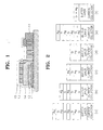
- FIGS. 2A through 2E An anode thin film according to a preferred embodiment of the present invention will now be described in more detail with reference to FIGS. 2A through 2E.
- the anode thin film according to the present invention includes a current collector and an anode active material provided on the current collector, the anode active material being formed of a multiple-layer thin film in which a Si layer and an Ag layer are stacked.
- the current collector is not specifically restricted but a copper film is generally used, the copper film being generally 100 to 300 nm in thickness.
- the anode active material layer shown in FIG. 2A is constructed of Si/Ag/Si/Ag/Si/Ag/Si/Ag layers sequentially stacked.
- the anode active material layer shown in FIG. 2B is constructed of Si/Ag/Si/Ag/Si/Ag layers sequentially stacked.
- the anode active material layer shown in FIG. 2C is constructed of Si/Ag/Si/Ag layers sequentially stacked.
- the anode active material layer shown in FIG. 2D is constructed of Si/Ag/Si layers sequentially stacked.
- the anode active material layer shown in FIG. 2E is constructed of Ag/Si/Ag/Si/Ag/Si/Ag layers sequentially stacked.
- the anode active material layer according to the present invention is preferably a multiple-layer structure in which Si layers and Ag layers are alternately stacked.
- the volumetric expansion of silicon can be more effectively suppressed by forming an Ag layer between Si layers.
- the thickness and number of stacked Si layers are proportional to the amount of the anode active material used. Thus, it is possible to change the thickness and number of stacked Si layers in various types according to device requirement and cathode capacity, preferably 50 to 250 ⁇ . If the thickness of stacked Si layers is less than 50 ⁇ , the number of Si/Ag multiple layers must be increased to meet the capacity as requested in design. An increase in the number of stacked Ag layers exceeding a predetermined range may increase an over-potential of the anode thin film. If the thickness of stacked Si layers is greater than 250 ⁇ , the volumetric expansion of silicon cannot sufficiently suppressed.
- silver (Ag) reacts with lithium at a low voltage range of 0.08 V or less to form a stable silver-lithium (Ag-Li) alloy.
- a lithium-silver (Li-Ag) alloy is slowly decomposed into Li and Ag so that reactant Li cannot completely escape from the alloy, which means lowered reversibility, thereby affecting irreversible capacity.
- Ag is deposited to a minimum thickness, preferably to a thickness of 10 to 70 ⁇ . If the thickness of Ag is less than 10 ⁇ , the effect of suppressing a volumetric change of Si is negligible. If the thickness of Ag is greater than 70 ⁇ , the rate of decomposition of the Li-Ag alloy into Li and Ag is undesirably reduced.
- the Si/Ag multiple-layer thin film stacked on the current collector can form a lithium secondary battery having various performances according to stacking sequence and thickness. If the topmost layer of the multiple-layer thin film is a Si layer, as shown in FIG. 2D, the battery exhibits excellent capacity. If the topmost layer of the multiple-layer thin film is an Ag layer, as shown in FIGS. 2A through C and FIG. 2E, the battery exhibits excellent cycle characteristics, which is because Ag in the topmost layer serves to suppress cracking due to volumetric expansion and shrinkage of Si and loss of a Si active material, at the interface between an electrode and an electrolyte.
- a single layer containing Si and Ag may be formed, unlike the Si/Ag multiple-layer thin film, as shown in FIGS. 2A through 2E.
- a buffer layer made of at least one selected from the group consisting of vanadium (V), nickel (Ni), molybdenum (Mo) and copper (Cu) may be further formed between the current collector and the anode active material layer.
- anode thin film of the present invention methods of forming a thin film of Si/Ag multiple layers or a single layer containing Si and Ag are not specifically restricted and sputtering, e-beam evaporation and/or ion beam assisted deposition (IBAD) may be used.
- IBAD ion beam assisted deposition
- a thin film having fine and uniform components and an amorphous or nano-particle structure according to the colling degree of a substrate on which thin films are formed can be attained.
- a mosaic sputtering method using a mosaic-shaped target a co-sputtering method using two or more targets or a sputtering method using an alloy target may be employed.
- thin films having various compositions can be attained by adjusting radio frequency (rf) power applied to each target.
- rf radio frequency
- the same deposition conditions for such as deposition pressure, gas flow rate, gas proportion or the like, are given.
- the only parameter is the rf power applied to each target in adjusting the composition of a thin film.
- the power for depositing a basic material, that is, silicon (Si) is maintained at an equal level, the levels of power for depositing additional materials are varied.
- the deposition power of Si is in the range of 100 to 300 W and the deposition power of metal (M) is in the range of 0 to 100 W.
- the parameter in varying the composition of a thin film is the number of chips.
- IBAD ion beam assisted deposition
- e-beams are simultaneously focused on different evaporation sources and evaporated to be co-sputtered on a substrate.
- composition of a thin film can be changed by adjusting the flux of e-beam, i.e., e-beam current, applied to each evaporation source. Also, the crystallinity and micro structure of the deposited thin film can be adjusted by changing the accelerated voltage of Ar ions.
- Si and Ag are co-sputtered to form a single layer containing Si and Ag.
- characteristics of a finally obtained anode active material layer may slightly differ according to the distribution, particle size and mixing ratio of silver distributed with silicon.
- the same effect as in the Si/Ag multiple-layer thin film, as shown in FIGS. 2A through 2E, can be attained by controlling micro-particle sized silver to be distributed uniformly among silicon particles.
- Si and Ag contained in the single layer are preferably mixed in a molar ratio of 7:3 to 3:7.
- the content of Ag relative to Si is greater than the above proportion, a large amount of Ag is present around Si that is reactive with Li, so that Si is shielded by Ag, prohibiting lithium from accessing to available silicon atoms, thereby leading to a considerably lower capacity of an electrode than designed. If the content of Ag relative to Si is less than the above proportion, the effect of suppressing a volumetric change of Si is undesirably negligible.
- the thickness of the single layer can be changed in various manners according to the requirement of a device and the capacity of a cathode. If it is possible to make fine particle-phase Ag be uniformly distributed among Si particles within the above range, the thickness of the single layer can be increased in an appropriate range.
- a buffer layer is preferably formed between the current collector and the anode active material layer.
- the buffer layer is preferably made of at least one selected from the group consisting of vanadium (V), nickel (Ni), molybdenum (Mo) and copper (Cu), and serves to relieve stress between the anode active material layer and the current collector and to ensure the stability of the interface therebetween and the interface between the anode active material layer and the electrolyte.
- the thickness of the buffer layer is preferably 50 to 250 ⁇ .
- the thickness of the buffer layer is less than 50 ⁇ , the buffering effect of the buffer layer, for example, relieved stress between the current collector and the anode active material layer, cannot sufficiently exhibited. If the thickness of the buffer layer is greater than 250 ⁇ , an increase in volume of the anode thin film is undesirably resulted, without a change in electrochemical property of the anode thin film.
- each thin film was sequentially deposited on a Cu substrate using 2-inch diameter Si, Ag and V targets, to prepare six anode thin films as listed in Table 1.
- an initial vacuum state was adjusted to 2 ⁇ 10 -6 torr, a V thin film was deposited to a thickness of 200 ⁇ with an rf power of 50 W under the conditions of argon (Ar) gas being induced to maintain an operating pressure of 5 mTorr and a flux of 10 sccm, and then an Ag thin film and a Si thin film were alternately deposited on the resultant.
- the Si thin film was deposited to a thickness of 70 to 200 ⁇ with rf power of 200 W
- the Ag thin film was deposited to a thickness of 25 to 50 ⁇ under the conditions of direct-current (dc) 270 V and 30 mA.
- a lithium secondary battery was fabricated using metallic lithium as a counter electrode and a reference electrode and using 1 M LiPF 6 dissolved in a mixed solvent of ethylene carbonate (EC) and diethylcarbonate (DEC) as an electrolyte solution.
- EC ethylene carbonate
- DEC diethylcarbonate
- a pure Si thin film was deposited on a Cu current collector to a thickness of 300 ⁇ using the same amount of Si as the total amount of Si used in sample MSA-2, thereby completing an anode thin film.
- a lithium secondary battery was fabricated using the anode thin film in the same manner as in Example 1.
- the cycle characteristics of the lithium secondary batteries employing the anode thin film prepared by Example 1 and the anode thin film prepared by Comparative Example 1 were evaluated, and the result thereof is shown in FIG. 3.
- the cycle characteristics were evaluated by performing more than 50 charging and discharging cycles on lithium with a current density of 50 ⁇ A/cm 2 within the range of measured potential of 0.08 to 1.5 V.
- the cycle characteristics of the anode active material layer of Example 1 were better than those of the Si single layer of Comparative Example 1.
- the anode active material layer of Example 1 showed greater than 95% of the initial capacity even after 50 cycles.
- the use of the Si/Ag multiple-layer thin film as an anode active material layer greatly reduces deterioration of an active material due to volumetric expansion or shrinkage of silicon, compared to the case of using the pure Si thin film (Comparative Example), leading to remarkable improvement of cycle characteristics.
- the cycle characteristics of the lithium secondary batteries employing the multiple-layer anode thin films having MSA-1, MSA-2 and MSA-4 structures of Example 1 were evaluated, and the result thereof is shown in FIG. 4.
- the cycle characteristics were evaluated by performing more than 100 charging and discharging cycles by a constant current method with a current density of 50 ⁇ A/cm 2 within the range of measured potential of 0.08 to 1.5 V versus Li.
- the thinner the Si layer the better the charging/discharging cycle characteristics.
- the MSA-4 anode thin film having a 200 ⁇ thick Si layer a reduction in capacity was observed after approximately 50 cycles.
- the MSA-1 and MSA-2 anode thin films respectively having 70 ⁇ and 100 ⁇ thick Si layers little reduction in capacity occurred even after 100 charging/discharging cycles.
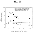
- FIGS. 5A and 5B the charge capacity, discharge capacity and irreversible capacity of the lithium secondary battery employing the multiple-layer thin film of Example 1 are shown in FIGS. 5A and 5B.
- these characteristics were evaluated under conditions in which charging and discharging were performed with a current density of 50 ⁇ A/cm 2 within the range of measured potential of 0.08 to 1.5 V.
- the irreversible capacity at the first cycle was maintained at a constant level irrespective of the amount of Si or Ag used as an active material. This result shows that the irreversible capacity at the first cycle is presumably caused by a side reaction occurring at the interface between an electrode and a liquid electrolyte, rather than by a structural damage of the active material itself.
- Si-Ag (Si 0.6 Ag 0.4 ) single layer having a stacked structure to a thickness of 900 ⁇ , as shown in FIG. 2F an anode thin film was fabricated in the same manner as in Example 1.
- rf power applied to the Si target was fixed to 200 W and dc voltages applied to the Ag target were varied.
- Cycle characteristics of lithium secondary batteries employing anode thin films prepared by Examples 2 through 5 were measured.
- the cycle characteristics were evaluated by performing more than 50 charging and discharging cycles on lithium by a constant current method with a current density of 50 ⁇ A/cm 2 within the range of measured potential of 0.12 to 1.5 V.
- the anode thin film according to the present invention can greatly improve cycle characteristics of a lithium secondary battery by suppressing volumetric expansion or shrinkage of silicon occurring during charging and discharging.
- the chemical and mechanical stability of the anode thin film can be greatly improved at an interface between an electrode and an electrolyte, thereby fabricating a lithium secondary battery having improved cycle characteristic.
Abstract
Description
- The present invention relates to an anode thin film for lithium secondary battery, and more particularly, to an anode thin film for a lithium secondary battery having improved charging/discharging cycle life characteristics by using silicon (Si) and silver (Ag) as materials of forming an anode active material layer formed on a current collector.
- Recently, according to advanced microelectronics industry and development of miniaturized, highly efficient electronic devices and very small sensor devices, small and thin batteries as power sources for driving such devices are highly demanded.
- FIG. 1 is a schematic diagram of a conventional thin film battery. Referring to FIG. 1, the thin film battery basically is constructed such that a
cathode 12, anelectrolyte 14 and ananode 13, each in the form of a thin film, are sequentially stacked on a current collector 11, to have the overall thickness of approximately 10 µm, characterized by the following advantages. - The thin-film stacked structure in which the anode is arranged in the vicinity of the cathode, increases a current density, leading to an excellent efficiency of a battery, and reduces moving distances of ions between the two electrodes, facilitating ionic mobility, by which the content of a reactive material can be greatly reduced. Also, since such thin film batteries can be easily fabricated in an arbitrary shape and size, they are expected to be used as promising main power sources for driving very small electronic device, MEMS (Micro Electro Mechanical System) and very small sensors.
- The thin film battery fabricated by the same process as in a semiconductor device can be mounted with an electronic circuit on a semiconductor chip, thereby implementing a CMOS (Complementary Metal Oxide Semiconductor) memory chip using the thin film battery as a back-up power source. Also, an unused space of an electronic device can be minimized, thereby maximizing the space utilization efficiency. Batteries having various voltages and capacities can be realized by serial/parallel connection through appropriate design and etching, leading to a variety of applications.
- Research into thin film batteries has hitherto focused on fabrication and evaluation of cathode thin films formed of V2O5, LiCoO2 or LiMn2O4, and satisfactory research achievements have been reported. Anode thin films for such batteries are mostly lithium thin films formed by deposition of lithium metal.
- Lithium metal having a relatively low melting point of approximately 180°C, is liable to be molten due to heat generated during soldering that is performed in a packaging process, which may cause damages to the device. Also, since lithium metal is highly reactive in the air, many handling difficulties are involved and an additional device for isolating the device from moisture and oxygen is necessary, which makes it difficult for lithium metal to be put into practical use as an electrode material of power source for driving very small electronic devices.
- Although the use of anode thin films of silicon-tin oxynitride (SITON), silicon dioxide (SnO2) or nitride as well as the lithium thin films have been attempted, irreversible reactions occurring during initial charging/discharging cycles are not properly controlled.
- To overcome the problem of a low charge/discharge efficiency of lithium, research into lithium alloy has been carried out. Much attention is being paid to a metal that can form lithium alloys, such as tin (Sn), silicon (Si) or aluminum (Al), as a next generation anode active material. While the anode active material exhibits excellent capacity characteristics with respect to lithium in a low voltage range, a change in volume of the active material due to intercalation/deintercalation of lithium during charging/discharging cycles, causes damages to an anode thin film structure, deteriorating cycle characteristics. In particular, in the thin film battery using a solid electrolyte, adhesion at the interface between an electrode and a current collector is considerably reduced, deteriorating the battery performance. Importantly, it is necessary to develop a material having excellent cycle characteristics without a reduction in capacity due to a irreversible reaction during intercalation or deintercalation of lithium.
- To solve the above-described problems, it is a first object of the present invention to provide an anode thin film for a lithium secondary battery having improved charging/discharging characteristics.
- To accomplish the object of the present invention, there is provided an anode thin film for a lithium secondary battery having a current collector and an anode active material layer formed thereon, wherein the anode active material layer is a multiple-layer thin film comprising a silicon (Si) layer and a silver (Ag) layer.
- Also, to accomplish the object of the present invention, there is provided an anode thin film for a lithium secondary battery having a current collector and an anode active material layer formed thereon, wherein the anode active material layer is a single-layer thin film comprising silicon (Si) and silver (Ag).
- The multiple-layer thin film layer comprises Si/Ag/Si layers, Si/Ag/Si/Ag layers, Si/Ag/Si/Ag/Si/Ag layers, Si/Ag/Si/Ag/Si/Ag/Si/Ag layers or Ag/Si/Ag/Si/Ag/Si/Ag layers.
- Also, In the anode thin film of the present invention, the topmost layer of the multiple-layer thin film layer is preferably formed of Ag. The lithium battery employing the anode thin film has a better cycle characteristics.
- In the anode thin film of the present invention, the Si layer and the Ag layer are alternately stacked. In particular, the Ag layer is formed between Si layers.
- The above objects and advantages of the present invention will become more apparent by describing in detail preferred embodiments thereof with reference to the attached drawings in which:
- FIG. 1 is a schematic diagram of a conventional thin film battery;
- FIG. 2 is a schematic diagram showing the structure of an anode employing a multiple-layer thin film prepared by Example 1 of the present invention;
- FIG. 3 is a diagram comparing cycle characteristics of lithium secondary batteries prepared by Example 1 of the present invention and Comparative Example 1;
- FIG. 4 is a diagram comparing cycle characteristics of anodes employing multiple-layer anode thin films having MSA-1, MSA-2 and MSA-4 structures, respectively, prepared by Example 1 of the present invention, depending on the thickness of a silicon (Si) layer;
- FIG. 5A is a diagram showing the charge capacity, discharge capacity and irreversible capacity of an anode employing the multiple-layer thin film prepared by Example 1 of the present invention during the first charge/discharge cycle, depending on the total thickness of a silicon (Si) layer;
- FIG. 5B is a diagram showing the charge capacity, discharge capacity and irreversible capacity of an anode employing the multiple-layer thin film prepared by Example 1 of the present invention during the first charge/discharge cycle, depending on the total thickness of a silver (Ag) layer;
- FIG. 6 is a diagram comparing cycle characteristics of anodes employing multiple-layer anode thin films having MSA-1 and MSA-6 structures, respectively, prepared by Example 1 of the present invention, depending on the thickness of a silver (Ag) layer;
- FIG. 7 is a diagram comparing cycle characteristics of anodes employing multiple-layer anode thin films having MSA-4 and MSA-5 structures, respectively, prepared by Example 1 of the present invention; and
- FIG. 8 is a graph showing cycle characteristics of anodes employing a silicon-silver single layer anode thin film prepared by Example 2 of the present invention.
-
- Although silicon has a relatively large capacity with respect to lithium even at a low voltage range so that it can be advantageously used as an anode active material, it cannot properly suppress deterioration of an active material due to a great change in volume occurring during charging and discharging, leading to limited application of silicon as an anode active material. The present invention is characterized in that an anode active material layer is formed using both silicon and silver (Ag) that can be functioned as a medium for lithium ions and electron movement while solving such a drawback of silicon, that is, stress due to volumetric expansion of silicon. Here, since silver does not react with silicon, the capacity and reversibility in a lithium-silicon reaction can be ensured. Also, the structural stability of an active material can be ensured during a subsequent heating step that is required in a packaging process of a thin film battery. In a lithium secondary battery employing such an anode active material layer, various charging/discharging cycle characteristics can be attained through control of the micro structure, crystallinity, size and distribution of each material for silicon and silver layers by thickness of each of silicon (Si) and silver (Ag) layers and sequence of the layers, overall thickness of the anode active material layer, thermal treatment conditions for forming a thin film, a mixture ratio of Ag and Si, and the like.
- An anode thin film according to a preferred embodiment of the present invention will now be described in more detail with reference to FIGS. 2A through 2E.
- As shown in FIGS. 2A through 2E, the anode thin film according to the present invention includes a current collector and an anode active material provided on the current collector, the anode active material being formed of a multiple-layer thin film in which a Si layer and an Ag layer are stacked.
- In the anode thin film according to the present invention, the current collector is not specifically restricted but a copper film is generally used, the copper film being generally 100 to 300 nm in thickness.
- The anode active material layer shown in FIG. 2A is constructed of Si/Ag/Si/Ag/Si/Ag/Si/Ag layers sequentially stacked. The anode active material layer shown in FIG. 2B is constructed of Si/Ag/Si/Ag/Si/Ag layers sequentially stacked. The anode active material layer shown in FIG. 2C is constructed of Si/Ag/Si/Ag layers sequentially stacked. The anode active material layer shown in FIG. 2D is constructed of Si/Ag/Si layers sequentially stacked. The anode active material layer shown in FIG. 2E is constructed of Ag/Si/Ag/Si/Ag/Si/Ag layers sequentially stacked.
- As shown in FIGS. 2A through 2E, the anode active material layer according to the present invention is preferably a multiple-layer structure in which Si layers and Ag layers are alternately stacked. In particular, the volumetric expansion of silicon can be more effectively suppressed by forming an Ag layer between Si layers.
- The thickness and number of stacked Si layers are proportional to the amount of the anode active material used. Thus, it is possible to change the thickness and number of stacked Si layers in various types according to device requirement and cathode capacity, preferably 50 to 250 Å. If the thickness of stacked Si layers is less than 50 Å, the number of Si/Ag multiple layers must be increased to meet the capacity as requested in design. An increase in the number of stacked Ag layers exceeding a predetermined range may increase an over-potential of the anode thin film. If the thickness of stacked Si layers is greater than 250 Å, the volumetric expansion of silicon cannot sufficiently suppressed.
- On the other hand, silver (Ag) reacts with lithium at a low voltage range of 0.08 V or less to form a stable silver-lithium (Ag-Li) alloy. However, during charging, a lithium-silver (Li-Ag) alloy is slowly decomposed into Li and Ag so that reactant Li cannot completely escape from the alloy, which means lowered reversibility, thereby affecting irreversible capacity. Thus, in order to allow Ag to be served as such, Ag is deposited to a minimum thickness, preferably to a thickness of 10 to 70 Å. If the thickness of Ag is less than 10 Å, the effect of suppressing a volumetric change of Si is negligible. If the thickness of Ag is greater than 70 Å, the rate of decomposition of the Li-Ag alloy into Li and Ag is undesirably reduced.
- The Si/Ag multiple-layer thin film stacked on the current collector can form a lithium secondary battery having various performances according to stacking sequence and thickness. If the topmost layer of the multiple-layer thin film is a Si layer, as shown in FIG. 2D, the battery exhibits excellent capacity. If the topmost layer of the multiple-layer thin film is an Ag layer, as shown in FIGS. 2A through C and FIG. 2E, the battery exhibits excellent cycle characteristics, which is because Ag in the topmost layer serves to suppress cracking due to volumetric expansion and shrinkage of Si and loss of a Si active material, at the interface between an electrode and an electrolyte.
- Also, in the anode thin film of the present invention, a single layer containing Si and Ag, as shown in FIG. 2F, may be formed, unlike the Si/Ag multiple-layer thin film, as shown in FIGS. 2A through 2E. Here, a buffer layer made of at least one selected from the group consisting of vanadium (V), nickel (Ni), molybdenum (Mo) and copper (Cu) may be further formed between the current collector and the anode active material layer.
- In the anode thin film of the present invention, methods of forming a thin film of Si/Ag multiple layers or a single layer containing Si and Ag are not specifically restricted and sputtering, e-beam evaporation and/or ion beam assisted deposition (IBAD) may be used. Here, the processing conditions of each method are not specifically restricted but will now be explained briefly.
- According to the sputtering method, a thin film having fine and uniform components and an amorphous or nano-particle structure according to the colling degree of a substrate on which thin films are formed, can be attained. In order to manufacture a thin film having a multiple-component system, a mosaic sputtering method using a mosaic-shaped target, a co-sputtering method using two or more targets or a sputtering method using an alloy target may be employed.
- Specifically, according to the co-sputtering method in which separate targets are simultaneously sputtered for deposition, thin films having various compositions can be attained by adjusting radio frequency (rf) power applied to each target. During the co-sputtering method, the same deposition conditions for such as deposition pressure, gas flow rate, gas proportion or the like, are given. Thus, the only parameter is the rf power applied to each target in adjusting the composition of a thin film. Generally, while the power for depositing a basic material, that is, silicon (Si), is maintained at an equal level, the levels of power for depositing additional materials are varied. For example, the deposition power of Si is in the range of 100 to 300 W and the deposition power of metal (M) is in the range of 0 to 100 W. In the case of the mosaic sputtering method, under the same processing conditions, the parameter in varying the composition of a thin film is the number of chips.
- The use of ion beam assisted deposition (IBAD) makes it possible to prepare a multiple-component, amorphous or crystalline thin film by appropriately adjusting ion beam conditions using the mobility and reactivity of atoms which are increased while accelerated electron beams collide with atoms deposited on a substrate. The composition of the thin film can be changed by adjusting the current of ion beams applied to each evaporation source. The crystallinity and micro structure of the deposited thin film can be adjusted by changing the flux and accelerated voltage of Ar ions.
- According to the e-beam evaporation method, e-beams are simultaneously focused on different evaporation sources and evaporated to be co-sputtered on a substrate.
- The composition of a thin film can be changed by adjusting the flux of e-beam, i.e., e-beam current, applied to each evaporation source. Also, the crystallinity and micro structure of the deposited thin film can be adjusted by changing the accelerated voltage of Ar ions.
- In the present invention, Si and Ag are co-sputtered to form a single layer containing Si and Ag. When the single layer is formed in the above-described co-sputtering method, characteristics of a finally obtained anode active material layer may slightly differ according to the distribution, particle size and mixing ratio of silver distributed with silicon. However, the same effect as in the Si/Ag multiple-layer thin film, as shown in FIGS. 2A through 2E, can be attained by controlling micro-particle sized silver to be distributed uniformly among silicon particles. Here, Si and Ag contained in the single layer are preferably mixed in a molar ratio of 7:3 to 3:7. If the content of Ag relative to Si is greater than the above proportion, a large amount of Ag is present around Si that is reactive with Li, so that Si is shielded by Ag, prohibiting lithium from accessing to available silicon atoms, thereby leading to a considerably lower capacity of an electrode than designed. If the content of Ag relative to Si is less than the above proportion, the effect of suppressing a volumetric change of Si is undesirably negligible. The thickness of the single layer can be changed in various manners according to the requirement of a device and the capacity of a cathode. If it is possible to make fine particle-phase Ag be uniformly distributed among Si particles within the above range, the thickness of the single layer can be increased in an appropriate range.
- In the anode thin film of the present invention, as shown in FIGS. 2A through 2F, a buffer layer is preferably formed between the current collector and the anode active material layer. The buffer layer is preferably made of at least one selected from the group consisting of vanadium (V), nickel (Ni), molybdenum (Mo) and copper (Cu), and serves to relieve stress between the anode active material layer and the current collector and to ensure the stability of the interface therebetween and the interface between the anode active material layer and the electrolyte. Here, the thickness of the buffer layer is preferably 50 to 250 Å. If the thickness of the buffer layer is less than 50 Å, the buffering effect of the buffer layer, for example, relieved stress between the current collector and the anode active material layer, cannot sufficiently exhibited. If the thickness of the buffer layer is greater than 250 Å, an increase in volume of the anode thin film is undesirably resulted, without a change in electrochemical property of the anode thin film.
- The present invention will now be described in more detail through the following examples, but not limited thereto.
- The respective components of each thin film were sequentially deposited on a Cu substrate using 2-inch diameter Si, Ag and V targets, to prepare six anode thin films as listed in Table 1.
- At the time of deposition, an initial vacuum state was adjusted to 2×10⁻⁶ torr, a V thin film was deposited to a thickness of 200 Å with an rf power of 50 W under the conditions of argon (Ar) gas being induced to maintain an operating pressure of 5 mTorr and a flux of 10 sccm, and then an Ag thin film and a Si thin film were alternately deposited on the resultant. Here, the Si thin film was deposited to a thickness of 70 to 200 Å with rf power of 200 W, and the Ag thin film was deposited to a thickness of 25 to 50 Å under the conditions of direct-current (dc) 270 V and 30 mA.
Sample Structure of anode active material layers stacked Thickness of Si layer (Å) Thickness of Ag layer (Å) MSA-1 Cu/V(200Å)/Si/Ag/Si/Ag/Si/Ag/Si/ Ag 70 25 MSA-2 Cu/V(200Å)/Si/Ag/Si/Ag/Si/ Ag 100 25 MSA-3 Cu/V(200Å)/Ag/Si/Ag/Si/Ag/Si/ Ag 100 25 MSA-4 Cu/V(200Å)/Si/Ag/Si/ Ag 200 25 MSA-5 Cu/V(200Å)/Si/Ag/ Si 200 25 MSA-6 Cu/V(200Å)/Si/Ag/Si/Ag/Si/Ag/Si/ Ag 70 50 - In order to evaluate electrochemical properties of anode thin films manufactured by the above-described procedure, a lithium secondary battery was fabricated using metallic lithium as a counter electrode and a reference electrode and using 1 M LiPF6 dissolved in a mixed solvent of ethylene carbonate (EC) and diethylcarbonate (DEC) as an electrolyte solution.
- A pure Si thin film was deposited on a Cu current collector to a thickness of 300 Å using the same amount of Si as the total amount of Si used in sample MSA-2, thereby completing an anode thin film. A lithium secondary battery was fabricated using the anode thin film in the same manner as in Example 1.
- The cycle characteristics of the lithium secondary batteries employing the anode thin film prepared by Example 1 and the anode thin film prepared by Comparative Example 1 were evaluated, and the result thereof is shown in FIG. 3. Here, the cycle characteristics were evaluated by performing more than 50 charging and discharging cycles on lithium with a current density of 50 µA/cm2 within the range of measured potential of 0.08 to 1.5 V.
- Referring to FIG. 3, the cycle characteristics of the anode active material layer of Example 1 were better than those of the Si single layer of Comparative Example 1. In particular, the anode active material layer of Example 1 showed greater than 95% of the initial capacity even after 50 cycles. As described above, the use of the Si/Ag multiple-layer thin film as an anode active material layer greatly reduces deterioration of an active material due to volumetric expansion or shrinkage of silicon, compared to the case of using the pure Si thin film (Comparative Example), leading to remarkable improvement of cycle characteristics.
- The cycle characteristics of the lithium secondary batteries employing the multiple-layer anode thin films having MSA-1, MSA-2 and MSA-4 structures of Example 1 were evaluated, and the result thereof is shown in FIG. 4. Here, the cycle characteristics were evaluated by performing more than 100 charging and discharging cycles by a constant current method with a current density of 50 µA/cm2 within the range of measured potential of 0.08 to 1.5 V versus Li. Referring to FIG. 4, the thinner the Si layer, the better the charging/discharging cycle characteristics. In the MSA-4 anode thin film having a 200 Å thick Si layer, a reduction in capacity was observed after approximately 50 cycles. In the MSA-1 and MSA-2 anode thin films respectively having 70 Å and 100 Å thick Si layers, little reduction in capacity occurred even after 100 charging/discharging cycles.
- Referring to FIGS. 3 and 4, irreversible capacity was observed during the first cycle.
- In order to verify causes of such irreversible capacity, the charge capacity, discharge capacity and irreversible capacity of the lithium secondary battery employing the multiple-layer thin film of Example 1 are shown in FIGS. 5A and 5B. Here, these characteristics were evaluated under conditions in which charging and discharging were performed with a current density of 50 µA/cm2 within the range of measured potential of 0.08 to 1.5 V.
- Referring to FIGS. 5A and 5B, while the charge capacity and discharge capacity at the first cycle were proportional to the amount of a Si active material, the irreversible capacity was maintained at a constant level irrespective of the amount of Si or Ag used as an active material. This result shows that the irreversible capacity at the first cycle is presumably caused by a side reaction occurring at the interface between an electrode and a liquid electrolyte, rather than by a structural damage of the active material itself.
- In order to evaluate cycle characteristics depending on the thickness of an Ag layer of Example 1, cycle characteristics of lithium secondary batteries employing anode thin films having MSA-1 and MSA-6 structures were investigated, and the result thereof is shown in FIG. 6. Both of the lithium secondary batteries employing anode thin films having MSA-1 and MSA-6 structures exhibit excellent cycle characteristics. In particular, as the thickness of the Ag layer increased to 50 Å as in the MSA-6 structure, the capacity decreased less sharply over repeated cycles than in the MSA-1 structure in which the thickness of the Ag layer is 25 Å. Also, approximately 95% of the initial charge capacity of 18 µAh was maintained even after 100 cycles.
- In order to compare cases where the topmost layer of an anode active material layer is an Ag layer and the topmost layer of anode active material layer is a Si layer, cycle characteristics of lithium secondary batteries employing multiple-layer thin films having MSA-4 and MSA-5 structures were measured, and the result thereof is shown in FIG. 7.
- Referring to FIG. 7, when Si is present in the topmost layer of the anode active material layer as in the MSA-5 structure, a larger capacity was exhibited than in the case when Ag is present in the topmost layer of the anode active material layer as in the MSA-4. Also, the MSA-4 structure showed better cycle characteristics than the MSA-5 structure in which Si is exposed to an electrolyte solution. This is because the Ag layer present in the topmost layer can suppress cracking due to volumetric expansion or shrinkage of silicon and a loss of an active material at the interface between the electrolyte and electrode. This result suggests that a lithium secondary battery employing a solid electrolyte can greatly improve chemical and mechanical stability between an electrode and an electrolyte by forming an Ag layer in the topmost layer of the anode active material layer.
- Except that Si, Ag and V targets as anode thin films were co-sputtered to deposit a Si-Ag (Si0.6Ag0.4) single layer having a stacked structure to a thickness of 900 Å, as shown in FIG. 2F, an anode thin film was fabricated in the same manner as in Example 1. Here, in order to adjust the contents of Si and Ag in the single layer, rf power applied to the Si target was fixed to 200 W and dc voltages applied to the Ag target were varied.
- Except that a Ni target was used instead of the V target, an anode thin film was fabricated in the same manner as in Example 1.
- Except that a Mo target was used instead of the V target, an anode thin film was fabricated in the same manner as in Example 1.
- Except that a Cu target was used instead of the V target, an anode thin film was fabricated in the same manner as in Example 1.
- Cycle characteristics of lithium secondary batteries employing anode thin films prepared by Examples 2 through 5 were measured. Here, the cycle characteristics were evaluated by performing more than 50 charging and discharging cycles on lithium by a constant current method with a current density of 50 µA/cm2 within the range of measured potential of 0.12 to 1.5 V.
- The evaluation result showed that the cycle characteristics of the lithium secondary batteries prepared by Examples 2 through 5 were relatively good. Referring to FIG. 8 showing the case of Example 2, in particular, approximately 90% of the initial charge capacity of 32 µAh was maintained even after 50 cycles.
- As described above, the anode thin film according to the present invention can greatly improve cycle characteristics of a lithium secondary battery by suppressing volumetric expansion or shrinkage of silicon occurring during charging and discharging. Thus, the chemical and mechanical stability of the anode thin film can be greatly improved at an interface between an electrode and an electrolyte, thereby fabricating a lithium secondary battery having improved cycle characteristic.
- Although the invention has been described in detailed embodiments, it is not intended that the scope of the claims appended hereto be limited to the description as set forth herein. Accordingly, it is understood that various other modifications will be apparent to and can be readily made by those skilled in the art without departing from the scope and spirit of this invention.
Claims (9)
- An anode thin film for a lithium secondary battery having a current collector and an anode active material layer formed thereon,
characterized in that
the anode active material layer is a multiple-layer thin film comprising at least one silicon (Si) layer and at least one silver (Ag) layer. - The anode thin film of claim 1, wherein the thickness of the respective Si layer is in the range of 50 to 250 Å and the thickness of the respective Ag layer is in the range of 10 to 70 Å.
- The anode thin film of claim 1 or 2, wherein the Si and Ag layers are alternately stacked.
- The anode thin film of claim 3, wherein at least one Ag layer is formed between Si layers.
- The anode thin film of any one of claims 1 to 4, wherein the topmost layer of the multiple-layer thin film is made of Ag.
- An anode thin film for a lithium secondary battery having a current collector and an anode active material layer formed thereon,
characterized in that
the anode active material layer is a single-layer thin film comprising silicon (Si) and silver (Ag). - The anode thin film of claim 6, wherein Si and Ag comprised in the single layer are mixed in a molar ratio of 7:3 to 3:7.
- The anode thin film of any one of claims 1 to 7, further comprising a buffer layer between the current collector and the anode active material layer, the buffer layer being made of at least one selected from the group consisting of vanadium (V), nickel (Ni), molybdenum (Mo) and copper (Cu).
- The anode thin film of claim 8, wherein the thickness of the buffer layer is in the range of 50 to 250 Å.
Applications Claiming Priority (4)
| Application Number | Priority Date | Filing Date | Title |
|---|---|---|---|
| KR2000068728 | 2000-11-18 | ||
| KR20000068728 | 2000-11-18 | ||
| KR10-2001-0052112A KR100389908B1 (en) | 2000-11-18 | 2001-08-28 | Anode thin film for Lithium secondary battery |
| KR2001052112 | 2001-08-28 |
Publications (4)
| Publication Number | Publication Date |
|---|---|
| EP1207566A2 true EP1207566A2 (en) | 2002-05-22 |
| EP1207566A3 EP1207566A3 (en) | 2004-01-21 |
| EP1207566B1 EP1207566B1 (en) | 2007-03-07 |
| EP1207566B8 EP1207566B8 (en) | 2007-09-12 |
Family
ID=26638547
Family Applications (1)
| Application Number | Title | Priority Date | Filing Date |
|---|---|---|---|
| EP01126821A Expired - Lifetime EP1207566B8 (en) | 2000-11-18 | 2001-11-10 | Anode thin film for lithium secondary battery |
Country Status (5)
| Country | Link |
|---|---|
| US (1) | US6828063B2 (en) |
| EP (1) | EP1207566B8 (en) |
| JP (1) | JP3581124B2 (en) |
| AT (1) | ATE356444T1 (en) |
| DE (1) | DE60129196T2 (en) |
Cited By (2)
| Publication number | Priority date | Publication date | Assignee | Title |
|---|---|---|---|---|
| EP1289045A2 (en) * | 2001-08-25 | 2003-03-05 | Samsung SDI Co. Ltd. | Thin film for anode of lithium secondary battery and manufacturing method thereof |
| CN103144393A (en) * | 2013-04-02 | 2013-06-12 | 南开大学 | Silicon-based thin film material with sandwich structure and preparation method and application thereof |
Families Citing this family (43)
| Publication number | Priority date | Publication date | Assignee | Title |
|---|---|---|---|---|
| US6844113B2 (en) * | 2001-04-13 | 2005-01-18 | Sanyo Electric Co., Ltd. | Electrode for lithium secondary battery and method for producing the same |
| US8236443B2 (en) | 2002-08-09 | 2012-08-07 | Infinite Power Solutions, Inc. | Metal film encapsulation |
| US8021778B2 (en) | 2002-08-09 | 2011-09-20 | Infinite Power Solutions, Inc. | Electrochemical apparatus with barrier layer protected substrate |
| US8404376B2 (en) | 2002-08-09 | 2013-03-26 | Infinite Power Solutions, Inc. | Metal film encapsulation |
| US20070264564A1 (en) | 2006-03-16 | 2007-11-15 | Infinite Power Solutions, Inc. | Thin film battery on an integrated circuit or circuit board and method thereof |
| US8431264B2 (en) | 2002-08-09 | 2013-04-30 | Infinite Power Solutions, Inc. | Hybrid thin-film battery |
| US8394522B2 (en) | 2002-08-09 | 2013-03-12 | Infinite Power Solutions, Inc. | Robust metal film encapsulation |
| US8445130B2 (en) | 2002-08-09 | 2013-05-21 | Infinite Power Solutions, Inc. | Hybrid thin-film battery |
| US8535396B2 (en) | 2002-08-09 | 2013-09-17 | Infinite Power Solutions, Inc. | Electrochemical apparatus with barrier layer protected substrate |
| WO2004025757A2 (en) * | 2002-09-10 | 2004-03-25 | California Institute Of Technology | High-capacity nanostructured silicon and lithium alloys thereof |
| US8728285B2 (en) | 2003-05-23 | 2014-05-20 | Demaray, Llc | Transparent conductive oxides |
| JP3746499B2 (en) * | 2003-08-22 | 2006-02-15 | 三星エスディアイ株式会社 | Negative electrode active material for lithium secondary battery, method for producing the same, and lithium secondary battery |
| US20050074672A1 (en) * | 2003-10-01 | 2005-04-07 | Keiko Matsubara | Negative active material for rechargeable lithium battery, method of preparing same and rechargeable lithium battery using same |
| US7816032B2 (en) * | 2003-11-28 | 2010-10-19 | Panasonic Corporation | Energy device and method for producing the same |
| US7781102B2 (en) * | 2004-04-22 | 2010-08-24 | California Institute Of Technology | High-capacity nanostructured germanium-containing materials and lithium alloys thereof |
| WO2006063308A2 (en) | 2004-12-08 | 2006-06-15 | Symmorphix, Inc. | DEPOSITION OF LICoO2 |
| US7959769B2 (en) | 2004-12-08 | 2011-06-14 | Infinite Power Solutions, Inc. | Deposition of LiCoO2 |
| JP5039956B2 (en) * | 2006-09-07 | 2012-10-03 | トヨタ自動車株式会社 | Negative electrode active material, negative electrode and lithium secondary battery |
| KR20090069323A (en) | 2006-09-29 | 2009-06-30 | 인피니트 파워 솔루션스, 인크. | Masking of and material constraint for depositing battery layers on flexible substrates |
| US8197781B2 (en) | 2006-11-07 | 2012-06-12 | Infinite Power Solutions, Inc. | Sputtering target of Li3PO4 and method for producing same |
| CN101903560B (en) | 2007-12-21 | 2014-08-06 | 无穷动力解决方案股份有限公司 | Method for sputter targets for electrolyte films |
| US8268488B2 (en) | 2007-12-21 | 2012-09-18 | Infinite Power Solutions, Inc. | Thin film electrolyte for thin film batteries |
| EP2229706B1 (en) | 2008-01-11 | 2014-12-24 | Infinite Power Solutions, Inc. | Thin film encapsulation for thin film batteries and other devices |
| JP5595377B2 (en) | 2008-04-02 | 2014-09-24 | インフィニット パワー ソリューションズ, インコーポレイテッド | Control and protection of passive over and under voltage for energy storage devices associated with energy intake |
| JP2012500610A (en) | 2008-08-11 | 2012-01-05 | インフィニット パワー ソリューションズ, インコーポレイテッド | Energy device with integrated collector surface and method for electromagnetic energy acquisition |
| KR101613671B1 (en) | 2008-09-12 | 2016-04-19 | 사푸라스트 리써치 엘엘씨 | Energy device with integral conductive surface for data communication via electromagnetic energy and method thereof |
| US8508193B2 (en) | 2008-10-08 | 2013-08-13 | Infinite Power Solutions, Inc. | Environmentally-powered wireless sensor module |
| JP5181002B2 (en) * | 2009-08-21 | 2013-04-10 | 尾池工業株式会社 | Scale-like thin film fine powder dispersion or scale-like thin film fine powder, paste using the same, battery electrode, and lithium secondary battery |
| KR101792287B1 (en) | 2009-09-01 | 2017-10-31 | 사푸라스트 리써치 엘엘씨 | Printed circuit board with integrated thin film battery |
| CN102208617B (en) * | 2010-03-31 | 2013-10-30 | 比亚迪股份有限公司 | Method for preparing cathode active substance of lithium ion secondary cells |
| CN102947976B (en) | 2010-06-07 | 2018-03-16 | 萨普拉斯特研究有限责任公司 | Chargeable, highdensity electrochemical apparatus |
| JP5640587B2 (en) * | 2010-09-08 | 2014-12-17 | ソニー株式会社 | Solid electrolyte battery |
| CN103238240B (en) * | 2010-12-07 | 2016-05-18 | 株式会社半导体能源研究所 | Electrical storage device |
| JP6035013B2 (en) | 2011-08-30 | 2016-11-30 | 株式会社半導体エネルギー研究所 | Electrode fabrication method |
| JP2013054878A (en) | 2011-09-02 | 2013-03-21 | Semiconductor Energy Lab Co Ltd | Method of manufacturing electrode and power storage device |
| KR101368323B1 (en) * | 2011-12-16 | 2014-02-28 | 지에스에너지 주식회사 | Thin film battery with improved performance by surface treatment and method of manufacturing the thin film battery |
| US9384904B2 (en) | 2012-04-06 | 2016-07-05 | Semiconductor Energy Laboratory Co., Ltd. | Negative electrode for power storage device, method for forming the same, and power storage device |
| JP6216154B2 (en) | 2012-06-01 | 2017-10-18 | 株式会社半導体エネルギー研究所 | Negative electrode for power storage device and power storage device |
| US8810294B2 (en) * | 2012-10-10 | 2014-08-19 | Texas Instruments Incorporated | Balanced auxiliary on time generator for multiphase stackable constant on time control architecture |
| KR102195511B1 (en) | 2012-11-07 | 2020-12-28 | 가부시키가이샤 한도오따이 에네루기 켄큐쇼 | Electrode for power storage device, power storage device, and manufacturing method of electrode for power storage device |
| US9478797B2 (en) * | 2013-01-25 | 2016-10-25 | Applejack 199 L.P. | System, method and apparatus for forming a thin film lithium ion battery |
| CN111640913B (en) * | 2019-03-01 | 2021-08-06 | 宁德时代新能源科技股份有限公司 | Negative plate and secondary battery |
| CN110783556A (en) * | 2019-10-09 | 2020-02-11 | 桂林电子科技大学 | Composite three-dimensional composite structure film and preparation method and application thereof |
Citations (4)
| Publication number | Priority date | Publication date | Assignee | Title |
|---|---|---|---|---|
| JPH0722017A (en) * | 1993-07-06 | 1995-01-24 | Mitsubishi Cable Ind Ltd | Alloy for lithium secondary battery negative electrode and lithium secondary battery provided with negative electrode made of this alloy |
| EP0668621A1 (en) * | 1994-02-22 | 1995-08-23 | Mitsubishi Cable Industries, Ltd. | Alloy for negative electrode of lithium secondary battery and lithium secondary battery |
| EP0690517A1 (en) * | 1994-05-30 | 1996-01-03 | Canon Kabushiki Kaisha | rechargeable lithium battery |
| EP0872902A1 (en) * | 1997-04-14 | 1998-10-21 | Hydro-Quebec | Dense alloyed anode metal sheet with internal stress compensation |
Family Cites Families (3)
| Publication number | Priority date | Publication date | Assignee | Title |
|---|---|---|---|---|
| JP3116857B2 (en) | 1997-04-04 | 2000-12-11 | 日本電気株式会社 | Rechargeable battery mounted on semiconductor substrate |
| US6235427B1 (en) * | 1998-05-13 | 2001-05-22 | Fuji Photo Film Co., Ltd. | Nonaqueous secondary battery containing silicic material |
| JP4728458B2 (en) | 1998-06-12 | 2011-07-20 | 宇部興産株式会社 | Non-aqueous secondary battery |
-
2001
- 2001-11-10 AT AT01126821T patent/ATE356444T1/en not_active IP Right Cessation
- 2001-11-10 EP EP01126821A patent/EP1207566B8/en not_active Expired - Lifetime
- 2001-11-10 DE DE60129196T patent/DE60129196T2/en not_active Expired - Lifetime
- 2001-11-16 US US09/987,939 patent/US6828063B2/en not_active Expired - Fee Related
- 2001-11-19 JP JP2001353330A patent/JP3581124B2/en not_active Expired - Fee Related
Patent Citations (4)
| Publication number | Priority date | Publication date | Assignee | Title |
|---|---|---|---|---|
| JPH0722017A (en) * | 1993-07-06 | 1995-01-24 | Mitsubishi Cable Ind Ltd | Alloy for lithium secondary battery negative electrode and lithium secondary battery provided with negative electrode made of this alloy |
| EP0668621A1 (en) * | 1994-02-22 | 1995-08-23 | Mitsubishi Cable Industries, Ltd. | Alloy for negative electrode of lithium secondary battery and lithium secondary battery |
| EP0690517A1 (en) * | 1994-05-30 | 1996-01-03 | Canon Kabushiki Kaisha | rechargeable lithium battery |
| EP0872902A1 (en) * | 1997-04-14 | 1998-10-21 | Hydro-Quebec | Dense alloyed anode metal sheet with internal stress compensation |
Cited By (6)
| Publication number | Priority date | Publication date | Assignee | Title |
|---|---|---|---|---|
| EP1289045A2 (en) * | 2001-08-25 | 2003-03-05 | Samsung SDI Co. Ltd. | Thin film for anode of lithium secondary battery and manufacturing method thereof |
| EP1289045A3 (en) * | 2001-08-25 | 2004-03-03 | Samsung SDI Co. Ltd. | Thin film for anode of lithium secondary battery and manufacturing method thereof |
| US6824922B2 (en) | 2001-08-25 | 2004-11-30 | Samsung Sdi Co., Ltd. | Thin film for anode of lithium secondary battery and manufacturing method thereof |
| US7316867B2 (en) | 2001-08-25 | 2008-01-08 | Samsung Sdi Co., Ltd. | Method for manufacturing a multi-layered thin film for use as an anode in a lithium secondary battery |
| CN103144393A (en) * | 2013-04-02 | 2013-06-12 | 南开大学 | Silicon-based thin film material with sandwich structure and preparation method and application thereof |
| CN103144393B (en) * | 2013-04-02 | 2015-06-17 | 南开大学 | Silicon-based thin film material with sandwich structure and preparation method and application thereof |
Also Published As
| Publication number | Publication date |
|---|---|
| EP1207566B1 (en) | 2007-03-07 |
| DE60129196T2 (en) | 2007-10-11 |
| JP2002198037A (en) | 2002-07-12 |
| EP1207566A3 (en) | 2004-01-21 |
| US20020048705A1 (en) | 2002-04-25 |
| US6828063B2 (en) | 2004-12-07 |
| DE60129196D1 (en) | 2007-08-16 |
| ATE356444T1 (en) | 2007-03-15 |
| JP3581124B2 (en) | 2004-10-27 |
| EP1207566B8 (en) | 2007-09-12 |
Similar Documents
| Publication | Publication Date | Title |
|---|---|---|
| US6828063B2 (en) | Anode thin film for lithium secondary battery | |
| US6824922B2 (en) | Thin film for anode of lithium secondary battery and manufacturing method thereof | |
| KR100389908B1 (en) | Anode thin film for Lithium secondary battery | |
| US6168884B1 (en) | Battery with an in-situ activation plated lithium anode | |
| JP4415241B2 (en) | Negative electrode for secondary battery, secondary battery using the same, and method for producing negative electrode | |
| US20040048157A1 (en) | Lithium vanadium oxide thin-film battery | |
| US20230246163A1 (en) | Surface protection of lithium metal anode | |
| US11876231B2 (en) | Diffusion barrier films enabling the stability of lithium | |
| JP2002520783A (en) | Electrode material and composition containing the same | |
| WO2005076389A9 (en) | Self-contained, alloy type, thin film anodes for lithium-ion batteries | |
| EP1289033B1 (en) | Anode thin film for lithium secondary battery and preparation method thereof | |
| US6979516B2 (en) | Lithium secondary battery and positive electrode for lithium secondary battery | |
| KR100563081B1 (en) | Thin negative electrode for lithium secondary battery and manufacturing method thereof | |
| KR100495674B1 (en) | A cathode thin film for all solid state battery, preparation method thereof, and lithium thin film battery using the same | |
| JPWO2005008809A1 (en) | Anode for non-aqueous electrolyte secondary battery and non-aqueous electrolyte secondary battery | |
| CN115552662A (en) | Battery and method for manufacturing same | |
| KR20050031162A (en) | Negative active material for lithium secondary battery and lithium secondary battery comprising same |
Legal Events
| Date | Code | Title | Description |
|---|---|---|---|
| PUAI | Public reference made under article 153(3) epc to a published international application that has entered the european phase |
Free format text: ORIGINAL CODE: 0009012 |
|
| AX | Request for extension of the european patent |
Free format text: AL;LT;LV;MK;RO;SI |
|
| PUAL | Search report despatched |
Free format text: ORIGINAL CODE: 0009013 |
|
| AK | Designated contracting states |
Kind code of ref document: A3 Designated state(s): AT BE CH CY DE DK ES FI FR GB GR IE IT LI LU MC NL PT SE TR |
|
| AX | Request for extension of the european patent |
Extension state: AL LT LV MK RO SI |
|
| 17P | Request for examination filed |
Effective date: 20040714 |
|
| 17Q | First examination report despatched |
Effective date: 20040831 |
|
| AKX | Designation fees paid |
Designated state(s): AT BE CH LI |
|
| REG | Reference to a national code |
Ref country code: DE Ref legal event code: 8566 |
|
| GRAP | Despatch of communication of intention to grant a patent |
Free format text: ORIGINAL CODE: EPIDOSNIGR1 |
|
| GRAS | Grant fee paid |
Free format text: ORIGINAL CODE: EPIDOSNIGR3 |
|
| GRAA | (expected) grant |
Free format text: ORIGINAL CODE: 0009210 |
|
| AK | Designated contracting states |
Kind code of ref document: B1 Designated state(s): AT BE CH LI |
|
| REG | Reference to a national code |
Ref country code: CH Ref legal event code: EP |
|
| REG | Reference to a national code |
Ref country code: CH Ref legal event code: PK Free format text: BERICHTIGUNG Ref country code: CH Ref legal event code: PK Free format text: DER EINTRAG WIDERRUF DER ERTEILUNG DURCH EPA ERFOLGTE IRRTUEMLICH. |
|
| RBV | Designated contracting states (corrected) |
Designated state(s): DE FR GB |
|
| REF | Corresponds to: |
Ref document number: 60129196 Country of ref document: DE Date of ref document: 20070816 Kind code of ref document: P |
|
| ET | Fr: translation filed | ||
| PLBE | No opposition filed within time limit |
Free format text: ORIGINAL CODE: 0009261 |
|
| STAA | Information on the status of an ep patent application or granted ep patent |
Free format text: STATUS: NO OPPOSITION FILED WITHIN TIME LIMIT |
|
| 26N | No opposition filed |
Effective date: 20071210 |
|
| REG | Reference to a national code |
Ref country code: FR Ref legal event code: PLFP Year of fee payment: 15 |
|
| PGFP | Annual fee paid to national office [announced via postgrant information from national office to epo] |
Ref country code: GB Payment date: 20151104 Year of fee payment: 15 Ref country code: DE Payment date: 20151103 Year of fee payment: 15 |
|
| PGFP | Annual fee paid to national office [announced via postgrant information from national office to epo] |
Ref country code: FR Payment date: 20151023 Year of fee payment: 15 |
|
| REG | Reference to a national code |
Ref country code: DE Ref legal event code: R119 Ref document number: 60129196 Country of ref document: DE |
|
| GBPC | Gb: european patent ceased through non-payment of renewal fee |
Effective date: 20161110 |
|
| REG | Reference to a national code |
Ref country code: FR Ref legal event code: ST Effective date: 20170731 |
|
| PG25 | Lapsed in a contracting state [announced via postgrant information from national office to epo] |
Ref country code: FR Free format text: LAPSE BECAUSE OF NON-PAYMENT OF DUE FEES Effective date: 20161130 |
|
| PG25 | Lapsed in a contracting state [announced via postgrant information from national office to epo] |
Ref country code: GB Free format text: LAPSE BECAUSE OF NON-PAYMENT OF DUE FEES Effective date: 20161110 Ref country code: DE Free format text: LAPSE BECAUSE OF NON-PAYMENT OF DUE FEES Effective date: 20170601 |