EP1205981A2 - SiC MISFET - Google Patents
SiC MISFET Download PDFInfo
- Publication number
- EP1205981A2 EP1205981A2 EP01309581A EP01309581A EP1205981A2 EP 1205981 A2 EP1205981 A2 EP 1205981A2 EP 01309581 A EP01309581 A EP 01309581A EP 01309581 A EP01309581 A EP 01309581A EP 1205981 A2 EP1205981 A2 EP 1205981A2
- Authority
- EP
- European Patent Office
- Prior art keywords
- region
- buried channel
- type
- concentration
- impurity
- Prior art date
- Legal status (The legal status is an assumption and is not a legal conclusion. Google has not performed a legal analysis and makes no representation as to the accuracy of the status listed.)
- Withdrawn
Links
Images



Classifications
-
- H—ELECTRICITY
- H10—SEMICONDUCTOR DEVICES; ELECTRIC SOLID-STATE DEVICES NOT OTHERWISE PROVIDED FOR
- H10D—INORGANIC ELECTRIC SEMICONDUCTOR DEVICES
- H10D30/00—Field-effect transistors [FET]
- H10D30/60—Insulated-gate field-effect transistors [IGFET]
- H10D30/67—Thin-film transistors [TFT]
-
- H—ELECTRICITY
- H10—SEMICONDUCTOR DEVICES; ELECTRIC SOLID-STATE DEVICES NOT OTHERWISE PROVIDED FOR
- H10D—INORGANIC ELECTRIC SEMICONDUCTOR DEVICES
- H10D30/00—Field-effect transistors [FET]
- H10D30/60—Insulated-gate field-effect transistors [IGFET]
- H10D30/64—Double-diffused metal-oxide semiconductor [DMOS] FETs
- H10D30/66—Vertical DMOS [VDMOS] FETs
-
- H—ELECTRICITY
- H10—SEMICONDUCTOR DEVICES; ELECTRIC SOLID-STATE DEVICES NOT OTHERWISE PROVIDED FOR
- H10D—INORGANIC ELECTRIC SEMICONDUCTOR DEVICES
- H10D12/00—Bipolar devices controlled by the field effect, e.g. insulated-gate bipolar transistors [IGBT]
- H10D12/01—Manufacture or treatment
- H10D12/031—Manufacture or treatment of IGBTs
-
- H—ELECTRICITY
- H10—SEMICONDUCTOR DEVICES; ELECTRIC SOLID-STATE DEVICES NOT OTHERWISE PROVIDED FOR
- H10D—INORGANIC ELECTRIC SEMICONDUCTOR DEVICES
- H10D30/00—Field-effect transistors [FET]
- H10D30/60—Insulated-gate field-effect transistors [IGFET]
- H10D30/601—Insulated-gate field-effect transistors [IGFET] having lightly-doped drain or source extensions, e.g. LDD IGFETs or DDD IGFETs
- H10D30/603—Insulated-gate field-effect transistors [IGFET] having lightly-doped drain or source extensions, e.g. LDD IGFETs or DDD IGFETs having asymmetry in the channel direction, e.g. lateral high-voltage MISFETs having drain offset region or extended drain IGFETs [EDMOS]
-
- H—ELECTRICITY
- H10—SEMICONDUCTOR DEVICES; ELECTRIC SOLID-STATE DEVICES NOT OTHERWISE PROVIDED FOR
- H10D—INORGANIC ELECTRIC SEMICONDUCTOR DEVICES
- H10D30/00—Field-effect transistors [FET]
- H10D30/60—Insulated-gate field-effect transistors [IGFET]
- H10D30/63—Vertical IGFETs
- H10D30/635—Vertical IGFETs having no inversion channels, e.g. vertical accumulation channel FETs [ACCUFET] or normally-on vertical IGFETs
-
- H—ELECTRICITY
- H10—SEMICONDUCTOR DEVICES; ELECTRIC SOLID-STATE DEVICES NOT OTHERWISE PROVIDED FOR
- H10D—INORGANIC ELECTRIC SEMICONDUCTOR DEVICES
- H10D30/00—Field-effect transistors [FET]
- H10D30/60—Insulated-gate field-effect transistors [IGFET]
- H10D30/637—Lateral IGFETs having no inversion channels, e.g. buried channel lateral IGFETs, normally-on lateral IGFETs or depletion-mode lateral IGFETs
-
- H—ELECTRICITY
- H10—SEMICONDUCTOR DEVICES; ELECTRIC SOLID-STATE DEVICES NOT OTHERWISE PROVIDED FOR
- H10D—INORGANIC ELECTRIC SEMICONDUCTOR DEVICES
- H10D62/00—Semiconductor bodies, or regions thereof, of devices having potential barriers
- H10D62/40—Crystalline structures
- H10D62/405—Orientations of crystalline planes
-
- H—ELECTRICITY
- H10—SEMICONDUCTOR DEVICES; ELECTRIC SOLID-STATE DEVICES NOT OTHERWISE PROVIDED FOR
- H10D—INORGANIC ELECTRIC SEMICONDUCTOR DEVICES
- H10D62/00—Semiconductor bodies, or regions thereof, of devices having potential barriers
- H10D62/80—Semiconductor bodies, or regions thereof, of devices having potential barriers characterised by the materials
- H10D62/83—Semiconductor bodies, or regions thereof, of devices having potential barriers characterised by the materials being Group IV materials, e.g. B-doped Si or undoped Ge
- H10D62/832—Semiconductor bodies, or regions thereof, of devices having potential barriers characterised by the materials being Group IV materials, e.g. B-doped Si or undoped Ge being Group IV materials comprising two or more elements, e.g. SiGe
- H10D62/8325—Silicon carbide
-
- H—ELECTRICITY
- H10—SEMICONDUCTOR DEVICES; ELECTRIC SOLID-STATE DEVICES NOT OTHERWISE PROVIDED FOR
- H10D—INORGANIC ELECTRIC SEMICONDUCTOR DEVICES
- H10D64/00—Electrodes of devices having potential barriers
- H10D64/60—Electrodes characterised by their materials
- H10D64/66—Electrodes having a conductor capacitively coupled to a semiconductor by an insulator, e.g. MIS electrodes
- H10D64/661—Electrodes having a conductor capacitively coupled to a semiconductor by an insulator, e.g. MIS electrodes the conductor comprising a layer of silicon contacting the insulator, e.g. polysilicon having vertical doping variation
Definitions
- the present invention relates to a SiC semiconductor device that is a metal-insulator-semiconductor (MIS) field-effect transistor fabricated on a silicon carbide substrate. It particularly relates to a SiC semiconductor device having an optimized impurity diffusion layer and a defined substrate crystal plane orientation.
- MIS metal-insulator-semiconductor
- Silicon carbide has an energy gap that is two to three times larger than that of silicon and a breakdown voltage that is about three times higher. Silicon carbide is being viewed as the substrate material for the next generation of transistors for high-power, high-temperature and high-frequency applications. In particular, considerable expectations are being placed on metal-insulator-semiconductor field-effect transistors (MISFETs) for use as switching devices, since MISFETs are faster than bipolar transistors.
- MISFETs metal-insulator-semiconductor field-effect transistors
- the interface between the oxide and the silicon carbide has a interface level density that is approximately one magnitude higher than that of a silicon MIS transistor.
- an MIS field-effect transistor that uses a silicon carbide substrate has a channel mobility that is approximately one magnitude lower than an MIS field-effect transistor that has a silicon substrate.
- an MIS field-effect transistor having a buried channel region is known to exhibit excellent characteristics.
- the optimization of buried channel region transistors has not been adequate, and have tended to operate as normally on (a state in which there is still a current flow between source and drain even when there is zero gate voltage), making the device difficult to use.
- MIS transistors that are not normalized have poor hot-carrier endurance that results in inadequate punch-through endurance.
- USP 5,864,157 describes a double-gate flash memory that uses a P-type lower gate and an N-impurity in a buried channel region.
- this since this only relates to a double-gate flash memory, it is different from the structure of the present invention.
- the disclosure does not touch either on the concentration of the P-type polycrystalline silicon electrode and the impurity concentration of the buried channel region, or on the relationship of the depth of the source and drain regions and the depth of the channel region.
- JP-A Hei 8-186179 describes an N-channel transistor having a lightly doped drain (LDD) structure with a P-gate and an N-doped buried channel region.
- LDD lightly doped drain
- the disclosure does not describe either the concentration of the P-type polycrystalline silicon electrode, or the relationship between the depths of the source and drain regions and the depth of the channel region.
- JP-A Hei 7-131016 describes an MIS field-effect transistor characterized in that the channel formation face is parallel to the (11-20) surface of the hexagonal silicon carbide single-crystal substrate.
- the disclosure does not describe a buried channel region MIS field-effect transistor that uses a P-type gate.
- An object of the present invention is to provide a SiC semiconductor device that is a buried channel region MIS transistor that is not put into a normally on state by optimization of the buried channel region type MIS transistor structure or silicon carbide substrate crystal plane orientation, and has high hot-carrier endurance, high punch-through endurance and high channel mobility.
- the present invention provides a SiC semiconductor device comprising a semiconductor substrate having a region formed of P-type silicon carbide, a gate insulation layer formed on the P-type region, a P-type gate electrode formed on the gate insulation layer, an N-type impurity region having a sufficient impurity concentration to form a buried channel region in a semiconductor layer below the gate insulation layer, and source and drain regions comprised of N-type impurity regions formed adjacent to the gate insulation layer and gate electrode.
- the invention also comprises the above device in which, in order to optimize the depth of the buried channel region and achieve high mobility, the ratio (L bc /X j ) is not less than 0.2 and not more than 1.0, where the L bc is the depth from the interface between the gate insulation layer and the silicon carbide to the buried channel region, and the X j is the depth from the interface between the gate insulation layer and the silicon carbide to the source and drain region junction.
- the invention also comprises the device described above in which the gate electrode is comprised of polycrystalline silicon in which boron or aluminum is diffused at a concentration within a range 1 x 10 16 cm -3 to 1 x 10 21 cm -3 .
- the invention also comprises the above device in which the buried channel region contains a diffusion of nitrogen, phosphorus, or arsenic at a maximum concentration that is from 5 x 10 15 cm -3 to 1 x 10 18 cm -3 .
- the invention also comprises the above device in which the gate includes a silicide layer of a refractory metal.
- the invention also comprises the above device in which the refractory metal of the silicide layer is tungsten, molybdenum or titanium.
- the invention also comprises the above device in which, between the buried channel formation region and the source and drain regions, there is a region having an impurity concentration that is not lower than a maximum impurity concentration of the impurity diffusion layer region used to form the buried channel region, and not higher than an impurity concentration of the source or drain regions.
- the invention also comprises the above device in which there is included, between the buried channel formation region and the source and drain regions, a diffusion layer of nitrogen, phosphorus, or arsenic at a maximum concentration that is from 5 x 10 16 cm -3 to 5x 10 19 cm -3 .
- the invention also comprises the above device in which, located adjacently beneath the buried channel formation region, there is a P-type impurity diffusion region having an impurity concentration that is higher than an impurity concentration of the semiconductor substrate.
- the invention also comprises the above device having a high-concentration P-type impurity diffusion region located adjacently beneath the buried channel formation region that includes an aluminum or boron diffusion layer having a maximum impurity concentration of 1 x 10 17 cm -3 to 1 x 10 19 cm -3 .
- the invention also comprises the above device formed on a (11-20) surface of a hexagonal or rhombohedral or a (110) surface of a cubic system silicon carbide crystal in order to improve the channel mobility.
- the invention also comprises the above device having a lateral resurf or lateral DMOS type MOSFET structure.
- the invention also comprises the above device having a DMOS type MOSFET structure.
- the invention also comprises the above device in which the gate electrode is formed of aluminum or an alloy that contains aluminum.
- This invention is intended mainly for high-power transistors.
- high-power transistors that use silicon substrates, and it is known that similar properties can be achieved using SiC substrates.
- Figure 1 (a) shows a P-type silicon carbide substrate 1 (4H-SiC, impurity concentration: 5 x 10 15 cm -3 ).
- RIE reactive ion etching
- aluminum ion implantation was used to form a punch-through prevention region 3 at a depth that placed the region below the buried channel region.
- the punch-through prevention region was given a higher aluminum concentration than that of the substrate 1. A number of samples were thus prepared.
- the next step was to form the buried channel region 2, which was done using ion implantation of an N-type impurity such as nitrogen, phosphorus or arsenic.
- an N-type impurity such as nitrogen, phosphorus or arsenic.
- the desired profile is formed using multiple implantations at 40 keV to 250 keV to provide a total dose to achieve a concentration of 7 x 10 15 cm -3 .
- buried channel regions 2 were formed at depths (L bc ) of 0.1, 0.2, 0.3, 0.4 and 0.5 ⁇ m.
- ion implantation was used to prepare samples having concentrations ranging from 5 x 10 15 cm -3 to 5 x 10 17 cm -3 at an L bc of 0.3 ⁇ m.
- an ion implantation mask 4 for the source and drain regions shown in Figure 1 (b) thermal oxidation or chemical vapor deposition (CVD) was used to form a SiO 2 layer.
- a low-temperature oxide (LTO) layer was used for the implantation mask.
- the LTO layer was formed by reacting silane and oxygen at 400°C to 800°Cto form silicon dioxide, which was deposited on the substrate 1.
- hydrofluoric acid was used to etch the LTO and open the source/drain regions.
- ion implantation at 500°C was used to implant nitrogen, phosphorus or arsenic at a depth (X j ) of 0.5 ⁇ m.
- a depth (X j ) of 0.5 ⁇ m As in the case of the buried channel region 2, multiple implantation steps were used to form a phosphorus concentration of 5 x 10 19 cm -3 . This was followed by activation annealing for 30 minutes at 1500°C in an argon atmosphere. This was followed by oxidation at 1200°C for 150 minutes, forming a gate insulation layer 7 approximately 50 nm thick. After annealing for 30 minutes in an argon atmosphere, the samples were cooled in argon to room temperature.
- the method of 2) was used to form P-type polycrystalline silicon with an impurity concentration of 1 x 10 16 cm -3 to 1 x 10 21 cm -3 by adjusting the diffusion time at 900°C, and the relationship between the impurity concentration of the P-type gate electrode and channel mobility was investigated.
- refractory metal silicide layers 9 of WSi 2 , MoSi 2 and TiSi 2 were formed on the P-type polycrystalline silicon.
- the P-type polycrystalline silicon or composite silicide and P-type polycrystalline silicon layer and gate insulation layer were then etched to form the gate electrode.
- the oxide film over the source and drain regions was then etched to form contact holes.
- vapor deposition or sputtering was used to form a metal-containing layer or laminated layer of nickel, titanium or aluminum, and RIE or wet etching was used to form metal wires 10.
- vapor deposition of nickel was used, followed by wet etching. To ensure good ohmic contact, the samples were then heat-treated for 5 minutes at 1000°C in an argon atmosphere, thereby completing the fabrication of MIS field-effect transistors.
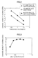
- Figure 2 shows the measurement-based relationship between channel mobility and threshold voltage in a MIS field-effect transistor with a gate electrode using P-type polycrystalline silicon, N-type polycrystalline silicon, and aluminum.
- channel mobility is higher with a gate electrode that uses N-type polycrystalline silicon or aluminum is used, compared to a gate electrode using P-type polycrystalline silicon. This might be attributable to the fact that, depending on the gate electrode polarity, a different amount of ion implantation is required to achieve the same threshold voltage.
- Implantation of N-type impurity into the buried channel region 2 results in the center of the channel being formed at a deep location, away from the interface between the gate insulation layer and the P-type silicon carbide substrate 1.
- Figure 3 is a measured result showing the L bc /X j dependency of the channel mobility, when the junction depth X j of the source/drain diffusion layer is 0.5 ⁇ m.
- the vertical axis shows the normalized channel mobility of a sample having no buried channel region. The evaluation was performed using an L bc /X j of 0.2 or above; it was confirmed that there was an effect even at 0.2. Therefore, the lower limit on the horizontal axis was set at 0.2. At over 1 on the horizontal axis, channel mobility increases, but the threshold voltage goes negative, resulting in a normally on state that makes the device difficult to use. Therefore, the horizontal axis is limited to 0.2 to 1.0. A range of 0.4 to 1.0 is particularly effective.
- Figure 4 shows the measured relationship between the impurity concentration of the P-type polycrystalline silicon gate and the threshold voltage.
- a higher concentration increases the difference of work function between gate and semiconductor, increasing the threshold voltage.
- a lower concentration decreases the threshold voltage, which at 1 x 10 16 cm -3 becomes zero. Therefore the lower limit for the impurity concentration is set at 1 x 10 16 cm -3 and the upper limit is set at 1 x 10 21 cm -3 .
- Figure 5 shows the measured relationship between channel mobility (using the value at an impurity concentration of zero as the standard value) and the impurity concentration of the buried channel region 2.
- the lower limit of the evaluation impurity concentration was 5 x 10 15 cm -3 . Since an adequate effect was achieved with that value, the lower limit was set at 5 x 10 16 cm -3 . With a concentration of 1 x 10 18 cm -3 or over, the threshold voltage goes negative, making the device hard to use, so the upper limit was set at 1 x 10 18 cm -3 .
- the gate voltage that gives rise to punch-through is the same as when there is no P + region, meaning there is no effect.
- a concentration of at least 1 x 10 17 cm -3 increases the gate voltage at which punch-through occurs, so the lower limit was set at 1 x 10 17 cm -3 .
- the impurity concentration is 1 x 10 19 cm -3 or higher, the impurity diffuses during activation annealing, offsetting the N-type impurity in the channel region above, making it impossible for the buried channel region to function as required. Therefore, the upper limit was set at 1 x 10 19 cm -3 .
- the resistivity of polycrystalline silicon given a high boron concentration is in the order of several m ⁇ cm, but the resistivity of the refractory metal silicides MoSi 2 , WSi 2 and TiSi 2 are 60 ⁇ cm, 50 ⁇ cm and 15 ⁇ cm, respectively. So, the resistivity of a gate electrode that is a composite of polycrystalline silicon and silicide is lower compared to polycrystalline silicon in which impurity has been implanted. This makes it possible to reduce the resistance of wiring, using long, thin gate electrodes or the gate electrode formation layer. By using the wiring resistance to reduce the time constant, the operating speed of the device can be improved.
- a P-type silicon carbide substrate 1 (impurity concentration: 5 x 10 15 cm -3 ) shown in Figure 1(a) was used.
- RIE reactive ion etching
- phosphorus ion implantation was used to form a buried channel region 2 at a junction depth L bc of 0.3, using multiple implantations at 40 keV to 250 keV to provide a total dose for a concentration of 7 x 10 15 cm -2 .
- an LTO layer was formed over the whole surface and photolithography was used to leave the gate electrode portion resist, with hydrofluoric acid being used to etch the LTO layer.
- ion implantation of phosphorus at 500°C was used to form a low-impurity-concentration region 11 between the buried channel region 2 and the source 5 and drain 6 having an impurity concentration of 5 x 10 16 cm -3 to 5 x 10 20 cm -3 .
- an LTO layer was formed over the whole surface and photolithography used to form a photoresist to define the source and drain regions, and hydrofluoric acid was used to etch the LTO and expose the ion implantation source and drain regions.
- the source 5 and drain 6 were then formed using multiple ion implantations at 500°C to form a phosphorus concentration of 5 x 10 19 cm -3 . This was followed by activation annealing for 30 minutes at 1500°Cin an argon atmosphere, and oxidation at 1200°C for 150 minutes, forming the gate insulation layer 7 approximately 50 nm thick shown in Figure 1 (c).
- the P-type gate electrode was then formed by using the CVD method to form polycrystalline silicon, using spin-coating to form a boron-containing oxide film on the polycrystalline silicon, followed by 30 minutes of heat treatment at 900°C to diffuse boron from the boron-containing oxide film to the polycrystalline silicon.
- the P-type polycrystalline silicon and the gate insulation layer were then etched to form the gate electrode.
- LTO was deposited over the whole surface of the oxide layer and the oxide film over the source 5 and drain 6 was etched to form contact holes.
- the electron-beam evaporation method was then used to form a nickel over-layer and wet etching was used to form metal wires 10.
- the samples were then heat-treated for 5 minutes at 1000°C in an argon atmosphere, thereby completing the fabrication of MIS field-effect transistors.
- the transistors were subjected to an electrical stress for a set time and and the degree by which the threshold voltage changed was measured to evaluate hot-carrier endurance. A smaller change in threshold voltage indicated good hot-carrier endurance.
- the threshold voltage was defined as the gate voltage that square root of drain current intersects the gate voltage axis, where the drain current was measured as a function of the gate voltage which was swept from 0V to 30V with a drain voltage of 0.1V.
- the electrical stress comprised applying 5 volts to the drain and 2.5 volts to the gate, for five minutes. Ion implantation of phosphorus was used to form an impurity concentration of 5 x 10 16 cm -3 to 5 x 10 19 cm -3 between the buried channel region 2 and the source/drain regions. A low impurity concentration in this region will result in a smaller field in the vicinity of the drain, making it possible to prevent electrons that pass through the region from entering a high-energy state, thereby improving hot-carrier endurance by decreasing the number of electrons that is injected into the gate insulation layer from the substrate. However, if the impurity concentration of this region is too low, the resistance of the region will become too high, reducing the driving force of the transistor.
- the lower limit is set at 5 x 10 16 cm -3 . If the concentration is too high, the field in the vicinity of the drain will not be alleviated, making it impossible to attain sufficient hot-carrier endurance. From measurements, it was found that with a concentration of 5 x 10 19 cm -3 or higher, the change in threshold voltage exceeded 10%, an amount that makes the device unusable. Therefore, the upper limit was set at 5 x 10 19 cm -3 .
- P-type silicon carbide substrates 1 with hexagonal silicon carbide crystalline (0001) and (11-20) surfaces were subjected to RCA cleaning, and reactive ion etching (RIE) was used to form photolithography alignment marks on the substrates.
- RIE reactive ion etching
- Phosphorus ion implantation was then used to form a buried channel region 2 at a junction depth L bc of 0.3, using multiple implantations at 40 keV to 250 keV to provide a total dose for a concentration of 7 x 10 15 cm -2 .
- an ion implantation mask 4 for the source and drain regions shown in Figure 1 (b) thermal oxidation or chemical vapor deposition (CVD) was used to form a SiO 2 layer.
- a low-temperature oxide (LTO) layer was used for the implantation mask.
- the LTO layer was formed by reacting silane and oxygen at 400°C to 800°C to form silicon dioxide, which was deposited on the substrate 1.
- a photoresist was then used to define the source and drain regions, and hydrofluoric acid was used to etch the LTO to form an opening to the source/drain regions that are to be subjected to the ion implantation.
- the source 5 and drain 6 of Figure 1(b) were then formed using phosphorus ion implantation steps effected at 500°C to achieve an impurity concentration of 5 x 10 19 cm -3 . This was followed by activation annealing for 30 minutes at 1500°C in an argon atmosphere. This was followed by oxidation at 1200°C for 150 minutes, forming the approximately 50 nm gate insulation layer 7, as shown in Figure 1 (c). After annealing for 30 minutes in an argon atmosphere, the samples were cooled in argon to room temperature.
- the P-type gate electrode 8 was then formed using the CVD method to form polycrystalline silicon and using spin-coating to form a boron-containing oxide film on the polycrystalline silicon, followed by 30 minutes of heat treatment at 900°C to diffuse boron from the boron-containing oxide film to the polycrystalline silicon.
- the P-type polycrystalline silicon and the gate insulation layer were then etched to form the gate electrode.
- the oxide film over the source and drain regions was then etched to form contact holes.
- the electron-beam evaporation method was then used to form a nickel over-layer and wet etching was used to form metal wires 10. To form a good ohmic contact, the samples were then heat-treated for 5 minutes at 1000°C in an argon atmosphere, thereby completing the fabrication of the MIS field-effect transistors.
- the MIS field-effect transistors thus fabricated on a (0001) surface had a channel mobility of 70 cm 2 /Vs, while MIS field-effect transistors fabricated on an (11-20) surface had a channel mobility of 100 cm 2 /Vs.
- the channel mobility was improved by fabricating MIS field-effect transistors on a (11-20) surface.
- Figure 6 shows an example of a type of MOSFET structure referred to as a lateral resurf or lateral DMOS type structure.
- Ion implantation can also be used to form a lateral resurf or lateral DMOS type MOSFET with a P-well, as shown in Figure 7.
- the P-well is formed as follows. The surface of a P-type epitaxially grown SiC substrate layer is subjected to multiple boron ion implantation steps at 30 to 160 keV, using dosages ranging from 1.5 to 36 x 10 13 cm -2 , which is followed by 30 minutes of annealing at 1600°C, thereby forming the P-well.
- the P-well can also be formed using aluminum. The remaining process steps are the same as those described with respect to the preceding examples.
- the above-described transistor structure can also be applied to the DMOS type MOSFET shown in Figure 8, by making the slight modifications described below.
- the modifications relate to the substrate and well formation, and require the following additional processes.
- a SiC layer is epitaxially grown on an N + substrate, over the drain, and another N + layer is formed on the first N + layer, and the surface thereof is subjected to multiple boron ion implantation steps at 30 to 160 keV, using dosages ranging from 1.5 to 36 x 10 13 cm -2 , which is followed by 30 minutes of annealing at 1600°C, thereby forming the P-well.
- the P-well can also be formed using aluminum.
- the remaining process steps are the same as those described with respect to the preceding examples.
- the material of the semiconductor region is silicon carbide
- the invention is not limited thereto, with the same effect being obtained with a substrate having a semiconductor region of diamond, silicon, gallium nitride or other such semiconductor material.
- Using a P-type gate electrode makes it possible to use a relatively high N - concentration without the device assuming a normally on state, thereby making it possible to increase channel mobility.
- Channel mobility is also improved when optimizing the ratio between the source/drain junction depth L bc and the junction depth of the buried channel region junction.
- the channel mobility can also be improved by the optimization of the P-type polycrystalline silicon concentration, and the concentration of the buried channel region.
- Device driving power can be raised when reducing the gate resistance by forming a refractory metal silicide layer over the P-type polycrystalline silicon gate electrode.
- the operating speed of the SiC semiconductor device can be increased using tungsten, molybdenum or titanium silicide layers.
- Hot-carrier endurance can be improved by the provision, between the buried channel formation region and the source and drain regions, a region having an impurity concentration that is not lower than the maximum impurity concentration of the impurity diffusion layer region used to form the buried channel region, and not higher than the impurity concentration of the source and drain regions.
- Punch-through endurance is improved by providing the P-type silicon carbide substrate 1 with a concentrated impurity region that is located beneath the buried channel region, and by optimizing the concentration of the region.
- Channel mobility is also improved by fabricating the device on the (11-20) surface of a hexagonal or rhombohedral or a (110) surface of a cubic system silicon carbide crystal.
- a high-power transistor can be readily realized by forming the device as a transistor having a lateral resurf or lateral DMOS type MOSFET structure. Also, the device can be readily fabricated as a normally off transistor by using aluminum or an aluminum alloy for the gate electrode.
Landscapes
- Insulated Gate Type Field-Effect Transistor (AREA)
Abstract
Description
Claims (14)
- A SiC semiconductor device comprising: a semiconductor substrate having a region formed of P-type silicon carbide (1), a gate insulation layer (7) formed on the P-type region, a P-type gate electrode (8) formed on the gate insulation layer, an N-type impurity region (2) having a sufficient impurity concentration to form a buried channel region (3) in a semiconductor layer below the gate insulation layer, and source and drain regions (5, 6) comprised of N-type impurity regions formed adjacent to the gate insulation layer and gate electrode.
- A device according to claim 1, wherein the ratio (Lbc/Xj) is not less than 0.2 and not more than 1.0, where the Lbc is the depth from the interface between the gate insulation layer and the silicon carbide to the buried channel region, and the Xjis the depth from the interface between the gate insulation layer and the silicon carbide to the source and drain region junction.
- A device according to claim 1 or 2, wherein the gate electrode is comprised of polycrystalline silicon in which boron or aluminum is diffused at a concentration within a range of from 1 x 1016cm-3 to 1 x 1021cm-3.
- A device according to claim 1 or 2, wherein the buried channel region contains a diffusion of nitrogen, phosphorus, or arsenic at a maximum concentration that is from 5 x 1015cm-3 to 1 x 1018cm-3.
- A device according to claim 1, 2, 3 or 4, wherein the gate electrode includes a silicide layer of a refractory metal.
- A device according to claim 5, wherein the refractory metal of the silicide layer is tungsten, molybdenum or titanium.
- A device according to claim 1, 2, 3, 4, 5 or 6 wherein between the buried channel formation region and the source and drain regions there is a region having an impurity concentration that is not lower than a maximum impurity concentration of the impurity diffusion layer region used to form the buried channel region, and not higher than an impurity concentration of the source or drain regions.
- A device according to claim 7, wherein between the buried channel formation region and the source and drain regions there is a diffusion layer of nitrogen, phosphorus, or arsenic at a maximum concentration that is from 5 x 1016cm-3 to 1 x 1019cm-3.
- A device according to claim 1, 2, 3, 4, 5, 6, 7 or 8, wherein there is a P-type impurity diffusion region having an impurity concentration that is higher than an impurity concentration of the semiconductor substrate, said P-type impurity diffusion region being located adjacently beneath the buried channel formation region.
- A device according to claim 9, wherein there is a high-concentration P-type impurity diffusion region located adjacently beneath the buried channel formation region that includes an aluminum or boron diffusion layer having a maximum impurity cuncentration of 1 x 1017cm-3 to 1 x 1019cm-3.
- A device according to claim 1, 2, 3, 4, 5, 6, 7, 8, 9 or 10, wherein the device is formed on a (11-20) surface of a hexagonal or rhombohedral or a (110) surface of a cubic system silicon carbide crystal.
- A device according to any of claims 1 to 11 having a lateral resurf or lateral DMOS type MOSFET structure.
- A device according to any of claims 1 to 11 having a DMOS type MOSFET structure.
- A device according to any of claims 1 to 13, wherein the gate electrode is formed of aluminum or an alloy that contains aluminum.
Applications Claiming Priority (2)
| Application Number | Priority Date | Filing Date | Title |
|---|---|---|---|
| JP2000346455A JP3881840B2 (en) | 2000-11-14 | 2000-11-14 | Semiconductor device |
| JP2000346455 | 2000-11-14 |
Publications (2)
| Publication Number | Publication Date |
|---|---|
| EP1205981A2 true EP1205981A2 (en) | 2002-05-15 |
| EP1205981A3 EP1205981A3 (en) | 2005-01-12 |
Family
ID=18820322
Family Applications (1)
| Application Number | Title | Priority Date | Filing Date |
|---|---|---|---|
| EP01309581A Withdrawn EP1205981A3 (en) | 2000-11-14 | 2001-11-13 | SiC MISFET |
Country Status (4)
| Country | Link |
|---|---|
| US (1) | US6759684B2 (en) |
| EP (1) | EP1205981A3 (en) |
| JP (1) | JP3881840B2 (en) |
| KR (1) | KR100860891B1 (en) |
Cited By (1)
| Publication number | Priority date | Publication date | Assignee | Title |
|---|---|---|---|---|
| EP3076431A4 (en) * | 2013-11-28 | 2017-08-09 | Rohm Co., Ltd. | Semiconductor device |
Families Citing this family (51)
| Publication number | Priority date | Publication date | Assignee | Title |
|---|---|---|---|---|
| US6956238B2 (en) * | 2000-10-03 | 2005-10-18 | Cree, Inc. | Silicon carbide power metal-oxide semiconductor field effect transistors having a shorting channel and methods of fabricating silicon carbide metal-oxide semiconductor field effect transistors having a shorting channel |
| JP4843854B2 (en) * | 2001-03-05 | 2011-12-21 | 住友電気工業株式会社 | MOS device |
| US7338869B2 (en) * | 2002-06-28 | 2008-03-04 | National Institute Of Advanced Industrial Science And Technology | Semiconductor device and its manufacturing method |
| WO2004036655A1 (en) * | 2002-10-18 | 2004-04-29 | National Institute Of Advanced Industrial Science And Technology | Silicon carbide semiconductor device and its manufacturing method |
| JP4063050B2 (en) * | 2002-10-31 | 2008-03-19 | 豊田合成株式会社 | Electrode of p-type group III nitride compound semiconductor and method for producing the same |
| KR20050084685A (en) * | 2002-11-25 | 2005-08-26 | 도꾸리쯔교세이호진 상교기쥬쯔 소고겡뀨죠 | Semiconductor device and power converter, driving inverter, general-purpose inverter and high-power high-frequency communication device using same |
| US7221010B2 (en) * | 2002-12-20 | 2007-05-22 | Cree, Inc. | Vertical JFET limited silicon carbide power metal-oxide semiconductor field effect transistors |
| US7074643B2 (en) * | 2003-04-24 | 2006-07-11 | Cree, Inc. | Silicon carbide power devices with self-aligned source and well regions and methods of fabricating same |
| US6979863B2 (en) * | 2003-04-24 | 2005-12-27 | Cree, Inc. | Silicon carbide MOSFETs with integrated antiparallel junction barrier Schottky free wheeling diodes and methods of fabricating the same |
| US7410846B2 (en) * | 2003-09-09 | 2008-08-12 | International Business Machines Corporation | Method for reduced N+ diffusion in strained Si on SiGe substrate |
| US7275357B2 (en) * | 2004-03-30 | 2007-10-02 | Cnh America Llc | Cotton module program control using yield monitor signal |
| US7118970B2 (en) | 2004-06-22 | 2006-10-10 | Cree, Inc. | Methods of fabricating silicon carbide devices with hybrid well regions |
| US7179696B2 (en) * | 2004-09-17 | 2007-02-20 | Texas Instruments Incorporated | Phosphorus activated NMOS using SiC process |
| US7476594B2 (en) * | 2005-03-30 | 2009-01-13 | Cree, Inc. | Methods of fabricating silicon nitride regions in silicon carbide and resulting structures |
| US7615801B2 (en) * | 2005-05-18 | 2009-11-10 | Cree, Inc. | High voltage silicon carbide devices having bi-directional blocking capabilities |
| US7414268B2 (en) | 2005-05-18 | 2008-08-19 | Cree, Inc. | High voltage silicon carbide MOS-bipolar devices having bi-directional blocking capabilities |
| US20060261346A1 (en) * | 2005-05-18 | 2006-11-23 | Sei-Hyung Ryu | High voltage silicon carbide devices having bi-directional blocking capabilities and methods of fabricating the same |
| US7391057B2 (en) * | 2005-05-18 | 2008-06-24 | Cree, Inc. | High voltage silicon carbide devices having bi-directional blocking capabilities |
| US7528040B2 (en) * | 2005-05-24 | 2009-05-05 | Cree, Inc. | Methods of fabricating silicon carbide devices having smooth channels |
| US7728402B2 (en) * | 2006-08-01 | 2010-06-01 | Cree, Inc. | Semiconductor devices including schottky diodes with controlled breakdown |
| US8432012B2 (en) | 2006-08-01 | 2013-04-30 | Cree, Inc. | Semiconductor devices including schottky diodes having overlapping doped regions and methods of fabricating same |
| EP2631951B1 (en) * | 2006-08-17 | 2017-10-11 | Cree, Inc. | High power insulated gate bipolar transistors |
| US8835987B2 (en) | 2007-02-27 | 2014-09-16 | Cree, Inc. | Insulated gate bipolar transistors including current suppressing layers |
| KR100817093B1 (en) * | 2007-03-16 | 2008-03-26 | 삼성전자주식회사 | Semiconductor Device Including Island Region |
| JP4793293B2 (en) | 2007-03-16 | 2011-10-12 | 日産自動車株式会社 | Silicon carbide semiconductor device and manufacturing method thereof |
| JP2009212366A (en) * | 2008-03-05 | 2009-09-17 | Oki Semiconductor Co Ltd | Method of manufacturing semiconductor device |
| US8232558B2 (en) | 2008-05-21 | 2012-07-31 | Cree, Inc. | Junction barrier Schottky diodes with current surge capability |
| US8188538B2 (en) | 2008-12-25 | 2012-05-29 | Rohm Co., Ltd. | Semiconductor device and method of manufacturing semiconductor device |
| US8288220B2 (en) * | 2009-03-27 | 2012-10-16 | Cree, Inc. | Methods of forming semiconductor devices including epitaxial layers and related structures |
| US8294507B2 (en) | 2009-05-08 | 2012-10-23 | Cree, Inc. | Wide bandgap bipolar turn-off thyristor having non-negative temperature coefficient and related control circuits |
| US8193848B2 (en) | 2009-06-02 | 2012-06-05 | Cree, Inc. | Power switching devices having controllable surge current capabilities |
| US8629509B2 (en) * | 2009-06-02 | 2014-01-14 | Cree, Inc. | High voltage insulated gate bipolar transistors with minority carrier diverter |
| US8541787B2 (en) * | 2009-07-15 | 2013-09-24 | Cree, Inc. | High breakdown voltage wide band-gap MOS-gated bipolar junction transistors with avalanche capability |
| US8354690B2 (en) | 2009-08-31 | 2013-01-15 | Cree, Inc. | Solid-state pinch off thyristor circuits |
| JP5316428B2 (en) * | 2010-01-12 | 2013-10-16 | 三菱電機株式会社 | Silicon carbide semiconductor device and manufacturing method thereof |
| US9117739B2 (en) | 2010-03-08 | 2015-08-25 | Cree, Inc. | Semiconductor devices with heterojunction barrier regions and methods of fabricating same |
| US8415671B2 (en) | 2010-04-16 | 2013-04-09 | Cree, Inc. | Wide band-gap MOSFETs having a heterojunction under gate trenches thereof and related methods of forming such devices |
| US9142662B2 (en) | 2011-05-06 | 2015-09-22 | Cree, Inc. | Field effect transistor devices with low source resistance |
| US9029945B2 (en) | 2011-05-06 | 2015-05-12 | Cree, Inc. | Field effect transistor devices with low source resistance |
| WO2013036370A1 (en) | 2011-09-11 | 2013-03-14 | Cree, Inc. | High current density power module comprising transistors with improved layout |
| US9373617B2 (en) | 2011-09-11 | 2016-06-21 | Cree, Inc. | High current, low switching loss SiC power module |
| US8680587B2 (en) | 2011-09-11 | 2014-03-25 | Cree, Inc. | Schottky diode |
| US9640617B2 (en) | 2011-09-11 | 2017-05-02 | Cree, Inc. | High performance power module |
| US8618582B2 (en) | 2011-09-11 | 2013-12-31 | Cree, Inc. | Edge termination structure employing recesses for edge termination elements |
| US8664665B2 (en) | 2011-09-11 | 2014-03-04 | Cree, Inc. | Schottky diode employing recesses for elements of junction barrier array |
| KR101386135B1 (en) * | 2012-11-29 | 2014-04-17 | 한국전기연구원 | Manufacturing method for decreasing interface states of sic/sio2 interface |
| JP5928429B2 (en) * | 2013-09-30 | 2016-06-01 | サンケン電気株式会社 | Semiconductor device and manufacturing method thereof |
| WO2016092960A1 (en) * | 2014-12-08 | 2016-06-16 | 富士電機株式会社 | Silicon carbide semiconductor device and process for producing same |
| CN107093548B (en) * | 2017-04-20 | 2019-09-03 | 泰科天润半导体科技(北京)有限公司 | Method for preparing SiC-based MOS device gate dielectric thin film |
| US10644018B2 (en) | 2018-04-12 | 2020-05-05 | Macronix International Co., Ltd. | 3D memory having plural lower select gates |
| CN115083920B (en) * | 2022-08-22 | 2022-11-15 | 泰科天润半导体科技(北京)有限公司 | Fabrication method of silicon carbide MOSFET with adjustable charge balance threshold voltage |
Family Cites Families (16)
| Publication number | Priority date | Publication date | Assignee | Title |
|---|---|---|---|---|
| US4017888A (en) * | 1975-12-31 | 1977-04-12 | International Business Machines Corporation | Non-volatile metal nitride oxide semiconductor device |
| US4714519A (en) * | 1987-03-30 | 1987-12-22 | Motorola, Inc. | Method for fabricating MOS transistors having gates with different work functions |
| JP3084301B2 (en) | 1991-04-23 | 2000-09-04 | ティーディーケイ株式会社 | Evaluation method of physical properties of hydrocarbon film using low energy electron spectroscopy |
| US5814869A (en) * | 1992-01-28 | 1998-09-29 | Thunderbird Technologies, Inc. | Short channel fermi-threshold field effect transistors |
| TW425637B (en) * | 1993-01-18 | 2001-03-11 | Semiconductor Energy Lab | Method of fabricating mis semiconductor device |
| JP2910573B2 (en) | 1993-09-10 | 1999-06-23 | 株式会社日立製作所 | Field effect transistor and method of manufacturing the same |
| US5736753A (en) * | 1994-09-12 | 1998-04-07 | Hitachi, Ltd. | Semiconductor device for improved power conversion having a hexagonal-system single-crystal silicon carbide |
| US5627385A (en) * | 1995-08-28 | 1997-05-06 | Motorola, Inc. | Lateral silicon carbide transistor |
| JPH11261061A (en) * | 1998-03-11 | 1999-09-24 | Denso Corp | Silicon carbide semiconductor device and method of manufacturing the same |
| DE19809554B4 (en) * | 1997-03-05 | 2008-04-03 | Denso Corp., Kariya | silicon carbide semiconductor device |
| US5952701A (en) * | 1997-08-18 | 1999-09-14 | National Semiconductor Corporation | Design and fabrication of semiconductor structure having complementary channel-junction insulated-gate field-effect transistors whose gate electrodes have work functions close to mid-gap semiconductor value |
| TW383909U (en) * | 1997-12-19 | 2000-03-01 | United Microelectronics Corp | Memory cell for flash erasable read only memory |
| JPH11251592A (en) * | 1998-01-05 | 1999-09-17 | Denso Corp | Silicon carbide semiconductor device |
| JP3216804B2 (en) * | 1998-01-06 | 2001-10-09 | 富士電機株式会社 | Manufacturing method of silicon carbide vertical FET and silicon carbide vertical FET |
| JP2000040791A (en) * | 1998-07-22 | 2000-02-08 | Toshiba Corp | Semiconductor device and manufacture thereof |
| JP3428459B2 (en) * | 1998-09-01 | 2003-07-22 | 富士電機株式会社 | Silicon carbide n-channel MOS semiconductor device and method of manufacturing the same |
-
2000
- 2000-11-14 JP JP2000346455A patent/JP3881840B2/en not_active Expired - Lifetime
-
2001
- 2001-11-13 EP EP01309581A patent/EP1205981A3/en not_active Withdrawn
- 2001-11-14 KR KR1020010070801A patent/KR100860891B1/en not_active Expired - Fee Related
- 2001-11-14 US US09/987,271 patent/US6759684B2/en not_active Expired - Lifetime
Cited By (8)
| Publication number | Priority date | Publication date | Assignee | Title |
|---|---|---|---|---|
| EP3076431A4 (en) * | 2013-11-28 | 2017-08-09 | Rohm Co., Ltd. | Semiconductor device |
| US9917102B2 (en) | 2013-11-28 | 2018-03-13 | Rohm Co., Ltd. | Semiconductor device |
| US10438971B2 (en) | 2013-11-28 | 2019-10-08 | Rohm Co., Ltd. | Semiconductor device |
| US10886300B2 (en) | 2013-11-28 | 2021-01-05 | Rohm Co., Ltd. | Semiconductor device |
| US11367738B2 (en) | 2013-11-28 | 2022-06-21 | Rohm Co., Ltd. | Semiconductor device |
| EP3644363B1 (en) * | 2013-11-28 | 2022-11-09 | Rohm Co., Ltd. | Semiconductor device |
| EP4141953A1 (en) * | 2013-11-28 | 2023-03-01 | Rohm Co., Ltd. | Semiconductor device |
| US11908868B2 (en) | 2013-11-28 | 2024-02-20 | Rohm Co., Ltd. | Semiconductor device |
Also Published As
| Publication number | Publication date |
|---|---|
| KR100860891B1 (en) | 2008-09-29 |
| US20020047125A1 (en) | 2002-04-25 |
| JP2002151680A (en) | 2002-05-24 |
| EP1205981A3 (en) | 2005-01-12 |
| US6759684B2 (en) | 2004-07-06 |
| JP3881840B2 (en) | 2007-02-14 |
| KR20020037447A (en) | 2002-05-21 |
Similar Documents
| Publication | Publication Date | Title |
|---|---|---|
| US6759684B2 (en) | SiC semiconductor device | |
| US6812102B2 (en) | Semiconductor device manufacturing method | |
| US9559188B2 (en) | Trench gate type semiconductor device and method of producing the same | |
| EP0671056B1 (en) | Power mosfet in silicon carbide | |
| US9490364B2 (en) | Semiconductor transistor having a stressed channel | |
| EP1450394B1 (en) | Semiconductor device and method for manufacturing same | |
| US6238980B1 (en) | Method for manufacturing silicon carbide MOS semiconductor device including utilizing difference in mask edges in implanting | |
| TWI382537B (en) | High mobility trench metal oxide semiconductor field effect transistor | |
| CN105051868B (en) | Semiconductor device | |
| US7508032B2 (en) | High voltage device with low on-resistance | |
| JP2003318396A (en) | Vertical MOSFET and manufacturing method thereof | |
| US20200176596A1 (en) | Metal oxide semiconductor (mos) controlled devices and methods of making the same | |
| JP4188637B2 (en) | Semiconductor device | |
| JP2013219161A (en) | Semiconductor device and semiconductor device manufacturing method | |
| TWI502741B (en) | Semiconductor device with high performance channel | |
| US20020195655A1 (en) | Symmetric trench MOSFET device and method of making same | |
| JP4842527B2 (en) | Manufacturing method of semiconductor device | |
| CN110828456A (en) | Si layer for oxygen insertion to reduce substrate dopant outdiffusion in power devices | |
| JP2010129628A (en) | Method of manufacturing silicon carbide semiconductor device | |
| WO1997049124A1 (en) | A method for producing a channel region layer in a voltage controlled semiconductor device | |
| JP3924085B2 (en) | Manufacturing method of vertical MOSFET | |
| EP0958601A1 (en) | A method for producing a channel region layer in a voltage controlled semiconductor device |
Legal Events
| Date | Code | Title | Description |
|---|---|---|---|
| PUAI | Public reference made under article 153(3) epc to a published international application that has entered the european phase |
Free format text: ORIGINAL CODE: 0009012 |
|
| AK | Designated contracting states |
Kind code of ref document: A2 Designated state(s): AT BE CH CY DE DK ES FI FR GB GR IE IT LI LU MC NL PT SE TR |
|
| AX | Request for extension of the european patent |
Free format text: AL;LT;LV;MK;RO;SI |
|
| RIN1 | Information on inventor provided before grant (corrected) |
Inventor name: ADACHI, KAZUHIRO, C/O NAT.INST. OF ADV. SCIENCE&T Inventor name: KOSUGI, RYOJI, C/O NAT.INST.OF AIST Inventor name: HARADA, SHINSUKE, C/O NAT.INST.OF AIST Inventor name: SENZAKI, JUNJI, C/O NAT.INST.OF AIST Inventor name: ARAI, KAZUO, C/O NAT.INST.OF AIST Inventor name: FUKUDA, KENJI, C/O NAT.INST.OF AIST |
|
| PUAL | Search report despatched |
Free format text: ORIGINAL CODE: 0009013 |
|
| AK | Designated contracting states |
Kind code of ref document: A3 Designated state(s): AT BE CH CY DE DK ES FI FR GB GR IE IT LI LU MC NL PT SE TR |
|
| AX | Request for extension of the european patent |
Extension state: AL LT LV MK RO SI |
|
| 17P | Request for examination filed |
Effective date: 20050422 |
|
| 17Q | First examination report despatched |
Effective date: 20050704 |
|
| AKX | Designation fees paid |
Designated state(s): DE |
|
| STAA | Information on the status of an ep patent application or granted ep patent |
Free format text: STATUS: THE APPLICATION IS DEEMED TO BE WITHDRAWN |
|
| 18D | Application deemed to be withdrawn |
Effective date: 20060117 |