EP1205405B1 - Information recording medium and access device - Google Patents
Information recording medium and access device Download PDFInfo
- Publication number
- EP1205405B1 EP1205405B1 EP00987756A EP00987756A EP1205405B1 EP 1205405 B1 EP1205405 B1 EP 1205405B1 EP 00987756 A EP00987756 A EP 00987756A EP 00987756 A EP00987756 A EP 00987756A EP 1205405 B1 EP1205405 B1 EP 1205405B1
- Authority
- EP
- European Patent Office
- Prior art keywords
- unit
- information
- access
- tag
- radio
- Prior art date
- Legal status (The legal status is an assumption and is not a legal conclusion. Google has not performed a legal analysis and makes no representation as to the accuracy of the status listed.)
- Expired - Lifetime
Links
Images


Classifications
-
- G—PHYSICS
- G07—CHECKING-DEVICES
- G07F—COIN-FREED OR LIKE APPARATUS
- G07F7/00—Mechanisms actuated by objects other than coins to free or to actuate vending, hiring, coin or paper currency dispensing or refunding apparatus
- G07F7/08—Mechanisms actuated by objects other than coins to free or to actuate vending, hiring, coin or paper currency dispensing or refunding apparatus by coded identity card or credit card or other personal identification means
- G07F7/10—Mechanisms actuated by objects other than coins to free or to actuate vending, hiring, coin or paper currency dispensing or refunding apparatus by coded identity card or credit card or other personal identification means together with a coded signal, e.g. in the form of personal identification information, like personal identification number [PIN] or biometric data
- G07F7/1008—Active credit-cards provided with means to personalise their use, e.g. with PIN-introduction/comparison system
-
- G—PHYSICS
- G06—COMPUTING; CALCULATING OR COUNTING
- G06F—ELECTRIC DIGITAL DATA PROCESSING
- G06F12/00—Accessing, addressing or allocating within memory systems or architectures
- G06F12/14—Protection against unauthorised use of memory or access to memory
- G06F12/1458—Protection against unauthorised use of memory or access to memory by checking the subject access rights
- G06F12/1466—Key-lock mechanism
-
- G—PHYSICS
- G06—COMPUTING; CALCULATING OR COUNTING
- G06F—ELECTRIC DIGITAL DATA PROCESSING
- G06F21/00—Security arrangements for protecting computers, components thereof, programs or data against unauthorised activity
- G06F21/70—Protecting specific internal or peripheral components, in which the protection of a component leads to protection of the entire computer
- G06F21/78—Protecting specific internal or peripheral components, in which the protection of a component leads to protection of the entire computer to assure secure storage of data
- G06F21/79—Protecting specific internal or peripheral components, in which the protection of a component leads to protection of the entire computer to assure secure storage of data in semiconductor storage media, e.g. directly-addressable memories
-
- G—PHYSICS
- G06—COMPUTING; CALCULATING OR COUNTING
- G06K—GRAPHICAL DATA READING; PRESENTATION OF DATA; RECORD CARRIERS; HANDLING RECORD CARRIERS
- G06K19/00—Record carriers for use with machines and with at least a part designed to carry digital markings
- G06K19/06—Record carriers for use with machines and with at least a part designed to carry digital markings characterised by the kind of the digital marking, e.g. shape, nature, code
- G06K19/067—Record carriers with conductive marks, printed circuits or semiconductor circuit elements, e.g. credit or identity cards also with resonating or responding marks without active components
- G06K19/07—Record carriers with conductive marks, printed circuits or semiconductor circuit elements, e.g. credit or identity cards also with resonating or responding marks without active components with integrated circuit chips
- G06K19/0723—Record carriers with conductive marks, printed circuits or semiconductor circuit elements, e.g. credit or identity cards also with resonating or responding marks without active components with integrated circuit chips the record carrier comprising an arrangement for non-contact communication, e.g. wireless communication circuits on transponder cards, non-contact smart cards or RFIDs
-
- G—PHYSICS
- G06—COMPUTING; CALCULATING OR COUNTING
- G06K—GRAPHICAL DATA READING; PRESENTATION OF DATA; RECORD CARRIERS; HANDLING RECORD CARRIERS
- G06K19/00—Record carriers for use with machines and with at least a part designed to carry digital markings
- G06K19/06—Record carriers for use with machines and with at least a part designed to carry digital markings characterised by the kind of the digital marking, e.g. shape, nature, code
- G06K19/067—Record carriers with conductive marks, printed circuits or semiconductor circuit elements, e.g. credit or identity cards also with resonating or responding marks without active components
- G06K19/07—Record carriers with conductive marks, printed circuits or semiconductor circuit elements, e.g. credit or identity cards also with resonating or responding marks without active components with integrated circuit chips
- G06K19/077—Constructional details, e.g. mounting of circuits in the carrier
- G06K19/07749—Constructional details, e.g. mounting of circuits in the carrier the record carrier being capable of non-contact communication, e.g. constructional details of the antenna of a non-contact smart card
- G06K19/07758—Constructional details, e.g. mounting of circuits in the carrier the record carrier being capable of non-contact communication, e.g. constructional details of the antenna of a non-contact smart card arrangements for adhering the record carrier to further objects or living beings, functioning as an identification tag
-
- G—PHYSICS
- G06—COMPUTING; CALCULATING OR COUNTING
- G06Q—INFORMATION AND COMMUNICATION TECHNOLOGY [ICT] SPECIALLY ADAPTED FOR ADMINISTRATIVE, COMMERCIAL, FINANCIAL, MANAGERIAL OR SUPERVISORY PURPOSES; SYSTEMS OR METHODS SPECIALLY ADAPTED FOR ADMINISTRATIVE, COMMERCIAL, FINANCIAL, MANAGERIAL OR SUPERVISORY PURPOSES, NOT OTHERWISE PROVIDED FOR
- G06Q10/00—Administration; Management
- G06Q10/08—Logistics, e.g. warehousing, loading or distribution; Inventory or stock management
-
- G—PHYSICS
- G06—COMPUTING; CALCULATING OR COUNTING
- G06Q—INFORMATION AND COMMUNICATION TECHNOLOGY [ICT] SPECIALLY ADAPTED FOR ADMINISTRATIVE, COMMERCIAL, FINANCIAL, MANAGERIAL OR SUPERVISORY PURPOSES; SYSTEMS OR METHODS SPECIALLY ADAPTED FOR ADMINISTRATIVE, COMMERCIAL, FINANCIAL, MANAGERIAL OR SUPERVISORY PURPOSES, NOT OTHERWISE PROVIDED FOR
- G06Q20/00—Payment architectures, schemes or protocols
- G06Q20/30—Payment architectures, schemes or protocols characterised by the use of specific devices or networks
- G06Q20/34—Payment architectures, schemes or protocols characterised by the use of specific devices or networks using cards, e.g. integrated circuit [IC] cards or magnetic cards
- G06Q20/341—Active cards, i.e. cards including their own processing means, e.g. including an IC or chip
-
- G—PHYSICS
- G06—COMPUTING; CALCULATING OR COUNTING
- G06Q—INFORMATION AND COMMUNICATION TECHNOLOGY [ICT] SPECIALLY ADAPTED FOR ADMINISTRATIVE, COMMERCIAL, FINANCIAL, MANAGERIAL OR SUPERVISORY PURPOSES; SYSTEMS OR METHODS SPECIALLY ADAPTED FOR ADMINISTRATIVE, COMMERCIAL, FINANCIAL, MANAGERIAL OR SUPERVISORY PURPOSES, NOT OTHERWISE PROVIDED FOR
- G06Q20/00—Payment architectures, schemes or protocols
- G06Q20/30—Payment architectures, schemes or protocols characterised by the use of specific devices or networks
- G06Q20/36—Payment architectures, schemes or protocols characterised by the use of specific devices or networks using electronic wallets or electronic money safes
- G06Q20/367—Payment architectures, schemes or protocols characterised by the use of specific devices or networks using electronic wallets or electronic money safes involving electronic purses or money safes
- G06Q20/3674—Payment architectures, schemes or protocols characterised by the use of specific devices or networks using electronic wallets or electronic money safes involving electronic purses or money safes involving authentication
-
- G—PHYSICS
- G06—COMPUTING; CALCULATING OR COUNTING
- G06Q—INFORMATION AND COMMUNICATION TECHNOLOGY [ICT] SPECIALLY ADAPTED FOR ADMINISTRATIVE, COMMERCIAL, FINANCIAL, MANAGERIAL OR SUPERVISORY PURPOSES; SYSTEMS OR METHODS SPECIALLY ADAPTED FOR ADMINISTRATIVE, COMMERCIAL, FINANCIAL, MANAGERIAL OR SUPERVISORY PURPOSES, NOT OTHERWISE PROVIDED FOR
- G06Q20/00—Payment architectures, schemes or protocols
- G06Q20/38—Payment protocols; Details thereof
- G06Q20/40—Authorisation, e.g. identification of payer or payee, verification of customer or shop credentials; Review and approval of payers, e.g. check credit lines or negative lists
- G06Q20/409—Device specific authentication in transaction processing
- G06Q20/4097—Device specific authentication in transaction processing using mutual authentication between devices and transaction partners
-
- G—PHYSICS
- G07—CHECKING-DEVICES
- G07C—TIME OR ATTENDANCE REGISTERS; REGISTERING OR INDICATING THE WORKING OF MACHINES; GENERATING RANDOM NUMBERS; VOTING OR LOTTERY APPARATUS; ARRANGEMENTS, SYSTEMS OR APPARATUS FOR CHECKING NOT PROVIDED FOR ELSEWHERE
- G07C3/00—Registering or indicating the condition or the working of machines or other apparatus, other than vehicles
-
- G—PHYSICS
- G07—CHECKING-DEVICES
- G07C—TIME OR ATTENDANCE REGISTERS; REGISTERING OR INDICATING THE WORKING OF MACHINES; GENERATING RANDOM NUMBERS; VOTING OR LOTTERY APPARATUS; ARRANGEMENTS, SYSTEMS OR APPARATUS FOR CHECKING NOT PROVIDED FOR ELSEWHERE
- G07C9/00—Individual registration on entry or exit
- G07C9/20—Individual registration on entry or exit involving the use of a pass
- G07C9/28—Individual registration on entry or exit involving the use of a pass the pass enabling tracking or indicating presence
-
- G—PHYSICS
- G07—CHECKING-DEVICES
- G07F—COIN-FREED OR LIKE APPARATUS
- G07F7/00—Mechanisms actuated by objects other than coins to free or to actuate vending, hiring, coin or paper currency dispensing or refunding apparatus
- G07F7/02—Mechanisms actuated by objects other than coins to free or to actuate vending, hiring, coin or paper currency dispensing or refunding apparatus by keys or other credit registering devices
-
- H—ELECTRICITY
- H04—ELECTRIC COMMUNICATION TECHNIQUE
- H04W—WIRELESS COMMUNICATION NETWORKS
- H04W12/00—Security arrangements; Authentication; Protecting privacy or anonymity
- H04W12/08—Access security
- H04W12/086—Access security using security domains
-
- G—PHYSICS
- G06—COMPUTING; CALCULATING OR COUNTING
- G06F—ELECTRIC DIGITAL DATA PROCESSING
- G06F2221/00—Indexing scheme relating to security arrangements for protecting computers, components thereof, programs or data against unauthorised activity
- G06F2221/21—Indexing scheme relating to G06F21/00 and subgroups addressing additional information or applications relating to security arrangements for protecting computers, components thereof, programs or data against unauthorised activity
- G06F2221/2103—Challenge-response
-
- G—PHYSICS
- G06—COMPUTING; CALCULATING OR COUNTING
- G06F—ELECTRIC DIGITAL DATA PROCESSING
- G06F2221/00—Indexing scheme relating to security arrangements for protecting computers, components thereof, programs or data against unauthorised activity
- G06F2221/21—Indexing scheme relating to G06F21/00 and subgroups addressing additional information or applications relating to security arrangements for protecting computers, components thereof, programs or data against unauthorised activity
- G06F2221/2129—Authenticate client device independently of the user
-
- G—PHYSICS
- G06—COMPUTING; CALCULATING OR COUNTING
- G06F—ELECTRIC DIGITAL DATA PROCESSING
- G06F2221/00—Indexing scheme relating to security arrangements for protecting computers, components thereof, programs or data against unauthorised activity
- G06F2221/21—Indexing scheme relating to G06F21/00 and subgroups addressing additional information or applications relating to security arrangements for protecting computers, components thereof, programs or data against unauthorised activity
- G06F2221/2141—Access rights, e.g. capability lists, access control lists, access tables, access matrices
-
- H—ELECTRICITY
- H04—ELECTRIC COMMUNICATION TECHNIQUE
- H04W—WIRELESS COMMUNICATION NETWORKS
- H04W12/00—Security arrangements; Authentication; Protecting privacy or anonymity
- H04W12/40—Security arrangements using identity modules
- H04W12/47—Security arrangements using identity modules using near field communication [NFC] or radio frequency identification [RFID] modules
Definitions
- the present invention relates to techniques for attaching a contactless IC tag to an item which passes through multiple stages such as a manufacture stage, and accessing the contactless IG tag to manage the item.
- the item include vehicles, foodstuffs, houses, cloths, miscellaneous goods, and electronic equipment such as home electrical appliances.
- Japanese Laid-Open Patent Application No. H10-222568 discloses the following system to reduce the cost of the entire life cycle. Identification information such as model and production numbers, material information, operation information, error information, and maintenance information are recorded for each product and component, at each stage such as manufacture, use, and maintenance. The recorded information is read and put to use for evaluating the product in each of the stages including manufacture, maintenance, collection, and resale.
- Japanese Laid-Open Patent Application No. H11-120308 discloses a historical information storing device which attaches historical information of a product to the product itself.
- information relating to a product can be attached to the product and passed through each stage of the life cycle together with the product.
- This allows the information relating to the product to be shared and freely used at any stage of the life cycle such as manufacture, maintenance, collection, and resale.
- secret information cannot be attached to the product. This is one of the main reasons why the technique of distributing the product and the information relating to the product together in the life cycle has not been so widely used.
- EP-A-0856818 discloses a portable data carrier which includes a secure processing and a co-located directory.
- a memory element is substantially separated by the secure processing element and disposed within the portable data carrier.
- a secure processor command stemming from an operator input is then used to access a portion of the directory that includes and address key.
- DE-A-19522050 relates to a contact chip card capable of being used for different issuers such as credit card, bank card, travel card, all in one card.
- issuers such as credit card, bank card, travel card, all in one card.
- a different page is assigned to each issuer, and each page is protected by its own page identifier.
- the page identifier (“keys") may be given to various issuers as desired such that certain memory areas may be made "public”.
- EP-A-0713188 relates to a documentation system which has supplied authorisation information recorded in a chip card memory, with secure transmission of documentation information between the authorisation point and the chip card.
- Cryptographic storage of the authorisation is in the chip card memory.
- EP-A-0923056 discloses an IC card containing storage units to store data and an access control unit to control an access to the data by an access subject.
- the present invention aims to provide an information recording medium and contactless IC tag is attached to an item which passes through multiple stages.
- the invention also aims to provide an access device that is capable of reading/writing information from/to the contactless IC tag in secrecy for each stage, an access system made up of contactless IC tag and the access device, and a life cycle management system made up of the contactless IC tag and the access devices provided for the multiple stages.
- the invention further aims to provide and input/output method used for the contactless IC tag, and an access method used for the access device.
- the present invention relates to an information storage medium as set forth in claim 1.
- the access device can access the storage area identified by the access identifier which is received by the information recording medium in secrecy. Accordingly, a single information recording medium can be used for a plurality of purposes.
- the access device can access the stage storage area identified by the stage identifier which is received by the contactless IC tag in secrecy. Accordingly, a single contactless IC tag can be used for multiple stage of a lift cycle from manufacture to disposal.
- the contactless IC tag authenticates the access device without the stage identifier being sent, so that there is no risk of the stage identifier being revealed.
- the contactless IC tag generates the authenticator randomly, so that there is no risk of the stage identifier being revealed from past communications.
- the contactless IC tag performs communication with the access device using the time-multiplexing channels which enables the access device to communicate with more than one contactless IC tag at the same time.
- the contactless IC tag selects the communication channel at random, which reduces the possibility of the same communication channel being selected by the two contactless IC tags.
- the contactless IC tag is not so noticeable from the outside. This keeps the appearance of the item from being ruined. Also, since the position of the contactless IC tag is known to be near the logotype, the contactless IC tag can be easily found in each stage of the life cycle.
- date and time information can be written together with the item information. Therefore, even when there is not enough free memory when writing new item information, it is possible to automatically delete the oldest item information, or send a list of item information to the access device so that the user of the access device can choose which item information should be deleted. As a result, the new item information can be written to the memory.
- the new item information can be written to the extension storage area which is provided beforehand.
- the use of the access device can request the secret information to be revealed through the use of the master identifier.
- An advantage of the invention is a person who has the rights to operate an access device of each stage, such as a patient, a doctor, a nurse, or an accountant, inputs a password which only he or she knows, into the access device. Once the authenticity of the person has been verified, the access device reads/writes information from/to a corresponding stage storage area of the contactless IC tag. In this way, the patient can obtain proper knowledge of his or her condition and medical treatment. Also, the doctor or the nurse can be kept from confusing the patient with another patient or committing malpractice. Moreover, the accountant can calculate medical expenses accurately.
- a further advantage is the distribution of fake brand-name products can be prevented. Also, the quality of brand-name products can be ensured. Further, the management and tracking of the distribution route of the brand-name products can be made by writing route information to the contactless IC tag.
- the access device can be access the information recording medium which has the storage area identified by the secretly received access identifier.
- a single information recording medium can be used for a plurality of purposes.
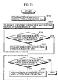
- Fig. 1 shows a life cycle 6 of a product from manufacture through to disposal/collection, namely, a complete lifetime of the product that passes through a series of stages including a manufacture stage 1, a distribution stage 2, a sale stage 3, a service stage 4 and a collection/recycle stage 5.
- FIG. 2 shows the state where a radio IC tag is attached to a front corner of a TV set and a logo mark is attached over the radio IC tag.
- FIG. 3 shows the state where a label to which a radio IC tag is attached is sewn on the back of the neck of cloths.
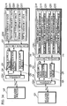
- FIG. 4 is a block diagram showing a construction of a life cycle management system 10.
- FIG. 5 is a block diagram showing a construction of a subsystem 2C
- FIG. 6 shows the state where a reader/writer 30a and management device 40a in a first group which belongs to a manufacture management subsystem 20a are equipped in a manufacturing factory.
- FIG. 7 shows the state where a reader/writer 30d and mobile-phone-equipped management device 40d in a third group which belongs to a distribution management subsystem 20b are mounted on a cargo truck.
- FIG. 6 shows the outward appearance of a mobile-phone-type reader/writer 30c in a second group which belongs to the distribution management subsystem 20b.
- FIG. 9 shows the outward appearance of a reader/writer 30b in the first group which belongs to a sale management subsystem 20c.
- FIG. 10 shows the outward appearance of a portable-terminal-type reader/writer 30e in a fourth group which belongs to a service management subsystem 20d.
- FIG. 11 is a block diagram showing a construction of a reader/writer 30.
- FIG. 12 shows a synchronous signal transmission period, an identification code acquisition period, and an access period.
- FIG. 13 shows instructions received by an instruction generating unit 104 and operands accompanying these instruction.
- FIG. 14 shows instructions extracted by an instruction decoding unit 110 and operands accompanying these instructions.
- FIG. 15 shows the outward appearance of a radio IC tag 80.
- FIG. 16 is a block diagram showing a construction of an IC chip unit 200 in the radio IC tag 80.
- FIG. 17 is a memory map showing a construction of a memory unit 216.
- FIG. 18 is a memory map showing a construction of the memory unit 216, where the contents of the memory unit 216 are shown for each stage area.
- FIG. 19 shows an example of a power supply circuit included in a power supply unit 203.
- FIG. 20 is a block diagram showing a construction of an authenticating unit 210.
- FIG. 21 is a block diagram showing constructions of a management device 40 and host computer 60.
- FIG. 22 shows an example of information stored in a database 61 in the host computer 60.
- FIG. 23 is a flowchart showing overall operations of the reader/writer 30 and radio IC tag 80.
- FIG. 24 is a diagram showing an operation of acquiring an identification code of the radio IC tag 80.
- FIG. 25 is a diagram showing an area access authentication operation and area access operation of the reader/writer 30 and radio IC tag 80.
- FIG. 26 shows the relations between applications of the radio IC tag 80, unit prices, and communication distances.
- FIG. 27 shows the outward appearance of a home washing machine equipped with a reader/writer similar to the reader/writer 30.
- FIG. 28 is an example memory map of a memory unit that includes an extension area.
- FIG. 29 is a diagram showing an area access authentication operation and an area access operation, when the reader/writer 30 performs reading/writing for only one radio IC tag.
- FIG. 30 shows a life cycle procedure of a life cycle management system according to a background example
- FIG. 31 is a block diagram showing a construction of a contactless IC tag and a reader/writer according to a background example of the invention.
- FIG. 32 is a block diagram showing a construction of a contactless IC tag and a reader/writer according to the second embodiment of the invention.
- FIG. 33 is a block diagram showing a construction of a contactless IC tag and a reader/writer according to the third embodiment of the invention.
- FIG. 34 is a block diagram showing a construction of a contactless IC tag and a reader/writer according to the fourth embodiment of the invention.
- life cycle management system 10 as the first embodiment of the invention.
- a manufacturer processes and assembles components to produce a product (item) in a manufacturing factory, and ships the product.
- a distributor transports the product to a seller.
- the seller sells the product to a consumer.
- the consumer uses the product.
- a service provider repairs/maintains the product used by the consumer.
- a collector/recycler dismantles and disposes the product after long years of use. Part of the dismantled product is put to use for recycling.
- the product passes through a manufacture stage 1, a distribution stage 2, a sale stage 3, a service stage 4, and a collection/recycle stage 5, before it ends its life, as shown in FIG. 1 .
- This lifetime of the product from manufacture through to disposal/collection is called a life cycle 6.
- the manufacturer attaches a radio IC tag (described later) to the product, in the manufacture process.
- a TV set manufacturer attaches a radio IC tag 80a to a front corner 81 of a TV set 82, and attaches a logo mark 83 on top of the radio IC tag 80a, as shown in FIG. 2 .
- an apparel manufacturer attaches a radio IC tag 80b to the reverse side of a label 93, and sews the label 93 to the back 91 of the neck of cloths 90, as shown in FIG. 3 .
- the radio IC tag has areas for storing information relating to the product.
- the manufacturer writes information about the manufacturing to the radio IC tag or refers to such information from the radio IC tag in the manufacture stage 1, to manage the manufacturing of the product.
- the distributor writes information about the transportation to the radio IC tag or refers to such information from the radio IC tag in the distribution stage 2, to manage the transportation of the product.
- the seller, the service provider, and the collector/recycler write information about their operations to the radio IC tag or refer to such information from the radio IC tag in the respective stages 3, 4, and 5, to manage the operations.
- the life cycle management system 10 includes a manufacture management subsystem 20a, a distribution management subsystem 20b, a sale management subsystem 20c, a service management subsystem 20d, a collection/recycle management subsystem 20e, and the Internet 30.
- the subsystems are connected to each other via the Internet 30.
- the manufacture management subsystem 20a, the distribution management subsystem 20b, the sale management subsystem 20c, the service management subsystem 20d, and the collection/recycle management subsystem 20e are each an information management system for managing the product by the manufacturer, the distributor, the seller, the service provider, and the collector/recycler, respectively.
- the manufacture management subsystem 20a, the distribution management subsystem 20b, the sale management subsystem 20c, the service management subsystem 20d, and the collection/recycle management subsystem 20e have a common construction. Accordingly, these subsystems are explained collectively as a subsystem 20 below.
- the subsystem 20 includes first to fourth groups, a radio IC tag 80 attached to a product, a host computer 60 having a database 61, and a LAN device 70.
- the first group is made up of a reader/writer 30a (30b) and a management device 40a (40b).
- the second group is made up of a mobile-phone-type reader/writer 30c, a base station 50, a receiver 51, and a connector 53.
- the third group is made up of a reader/writer 30d, a mobile-phone-equipped management device 40d, the base station 50, the receiver 51, and the connector 53.
- the fourth group is made up of a portable-terminal-type reader/writer 30e, an IC card 52, and a management device 40e.
- the reader/writer 30a (30b) is connected to the management device 40a (40b), which is connected to the LAN device 70.
- the mobile-phone-type reader/writer 30c communicates with the receiver 51 via the base station 50 and a public network.
- the receiver 51 is connected to the connector 53, which is connected to the LAN device 70.
- the reader/writer 30d is connected to the mobile-phone-equipped management device 40d, which communicates with the receiver 51 via the base station 50 and the public network.
- the receiver 51 is connected to the connector 53, which is connected to the LAN device 70.
- the IC card 52 is loaded to the portable-terminal-type reader/writer 30e or the management device 40e.
- the portable-terminal-type reader/writer 30e writes data to the IC card 52, or refers to data from the IC card 52.
- the management device 40e writes data to the IC card 52, or refers to data from the IC card 52.
- the management device 40e is connected to the LAN device 70.
- the host computer 60 is connected to the LAN device 70.
- the LAN device 70 is connected to the Internet 30.
- FIG. 6 shows the state where the reader/writer 30a and management device 40a in the first group which belongs to the manufacture management subsystem 20a are equipped in a manufacturing factory.
- TV sets to which radio IC tags are attached are packed in cardboard boxes which are being carried on a conveyor belt, in the manufacturing factory.
- the management device 40a is provided with a display unit, a body unit, and a keyboard unit, just like a personal computer.
- the reader/writer 30a is provided with a body unit having a cylindrical shape, and an antenna unit at the top end of the body unit. The reader/writer 30a is placed in the vicinity of the conveyor belt, so that radio waves emitted from the antenna unit will not be jammed between the antenna unit and the cardboard boxes passing near the reader/writer 30a.
- FIG. 7 shows the state where the reader/writer 30d and mobile-phone-equipped management device 40d in the third group which belongs to the distribution management subsystem 20b are mounted on a cargo truck.
- the mobile-phone-equipped management device 40d is equipped with a liquid crystal display unit, a body unit having a keyboard, and an antenna unit that transmits/receives radio waves to/from the base station 50.
- the mobile-phone-equipped management device 40d is placed in front of a front passenger seat of the cargo truck.
- the reader/writer 30d has an antenna unit, and is installed inside the cargo truck at the top of the carry-in entrance so that radio waves are transmitted in a downward direction.
- FIG. 8 shows the outward appearance of the mobile-phone-type reader/writer 30c in the second group which belongs to the distribution management subsystem 20b.
- the mobile-phone-type reader/writer 30c has a body unit shaped like a mobile phone.
- the mobile-phone-type reader/writer 30c also has an antenna unit on top of the body unit, which transmits/receives radio waves to/from the base station 50 and to/from the radio IC tag 80.
- the mobile-phone-type reader/writer 30c further has a plurality of operation buttons, a display unit, a microphone, and a speaker on the front of the body unit.
- FIG. 9 shows the outward appearance of the reader/writer 30b in the first group which belongs to the sale management subsystem 20c.
- the reader/writer 30b has a body unit shaped like a cylinder, and an antenna unit at the top of the body unit, which transmits/receives radio waves to/from the radio IC tag 80.
- the reader/writer 30b also has an operation button at one side of the body unit. This reader/writer 30b performs reading/writing of data simultaneously for a plurality of radio IC tags.
- FIG. 10 shows the outward appearance of the portable-terminal-type reader/writer 30e in the fourth group which belongs to the service management subsystem 20d.
- the portable-terminal-type reader/writer 30e has a body unit, an antenna unit for transmitting/receiving radio waves to/from the radio IC tag 80, and a printer unit. The antenna unit and the printer unit are positioned on top of the body unit.
- the portable-terminal-type reader/writer 30e also has a plurality of operation buttons and a display unit on the front of the body unit, and an IC card insertion slot at the bottom of the body unit. The IC card 52 is loaded to this IC card insertion slot.
- the management device 40e is provided with a display unit, a body unit, and a keyboard unit, like a personal computer.
- the management device 40e also has an IC card input/output unit, to which the IC card 52 is loaded.
- the reader/writers 30a, 30b, and 30d have the same construction. Also, the mobile-phone-type reader/writer 30c and the portable-terminal-type reader/writer 30e contain the same construction as the reader/writer 30a. Accordingly, these devices are collectively explained as a reader/writer 30 below.
- the reader/writer 30 is capable of simultaneously reading/writing information from/to fifty radio IC tags at the maximum. As shown in FIG. 11 , the reader/writer 30 includes an inputting/outputting unit 101, a. controlling unit 102, a temporary storing unit 103, an instruction generating unit 104, a clock generating unit 105, an identification code storing unit 106, a key storing unit 107, an encrypting unit 108, a hashing unit 109, an instruction decoding unit 110, a modulating/demodulating unit 111, and an antenna unit 112.
- the temporary storing unit 103 has fifty identification code areas for temporarily storing fifty identification codes that each identify a radio IC tag.
- the identification code storing unit 106 has fifty areas for storing fifty identification codes.
- the key storing unit 107 stores area key K1 for accessing a stage area (described later) of the radio IC tag 80 which the reader/writer 30 is permitted to access, and area key K6 for accessing a common area (described later) of the radio IC tag 80. These area keys are each 56 bits long.
- the key storing unit 107 may store one of area keys K2-K5 instead of area key K1.
- Area keys K2-K5 are each 56 bits long.
- the inputting/outputting unit 101 is connected to a management device 40 (described later), and receives a combination of an input/output instruction and input/output information from the management device 40.
- the input/output instruction is either an input instruction or an output instruction.
- the input instruction is to read data from memory of a radio IC tag, whereas the output instruction is to write data to the memory of the radio IC tag.
- the input/output instruction is an input instruction
- the input/output information includes a physical address of the memory of the radio IC tag and the number of bytes to be read.
- the input/output instruction is an output instruction
- the input/output information includes a physical address of the memory of the radio IC tag, the number of bytes to be written, and the contents of writing.
- the inputting/outputting unit 101 outputs the received input/output instruction and input/output information to the controlling unit 102.
- the inputting/outputting unit 101 also receives an access response instruction, access response information, and an identification code from the controlling unit 102, and outputs the received access response instruction, access response information, and identification code to the management device 40.
- the controlling unit 102 exercises control of charging radio wave transmission, synchronous signal transmission, identification code acquisition, and access, respectively in a charge radio wave transmission period, a synchronous signal transmission period, an identification code acquisition period, and an access period, as shown in FIG. 12 .
- horizontal axis represents time.
- the charging radio wave transmission period, the synchronous signal transmission period, the identification code acquisition period, and the access period are consecutive in this order on the time axis.
- the identification code acquisition period is made up of first and second acquisition periods.
- the first and second acquisition periods are each made up of an identification code transmission period, an identification code response period, and an identification code matching period, which each have a cycle of 500msec.
- One cycle is evenly divided into fifty blocks of 10msec. These 10msec blocks are called channels.
- the fifty channels which compose one cycle are channel 1, channel 2, channel 3, ... , and channel 50 beginning with the start of the cycle.
- the fifty channels are identified by these channel numbers.
- the controlling unit 102 receives the input/output instruction and the input/output information from the inputting /outputting unit 101.
- the controlling unit 102 then outputs a synchronous signal transmission instruction for transmitting a synchronous signal and an identification code acquisition instruction for acquiring an identification code of each radio IC tag, to the instructions generating unit 104 in this order.
- the Controlling unit 102 collects the identification code from each radio IC tag during the identification code acquisition period of 3 seconds, in the following manner. Once the identification code acquisition period has passed, the controlling unit 102 judges that the collection of the identification code of each radio IC tag has completed, and ends the identification code acquisition. As mentioned earlier, the identification code acquisition period is made up of the first and second acquisition periods, in each of which the controlling unit 102 exercises identification code transmission control, identification code response control, and identification code matching control. The reason why the acquisition is repeated twice in the first and second acquisition periods will be given later.
- the controlling unit 102 receives an identification code transmission instruction and an identification code from the instruction decoding unit 110, and a hash value from the hashing unit 109. On receiving the identification code transmission instruction, the controlling unit 102 writes the received identification code to an identification code area in the temporary storing unit 103 which is specified by the received hash value.
- the controlling unit 102 receives a reference clock from the clock generating unit 105, and generates a synchronous signal wave in which a synchronous signal made up of one pulse signal of 10msec is repeated. The controlling unit 102 then outputs the generated synchronous signal wave to the instruction generating unit 104 for 100msec.
- one cycle of the synchronous signal wave is 500msec.
- One cycle is evenly divided into fifty 10msec blocks which are each a channel.
- the controlling unit 102 selects a channel whose channel number matches the received hash value.
- the controlling unit 102 then outputs the received identification code and an identification code response instruction for transmitting the identification code, to the instruction generating unit 104 at the selected channel in the identification code response period.
- the controlling unit 102 Since the controlling unit 102 selects the channel by using the hash value as the channel number, the same channel may be selected for different radio IC tags. When this happens, the controlling unit 102 gives up collecting the identification codes of these radio IC tags in the first acquisition period, and instead collects the identification codes in the second acquisition period. There is only a little possibility that the same channel is selected for the different radio IC tags again in the second acquisition period.
- the controlling unit 102 waits for receiving an identification code matching instruction from the instruction decoding unit 110, at the selected channel in the identification code matching period. On receiving the identification code matching instruction at the selected channel, the controlling unit 102 judges that the identification code stored in the identification code area specified by the hash value in the temporary storing unit 103 is an identification code that properly identifies a radio IC tag. The controlling unit 102 then reads the identification code from the temporary storing unit 103, and writes it to the identification code storing unit 106.
- the controlling unit 102 performs an access request and an area access in the access period, for all radio IC tags identified by the identification codes stored in the identification code storing unit 106, in the following way.
- the controlling unit 102 reads an identification code from the identification code storing unit 106, and outputs an access request instruction for requesting access to a radio IC tag identified by the read identification code, and the read identification code, to the instruction generating unit 104.
- the controlling unit 102 then receives an authenticator transmission instruction and an identification code from the instruction decoding unit 110.
- the controlling unit 102 reads an area key (K1 or K6) stored in the key storing unit 107, and outputs the read area key (K1 or K6) to the encrypting unit 108.
- Which of area keys K1 and K6 is read is determined by the input/output information received from the inputting/outputting unit 101. Which is to say, when the physical address included in the input/output information shows an address in the stage area which the reader/writer 30 is permitted to access, area key K1 is read. When the physical address included in the input/output information shows an address in the common area, area key K6 is read.
- the controlling unit 102 then outputs the read identification code and an authentication response instruction to the instruction generating unit 104.
- the controlling unit 102 when receiving an access prohibition instruction, an identification code, and a reason code from the instruction decoding unit 110, the controlling unit 102 recognizes an operation error such as an error of area key K1 based on the reason code, and gives up accessing the radio IC tag identified by the identification code. The controlling unit 102 then generates an access response instruction and access response information that includes the reason code, and outputs the access response instruction, the access response information, and the identification code to the inputting/outputting unit 101. The controlling unit 102 generates an access instruction based on the input/output instruction, and generates access information based on the input/output information. The controlling unit 102 then outputs the read identification code, the access information, and the access instruction to the instruction generating unit 104.
- an operation error such as an error of area key K1 based on the reason code
- the controlling unit 102 then generates an access response instruction and access response information that includes the reason code, and outputs the access response instruction, the access response information, and the identification code to the inputting/outputting unit
- the controlling unit 102 When receiving an access response instruction, access response information, and an identification code from the instruction decoding unit 110, the controlling unit 102 outputs the access response instruction, the access response information, and the identification code to the inputting/outputting unit 101.
- each instruction is a code of 4 bits.
- the controlling unit 102 also controls the modulating/demodulating unit 111 to output a silence wave in periods during which radio waves are received from the radio IC tag. These periods are the identification code transmission period, the identification code matching period, and the access period, during which the reader/writer 30 receives data from the radio IC tag
- the instruction generating unit 104 receives the synchronous signal transmission instruction, the identification code acquisition instruction, the combination of the identification code and the identification code response instruction, the combination of the access request instruction and the identification code, the combination of the identification code and the authenticator response instruction, and the combination of the identification code, the access information, and the access instruction, from the controlling unit 102.
- the instruction generating unit 104 On receiving the synchronous signal transmission instruction from the controlling unit 102, the instruction generating unit 104 generates a pulse signal wave based on the synchronous signal transmission instruction, and outputs the generated pulse signal wave to the modulating/demodulating unit 111. Following this, the instruction generating unit 104 receives the synchronous signal wave from the controlling unit 102, generates a pulse signal wave of one second based on the received synchronous signal wave, and outputs the pulse signal wave to the modulating/demodulating unit 111.
- the instruction generating unit 104 When receiving the identification code acquisition instruction, the identification code response instruction, the access request instruction, the authenticator response instruction, or the access instruction from the controlling unit 102, the instruction generating unit 104 generates a pulse signal wave based on the received instruction, and outputs the generated pulse signal wave to the modulating/demodulating unit 111.
- the instruction generating unit 104 On receiving the identification code and the identification code response instruction from the controlling unit 102, the instruction generating unit 104 generates a pulse signal wave based on the identification code after outputting a pulse signal wave based on the identification code response instruction, and outputs the generated pulse signal wave to the modulating/demodulating unit 111.
- the instruction generating unit 104 On receiving the access request instruction and the identification code from the controlling unit 102, the instruction generating unit 104 generates a pulse signal wave based on the identification code after outputting a pulse signal wave based on the access request instruction, and outputs the generated pulse signal to the modulating/demodulating unit 111.
- the information generating unit 104 receives the identification code and the authenticator response instruction from the controlling unit 102, and receives encrypted random number R0' from the encrypting unit 108. After outputting a pulse signal wave based on the authenticator response instruction, the information generating unit 104 generates a pulse signal wave based on the identification code and encrypted random number R0', and outputs the generated pulse signal wave to the modulating/demodulating unit 111.
- the information generating unit 104 On receiving the identification code, the access information, and the access instruction from the controlling unit 102, the information generating unit 104 generates a pulse signal wave based on the identification code and the access information after outputting a pulse signal wave based on the access instruction, and outputs the generated pulse signal wave to the modulating/demodulating unit 111.
- the clock generating unit 105 repeatedly generates the reference clock which shows reference time, and outputs it to the controlling unit 102.
- the encrypting unit 108 has encryption algorithm E1.
- Encryption algorithm E1 is an encryption algorithm defined by DES (Data Encryption Standard) .
- An encryption key of encryption algorithm E1 is 56 bits long, and a plaintext inputted to encryption algorithm E1 and ciphertext generated by encryption algorithm E1 are both 64 bits long.
- the encrypting unit 108 receives the area key (K1 or K6) from the controlling unit 102, and receives random number R0 from the instruction decoding unit 110.
- the encrypting unit 108 encrypts random number R0 using the area key (K1 or K6) according to encryption algorithm E1, to generate encrypted random number R0'.
- the encrypting unit 108 outputs encrypted random number R0' to the instruction generating unit 104.
- the hashing unit 109 receives random number R0 from the instruction decoding unit 110, and inputs random number R0 to hash function H to generate the hash value.
- the generated hash value takes one of the fifty values from 1 to 50.
- Hash function H evenly divides the input value to the fifty values, and sets a value corresponding to the input value, as the hash value.
- the hashing unit 109 outputs the hash value to the controlling unit 102.
- the instruction decoding unit 110 receives pulse signal waves from the modulating/demodulating unit 111.
- the instruction decoding unit 110 decodes the received pulse signal waves, extracts instructions and operands, and outputs the extracted instructions to the controlling unit 102.
- the extracted instructions include the identification code transmission instruction, the identification code matching instruction, the authenticator transmission instruction, the access prohibition instruction, and the access response instruction, as shown in FIG. 14 . These instructions are each 4 bits long.
- the instruction decoding unit 110 extracts random number R0 and the identification code as operands, outputs random number R0 to the hashing unit 109, and outputs the identification code to the controlling unit 102.
- the instruction decoding unit 110 extracts random number R0 and the identification code as operands. Random number R0 here is an authenticator for authenticating whether the reader/writer 30 is permitted to access a stage area.
- the instruction decoding unit 110 outputs random number R0 to the encrypting unit 108, and the identification code to the controlling unit 102.
- the instruction decoding unit 110 extracts the identification code as an operand, and outputs the identification code to the controlling unit 102.
- the instruction decoding unit 110 extracts the identification code and the reason code as operands, and outputs them to the controlling unit 102.
- the instruction decoding unit 110 extracts the access response information and the identification code as operands, and outputs them to the controlling unit 102.
- the modulating/demodulating unit 111 receives pulse signal waves or silence waves from the instruction generating.unit 104.
- the modulating/demodulating unit 111 also receives silence waves from the controlling unit 102.
- the modulating/demodulating unit 111 uses the received pulse signal wave as a modulation signal, and varies the amplitude of a carrier wave of 2.45GHz based on the modulation signal.
- the modulating/demodulating unit 111 outputs the carrier wave of the varied amplitude to the antenna unit 112.
- the modulating/demodulating unit 111 On receiving a silence wave, on the other hand, the modulating/demodulating unit 111 outputs a carrier wave of 2.45GHz to the antenna unit 112 as it is.
- the modulating/demodulating unit 111 also receives a power signal from the antenna unit 112, and selects a signal having a frequency of 2. 45GHz from the power signal.
- the modulating/demodulating unit 111 extracts a pulse signal wave from the selected signal, and outputs the pulse signal wave to the instruction decoding unit 110.
- the antenna unit 112 is roughly made up of a transmitting antenna and a receiving antenna.
- the antenna unit 112 is a directional antenna that emits a radio wave to a specific direction.
- the antenna unit 112 receives a carrier wave of varied or unvaried amplitude from the modulating/demodulating unit 111, and radiates it into space as a radio wave.
- the antenna unit 112 receives a radio wave, converts the received radio wave to a power signal, and outputs the power signal to the modulating/demodulating unit 111.
- the radio IC tag 80 is formed by enclosing an IC chip unit 200 and an antenna unit 201 into a resin made in the form of a plate with a length of 30mm, a width of 5mm, and a thickness of 0.5mm.
- the method of forming the radio IC tag 80 is described in Japanese Laid-Open Patent Application No. H08-276458 , so that its detailed explanation has been omitted here.
- the communication distance of the radio IC tag 80 is approximately 1m or less, and the communication speed 10-20msec/byte. Up to fifty radio IC tags 80 can be read at the same time (multiread).
- the IC chip unit 200 includes a power supply unit 203, a demodulating unit 206, an instruction decoding unit 207, an identification code storing unit 208, a controlling unit 209, an authenticating unit 210, a random number generating unit 211, a hashing unit 212, a modulating unit 213, a clock generating unit 214, an inputting/outputting unit 215, and a memory unit 216.
- the size of the IC chip unit 200 is 1mm long, 1mm wide, and 0.25 ⁇ m thick.
- the identification code storing unit 208 stores an identification code that uniquely identifies the radio IC tag 80.
- the identification code is 32 bits, and made up of a manufacturer identification code (10 bits), a type code (10 bits), and a production number (12 bits).
- the manufacturer identification code is used to identify the manufacturer of the radio IC tag 80.
- the type code is used to identify the specification and type of the radio IC tag 80, out of different specifications and types of radio IC tags.
- the production number is a value which is set uniquely for each manufacturer and type.
- the memory unit 216 is made up of an EEPROM (Electric Erasable and Programmable ROM) having a capacity of 1KB.
- EEPROM Electrical Erasable and Programmable ROM
- a fuse ROM may be used instead of the EEPROM.
- the fuse ROM is a type of memory in which data that is once written cannot be erased. By employing the fuse ROM, tampering of data can be prevented. Also, both the EEPROM and the fuse ROM may be used.
- the memory unit 216 has an unprotected unit 301 and a protected unit 302.
- the unprotected unit 301 is located at addresses 0-249 (addresses are expressed in decimal numerals in this specification) and is composed of 250 bytes.
- the protected unit 302 is located at addresses 250-999 and is composed of 750 bytes.
- the unprotected unit 301 is made up of five areas 311-315 which are each 50 bytes. Areas 311-315 are located at addresses 0-49, 50-99, 100-149, 150-199, and 200-249 respectively.
- the protected unit 302 is made up of five areas 321-325 which are each 150 bytes. Areas 321-325 are located at addresses 250-399, 400-549, 550-699, 700-849, and 850-999 respectively.
- Areas 311 and 321, areas 312 and 322, areas 313 and 323, areas 314 and 324, and areas 315 and 325 are stages areas which are used for the five stages of manufacture, distribution, sale, service, and collection/recycle, respectively.
- Areas 311-315 are common areas which are permitted to access by area key K6, whereas areas 321-325 are areas which are permitted to access only by area keys K1-K5, respectively.
- Areas 321-325 are each made up of a write-once unit which can be written only once and a rewritable unit which can be updated.
- FIG. 18 An example of information which is stored in each area of the memory unit 216 is shown in FIG. 18 .
- washing method is stored in the unprotected unit 301, while "repairperson name”, “repair date”, and “repaired component” are stored in the rewritable unit of the protected unit 302.
- the power supply unit 203 is connected to the antenna unit 201.
- the power supply unit 203 receives a power signal from the antenna unit 201, and accumulates the received power signal as electrical charge.
- the power supply unit 203 also supplies power to each construction element of the radio IC tag 80.
- FIG. 19 An example power supply circuit included in the power supply unit 203 is shown in FIG. 19 .
- This power supply circuit is mainly made up of four diodes D1-D4 and battery E.
- Diodes D1-D2 are connected in series in the same direction
- diodes D3-D4 are connected in series in the same direction
- diodes D1-D2 and diodes D3-D4 are connected in parallel in the same direction.
- One end of the antenna unit 201 is connected to the midpoint of diodes D1 and D2, whilst the other end of the antenna unit 201 is connected to the midpoint of diodes D3 and D4.
- One end of battery E is connected to the midpoint of diodes D1 and D3, whilst the other end of battery E is connected to the midpoint of diodes D2 and D4.
- the demodulating unit 206 receives a power signal form the antenna unit 201, and selects a signal having a frequency of 2.45GHz from the received power signal.
- the demodulating unit 206 extracts a pulse signal wave from the selected signal, and outputs it to the instruction decoding unit 207.
- the instruction decoding unit 207 receives pulse signal waves from the demodulating unit 206.
- the instruction decoding unit 207 decodes the received pulse signal waves, extracts instructions and operands, and outputs them to the controlling unit 209.
- the extracted instructions include a synchronous signal transmission instruction, an identification code acquisition instruction, an access request instruction, an access instruction, an identification code response instruction, and an authenticator response instruction, as shown in FIG. 13 .
- the controlling unit 209 receives the instructions and the operands from the instruction decoding unit 207.
- the received instructions include the synchronous signal transmission instruction, the identification code acquisition instruction, the access request instruction, the access instruction, the identification code response instruction, and the authenticator response instruction.
- the controlling unit 209 also receives number Xi (described later) which identifies a stage area, or information indicating that there is no matching encrypted random number, from a comparator 235.
- the controlling unit 209 After receiving the synchronous signal transmission instruction, the controlling unit 209 receives a synchronous signal wave from the demodulating unit 206, and extracts a synchronous signal from-the received synchronous signal wave. The controlling unit 209 also receives a reference clock from the clock generating unit 214, and generates a synchronous signal wave that repeatedly contains a synchronous signal which is synchronous with the extracted synchronous signal, based on the reference clock.
- the controlling unit 209 instructs the random number generating unit 211 to generate a random number.
- the controlling unit 209 receives random number R0 from the random number generating unit 211, receives a hash value from the hashing unit 212, and reads the identification code from the identification code storing unit 208. Following this, the controlling unit 209 selects a channel whose channel number matches the hash value, and outputs the read identification code, random number R0, and an identification code transmission instruction to the modulating unit 213, at the selected channel in the identification code transmission period.
- the controlling unit 209 receives the identification code response instruction at the selected channel, and further receives an identification code.
- the controlling unit 209 compares the identification code read from the identification code storing unit 208, with the received identification code. If they match, the controlling unit 209 outputs the identification code and an identification code matching instruction to the modulating unit 213, at the selected channel in the identification code matching period. If they do not match, the controlling unit 209 repeats the above operation beginning with the random number generation by the random number generating unit 211.
- the controlling unit 209 receives the access request instruction and an identification code.
- the controlling unit 209 compares the identification code read from the identification code storing unit 208, with the received identification code. If they do not match, the controlling unit 209 waits for receiving another access request instruction. If they match, the controlling unit 209 instructs the random number generating unit 211 to generate a random number, receives random number R0 from the random number generating unit 211, and outputs the identification code, random number R0, and an authenticator transmission instruction to the modulating unit 213.
- the controlling unit 209 On receiving the authenticator response instruction, the controlling unit 209 further receives an identification code and encrypted random number R0' .
- the controlling unit 209 compares the identification code read from the identification code storing unit 208, with the received identification code. If they do not match, the controlling unit 209 waits for receiving another authenticator response instruction. If they match, the controlling unit 209 outputs encrypted random number R0' to the comparator 235 in the authenticating unit 210.
- the controlling unit 209 When notified by the comparator 235 that there is no matching encrypted random number, the controlling unit 209 outputs the identification code, an access prohibition instruction, and a reason code to the modulating unit 213.
- the reason code here indicates access to a prohibited stage area.
- the controlling unit 209 receives the access instruction.
- the controlling unit 209 On receiving the access instruction, the controlling unit 209 further receives an identification code and access information.
- the access instruction is either a read instruction or a write instruction.
- the access instruction is a read instruction
- the access information includes a physical address and the number of bytes to be read.
- the access instruction is a write instruction
- the access information includes a physical address, the number of bytes to be written, and the contents of writing.
- the controlling unit 209 compares the received identification code, with the identification code read from the identification code storing unit 208.
- the controlling unit 209 waits for receiving another access instruction. If they match, the controlling unit 209 judges whether the physical address included in the access information is an address in a stage area shown by number Xi. If not, the controlling unit 209 outputs the identification code, an access prohibition instruction, and a reason code to the modulating unit 213. This reason code indicates access to a prohibited stage area. If the physical address is within the stage area shown by number Xi, the controlling unit 209 outputs the access instruction and the access information to the inputting/outputting unit 215.
- the controlling unit 209 receives information read from the memory unit 216 or information showing the completion of writing, from the inputting/outputting unit 215. On receiving such information, the controlling unit 209 outputs the identification code, an access response instruction, and access response information to the modulating unit 213.
- the access response information referred to here is the information read from the memory unit 216 or the information showing the write completion.
- the authenticating unit 210 includes a key storing unit 231, a random number storing unit 232, an encrypting unit 233, a generated random number storing unit 234, and the comparator 235, as shown in FIG. 20 .
- the random number generating unit 211 receives the instruction to generate a random number from the controlling unit 209, and accordingly generates random number R0. Random number R0 is 160 bits long. The random number generating unit 211 outputs random number R0 to the hashing unit 212, the authenticating unit 210, and the controlling unit 209.
- the hashing unit 212 receives random number R0 from the random number generating unit 211, and inputs random number R0 to hash function H to generate a hash value.
- Hash function H is the same as the hash function of the hashing unit 109.
- the generated hash value takes one of the fifty values 1-50.
- Hash function H divides the input value evenly into the fifty values, and sets a value corresponding to the input value as the hash value.
- the hashing unit 212 outputs the hash value to the controlling unit 209.
- the modulating unit 213 receives an instruction and an operand or operands from the controlling unit 209, generates a bit string made up of the instruction and the operand, and switches the impedance of the antenna unit 201 in accordance with the bits ("0" or "1") included in the generated bit string. More specifically, when each bit is "1", the modulating unit 213 sets the impedance at a first value, whereas when each bit is "0", the modulating unit 213 sets the impedance at a second value. In so doing, the amplitude and phase of a radio wave reemitted from the antenna unit 201 can be varied, with it being possible to transfer information.
- the clock generating unit 214 repeatedly generates the reference clock that shows reference time, and outputs it to the controlling unit 209.
- the inputting/outputting unit 215 receives the access instruction and the access information from the controlling unit 209.
- the access instruction is either a read instruction or a write instruction.
- the access information includes the physical address and the number of bytes to be read.
- the access instruction is a write instruction
- the access information includes the physical address, the number of bytes to be written, and the contents of writing.
- the inputting/outputting unit 215 reads the number of bytes of information beginning with a position specified by the physical address in the memory unit 216. The inputting/outputting unit 215 then outputs the read information to the controlling unit 209.
- the inputting/outputting unit 215 When the access instruction is a write instruction, the inputting/outputting unit 215 writes the write contents of the number of bytes beginning with a position specified by the physical address in the memory unit 216. The inputting/outputting unit 215 then outputs the write completion information to the controlling unit 209.
- the write completion information indicates whether the writing has completed properly. If the writing has not completed properly, the write completion information further includes information showing why the writing has not completed.
- the antenna unit 201 is a receiving antenna.
- the antenna unit 201 receives a radio wave, converts it to a power signal, and outputs the power signal to the demodulating unit 206 and the power supply unit 203.
- the antenna unit 201 also reflects (reemits) the received radio wave.
- the management devices 40a and 40b have the same construction. Also, the mobile-phone-type reader/writer 30c, the mobile-phone-equipped management device 40d, and the portable-terminal-type reader/writer 30e contain the same construction as the management device 40a. Accordingly, these devices are collectively explained as a management device 40 below.
- the management device 40 includes an information storing unit 401, a controlling unit 402, a LAN connecting unit 403, and an inputting/outputting unit 404.
- the management device 40 is implemented by a microprocessor, a hard disk, a ROM (Read Only Memory), a RAM (Random Access Memory) , and the like.
- the inputting/outputting unit 404 is connected to the inputting/outputting unit 101 of the reader/writer 30.
- the inputting/outputting unit 404 receives a combination of an input/output instruction and input/output information from the controlling unit 402, and outputs the combination to the inputting/outputting unit 101.
- the inputting/outputting unit 404 also receives an access response instruction, access response information, and an identification code from the inputting/outputting unit 101, and outputs them to the controlling unit 402.
- the controlling unit 402 generates the combination of the input/output instruction and the input/output information, and outputs the combination to the inputting/outputting unit 404.
- the input/output instruction is either an input instruction or an output instruction.
- the input instruction is to read data from memory of a radio IC tag, whereas the output instruction is to write data to the memory of the radio IC tag.
- the input/output instruction is an input instruction
- the input/output information includes a physical address of the memory of the radio IC tag and the number of bytes to be read.
- the input/output instruction is an output instruction
- the input/output information includes a physical address of the memory of the radio IC tag, the number of bytes to be written, and the contents of writing.
- the controlling unit 402 has encryption algorithm E2 and decryption algorithm B2.
- Encryption algorithm E2 is used to encrypt a plaintext using an encryption key to generate a ciphertext.
- Decryption algorithm B2 is used to decrypt the ciphertext using a decryption key to generate the plaintext.
- encryption algorithm E2 is different with encryption algorithm E1 in this embodiment, they may be the same encryption algorithm.
- the controlling unit 402 When generating the input information corresponding to the input instruction, the controlling unit 402 encrypts the input information such as "manufacturer name" and "transportation company name” using the encryption key according to encryption algorithm E2, to generate a ciphertext. The controlling unit 402 sets this ciphertext as the input information. This encryption of the input information may be omitted.
- the controlling unit 402 also receives the access response instruction, the access response information, and the identification code from the inputting/outputting unit 404.
- the controlling unit 402 decrypts the access response information using the decryption key according to decryption algorithm B2, to generate a plaintext.
- the controlling unit 402 writes the plaintext as the access response information and the identification code to the information storing unit 401.
- the access response information has not been encrypted, such decryption is unnecessary.
- the controlling unit 402 receives information from the host computer 60 via the LAN connecting unit 403, and writes the received information to the information storing unit 401.
- the controlling unit 402 also outputs information stored in the information storing unit 401, to the host computer 60 via the LAN connecting unit 403.
- the information storing unit 401 stores various information.
- the LAN connecting unit 403 connects the controlling unit 402 and the LAN device 70.
- the mobile-phone-type reader/writer 30c, the mobile-phone-equipped management device 40d, and the portable-terminal-type reader/writer 30e have constructions similar to the management device 40. Their differences with the management device 40 are briefly explained below.
- the mobile-phone-type reader/writer 30c and the mobile-phone-equipped management device 40d have a mobile phone function in place of the LAN connecting unit 403. With such a mobile phone function, the mobile-phone-type reader/writer 30c and the mobile-phone-equipped management device 40d are connected to the host computer 60 via the base station 50, the public network, the receiver 51, the connector 53, and the LAN device 70,
- the portable-terminal-type reader/writer 30e is loaded with the IC card 52 instead of the LAN connecting unit 403. With the IC card 52, the portable-terminal-type reader/writer 30e is connected to the host computer 60 via the management device 40e and the LAN device 70.
- the host computer 60 is roughly made up of a controlling unit 601, a LAN connecting unit 602, a DB updating unit 603, and the database 61.
- the host computer 60 is implemented by a microprocessor, a hard disk, a ROM, a RAM, and the like.
- the database 61 is composed of an open data unit and a closed data unit.
- the open data unit and the closed data unit are each made up of a manufacture data unit, a distribution data unit, a sale data unit, a service data unit, and a collection/recycle data unit.
- FIG. 22 An example of information stored in the database 61 is shown in FIG. 22 .
- “disassemble method”, “component data”, and “toxic information” are stored in the manufacture data unit, and "recycle information,” is stored in the collection/recycle data unit.
- “inspection information” is stored in the manufacture data unit, "tracking information” in the distribution data unit, "POS information” and “buyer information” in the sale data unit, "quality information” in the service data unit, and "manifest information” in the collection/recycle data unit.
- the DB updating unit 603 writes/reads information to/from the database 61, according to instructions from the controlling unit 601.
- the controlling unit 601 writes/reads information to/from the database 61, via the DB updating unit 603.
- the controlling unit 601 is connected to the management device 40 through the LAN connecting unit 602.
- the controlling unit 601 receives information from the management device 40, and writes it to the database 61.
- the controlling unit 601 also outputs information read from the database 61, to the management device 40.
- the LAN connecting unit 602 connects the controlling unit 601 and the LAN device 70.
- the controlling unit 102 In the synchronous signal transmission period, the controlling unit 102 outputs a synchronous signal transmission instruction, and outputs a generated synchronous signal wave.
- the instruction generating unit 104 generates and outputs a pulse signal wave based on the synchronous signal transmission instruction, and generates and outputs a pulse signal wave based on the synchronous signal wave.
- the modulating/demodulating unit 111 varies the amplitude of a carrier wave and outputs the resulting carrier wave.
- the antenna unit 112 emits the carrier wave into space as a radio wave.
- the controlling unit 209 receives the synchronous signal transmission instruction via the antenna unit 201, the demodulating unit 206, and the instruction decoding unit 207.
- the controlling unit 209 further receives the synchronous signal wave, extracts a synchronous signal, and generates a synchronous signal wave which repeatedly contains a synchronous signal that synchronizes with the extracted synchronous signal (S102).
- the controlling unit 102 outputs an identification code acquisition instruction.
- the instruction generating unit 104 generates and outputs a pulse signal wave.
- the modulating/demodulating unit 111 varies the amplitude of a carrier wave, and outputs the resulting carrier wave.
- the antenna unit 112 emits the carrier wave into space as a radio wave.
- the controlling unit 209 receives the identification code acquisition instruction via the antenna unit 201, the demodulating unit 206, and the instruction decoding unit 207 (S103).
- the controlling unit 102 monitors whether the identification code acquisition period of 3 seconds has passed (S104). In this identification code acquisition period of 3 seconds, an identification code of each radio IC tag is collected (S105). Once the identification code acquisition period has passed, the controlling unit 102 judges that the collection of the identification code of each radio IC tag has completed, and ends the identification code acquisition process.
- the controlling unit 102 repeatedly performs area access authentication and area access for a radio IC tag identified by an identification code (S107), for all identification codes stored in the identification code storing unit 106 (S106). The controlling unit 102 then completes the operation.
- the controlling unit 209 instructs the random number generating unit 211 to generate a random number, and the random number generating unit 211 generates random number R0 (S131) .
- the hashing unit 212 generates a hash value.
- the controlling unit 209 reads an identification code from the identification code storing unit 208, receives the hash value from the hashing unit 212, and selects a channel whose channel number is the received hash value (S132).
- the controlling unit 209 transmits the read identification code, random number R0, and an identification code transmission instruction to the reader/writer 30 via the modulating unit 213 and the antenna unit 201, at the selected channel in the identification code transmission period (S133).
- the controlling unit 102 receives the identification code transmission instruction and the identification code through the antenna unit 112, the modulating/demodulating unit 111, and the instruction decoding unit 110, and the hashing unit 109 receives random number R0 (S134).
- the hashing unit 109 generates a hash value.
- the controlling unit 102 writes the received identification code to the temporary storing unit 103, and selects a channel whose channel number is the generated hash value (S135).
- the controlling unit 102 transmits the identification code and an identification code response instruction to the radio IC tag 80 via the instruction generating unit 104, the modulating/demodulating unit 111, and the antenna unit 112, at the selected channel in the identification code response period (S136).
- the controlling unit 209 receives the identification code response instruction and the identification code via the antenna unit 201, the demodulating unit 206, and the instruction decoding unit 207 (138), at the selected channel in the identification code response period (S137).
- the controlling unit 209 compares the received identification code with the identification code read from the identification code storing unit 208. If they match (S139), the controlling unit 209 outputs the identification code and an identification code matching instruction via the modulating unit 213 and the antenna unit 201, at the selected channel in the identification code matching period (S140). If they do not match, the operation returns to step S131.
- the controlling unit 102 receives the identification code matching instruction via the antenna unit 112, the modulating/demodulating unit 111, and the instruction decoding unit 110 (S142), at the selected channel in the identification code matching unit (S141).
- the controlling unit 102 reads the identification code from the temporary storing unit 103, and writes the identification code to the identification code storing unit 106 (S143).
- step S107 of FIG. 23 An area access authentication operation and an area access operation shown in step S107 of FIG. 23 is explained in detail below, by referring to FIG. 25 .
- the controlling unit 102 reads one identification code from the identification code storing unit 106 (S161), and outputs the identification code and an access request instruction via the instruction generating unit 104, the modulating/demodulating unit 111, and the antenna unit 112.
- the controlling unit 209 receives the identification code and the access request instruction via the antenna unit 201, the demodulating unit 206, and the instruction decoding unit 207 in the access period (S162).
- the controlling unit 209 compares the received identification code with the identification code read from the identification code storing unit 208 (S163). If they do not match, the controlling unit 209 waits for receiving another access request instruction.
- the controlling unit 209 instructs the random number generating unit 211 to generate a random number, and the random number generating unit 211 generates random number R0 (S164).
- the encrypting unit 233 reads area keys K1-K6 from the key storing unit 231, and encrypts random number R0 using area keys K1-K6 according to encryption algorithm E1.
- the encrypting unit 233 writes encrypted random numbers R1-R6 to the generated random number storing unit 234 (S166).
- the controlling unit 209 outputs the identification code, random number R0, and an authenticator transmission instruction via the modulating unit 213 and the antenna unit 201.
- the controlling unit 102 receives the authenticator transmission instruction and the identification code via the antenna unit 112, the modulating/demodulating unit 111, and the instruction decoding unit 110, and the hashing unit 109 receives random number R0 (S165).
- the hashing unit 109 generates a hash value.
- the controlling unit 102 reads an area key stored in the key storing unit 107, and the encrypting unit 108 encrypts random number R0 using the area key to generate encrypted random number R0' (S167) .
- the controlling unit 102 outputs the identification code and an authenticator response instruction to the instruction generating unit 104.
- the instruction generating unit 104 outputs encrypted random number R0', the identification code, and the authenticator response instruction via the modulating/demodulating unit 111 and the antenna unit 112.
- the instruction decoding unit 207 receives encrypted random number R0'
- the controlling unit 209 receives the authenticator response instruction and the identification code, via the antenna unit 201 and the demodulating unit 206 (S168).
- the controlling unit 209 compares the received identification code with the identification code read from the identification code storing unit 208 (S169). If they do not match, the controlling unit 209 waits for receiving another authenticator response instruction. If they match, the comparator 235 searches the generated random number storing unit 234 for an encrypted random number which matches encrypted random number R0' (S170) . If there is a matching encrypted random number, the comparator 235 outputs number Xi identifying the matching encrypted random number, to the controlling unit 209 (S172).
- the comparator 235 If there is no matching encrypted random number, the comparator 235 outputs information indicating that no encrypted random number matches encrypted random number R0', to the controlling unit 209.
- the controlling unit 209 outputs the identification code, an access prohibition instruction, and a reason code via the modulating unit 213 and the antenna unit 201 (S171).
- the controlling unit 102 outputs the identification code, access information, and an access instruction via the instruction generating unit 104, the modulating/demodulating unit 111, and the antenna unit 112.
- the controlling unit 209 receives the access instruction, the identification code, and the access information via the antenna unit 201, the demodulating unit 206, and the instruction decoding unit 207 (S173).
- the controlling unit 209 compares the received identification code with the identification code read from the identification code storing unit 208 (S174). If they do not match, the controlling unit 209 waits for receiving another access instruction. If they match, the controlling unit 209 judges whether a physical address included in the access information is an address in a stage area identified by number Xi (S175).
- the controlling unit 209 If the physical address is not in the stage area identified by number Xi, the controlling unit 209 outputs the identification code, an access prohibition instruction, and a reason code through the modulating unit 213 and the antenna unit 201.
- the controlling unit 102 receives the identification code, the access prohibition instruction, and the reason code via the antenna unit 112, the modulating/demodulating unit 111, and the instruction decoding unit 110 (S176).
- the controlling unit 209 outputs the access instruction and the access information to the inputting/outputting unit 215.
- the inputting/outputting unit 215 receives the access instruction and the access information from the controlling unit 209, and accesses the memory unit 216 in accordance with the access instruction and the access information.
- the controlling unit 209 generates access response information based on the access result (S177), and outputs the identification code, an access response instruction, and the access response information via the modulating unit 213 and the antenna unit 201.
- the controlling unit 102 receives the access response instruction, the access response information, and the identification code via the antenna unit 112, the modulating/demodulating unit 111, and the instruction decoding unit 110 (S178).
- the inputting/outputting unit 101 receives the access response instruction, the access response information, and the identification code, and outputs the received access response instruction, access response information, and identification code to the management device 40.
- the radio IC tag 80 uses a semi-microwave band of 2.4 to 2.5GHz as a carrier frequency, and performs communication by radio type.
- the radio IC tag 80 may use an UHF band of 860 to 915MHz, and perform communication by radio type.
- the size of the radio IC tag 80 is, for instance, 100mm long, 15mm wide, and 0.5mm thick.
- the communication distance is 2-3m, and the communication speed 10-20msec/byte.
- a radio IC tag which employs magnetic type is also known, that uses a frequency of 125KHz or 13. 56MHz.
- the size of this radio IC tag is 6cm long and 8cm wide. Its communication distance is 50cm or less, and its communication speed is several kilobits per second. According to this type, only one radio IC tag can be read at one time, or up to about three radio IC tags can be multi-read.
- the radio type uses higher frequencies than the magnetic type, with it being possible to reduce the antenna size and miniaturize the tag.
- FIG. 26 Relations between applications, tag unit prices, and communication distances of the radio IC tag 80 are shown in FIG. 26 .
- the horizontal axis represents the unit price, while the vertical axis represents the communication distance.
- Range A10 where the unit price is about several yen to five hundred yen and the communication distance is no less than several tens centimeters is an application range of a radio IC tag that uses radio type. Applications of this range include home delivery A25, mail A22, carry-on luggage A23, laundry management A24, life cycle management A21, and vehicle management A26.
- Range A11 where the unit price is ten to five hundred yen and the communication distance is within 50cm is an application range of a radio IC tag that uses magnetic type (13MHz band). Applications of this range include OA equipment consumable item management A31, immobilizer A30, telephone card A32, and commuter ticket A29.
- a resonance tag is known for use as an anti-shoplifting tag.
- FIG. 30 shows a life cycle procedure of a life cycle management system .
- the life cycle procedure is divided into five processes of a manufacture process Q23, a distribution process Q24, a sale process Q25, a use process Q26, and a collection process Q27 as shown in the drawing, though the life cycle procedure is not limited to such.
- a recycle process Q28 may be-provided between the use process Q26 and the collection process Q27.
- product information relating to the product Q1 is written to or read from a memory in an IC tag Q2 which is attached to the product Q1 and performs contactless communication, through the use of a reader/writer Q3 which is provided for each process and performs radio communication.
- the product Q1 is a product from a variety of industries.
- Examples of the product Q1 include a home electrical product, electronic equipment such as a computer, an electronic component, or industrial equipment in the electrical industry, a car, a motorcycle, or its component in the vehicle industry, a packed foodstuff in the food industry, a home-building material or an article of furniture in the housing industry, cloths in the apparel industry, or a bag, a pair of shoes, a tableware, or miscellaneous goods in other industries.
- An IC tag is used as an example information recording medium.
- the IC tag Q2 is attached to the product Q1 or each component of the product Q1. Especially, by attaching the IC tag Q2 between the product Q1 and a logotype of a company emblem, trade name, or mark appended to the product Q1, or near the logotype, the IC tag Q2 becomes not so noticeable from the outside. This prevents the appearance of the product Q1 from being ruined. Also, since the position of the IC tag Q2 is fixed, the IC tag Q2 can easily be found in each process.
- the following explains a communication system of the life cycle management system, by referring to FIG. 31 .
- FIG. 31 is a corresponding block diagram showing the reader/writer Q3 and a construction of a contactless IC tag Q2a.
- the contactless IC tag Q2a performs communication by radio with the reader/writer Q3 that writes/reads product information to/from the IC tag Q2a.
- the IC tag Q2a includes an antenna .
- Q4 a power supply circuit Q5, a demodulation circuit Q6, a control circuit Q7, a memory Q8a, and a modulation circuit Q9.
- a signal of the encrypted product information is sent from the reader/writer Q3 and received at the antenna Q4 of the IC tag Q2a.
- the received signal is converted to power by the power supply circuit Q5 to supply power to all construction elements of the IC tag Q2a, and at the same time demodulated by the demodulation circuit Q6.
- the demodulated signal is written in the memory Q8a by the control circuit Q7, in accordance with the contents of the signal.
- a reading signal is sent from the reader/writer Q3 and received at the antenna Q4 of the IC tag Q2a.
- the received reading signal is converted to power by the power supply circuit Q5, and also demodulated by the demodulation circuit Q6.
- the necessary product information is read from the memory Q8a by the control circuit Q7 in accordance with the demodulated signal, and the read information is modulated by the modulation circuit Q9 and outputted by the antenna Q4 as a radio signal.
- the reader/writer Q3 reads the product information and makes judgements based on the read product information.
- product information written in the memory Q8a of the IC tag Q2a in each process shown in FIG. 30 is historical information of the product Q1 such as follows, though the product information is not limited to such.
- Examples of product information written in the IC tag Q2a in the manufacture process Q23 as the first process include a manufacturer name, a product name, a product number, a production number, a date or time of manufacture, a factory name, materials used for the product Q1, a manufacturing method, manufacturing conditions, and a guarantee period of each component of the product Q1.
- Examples of product information written in the IC tag Q2a in the distribution process Q24 as the second process include a storage/retrieval date, a global location number, and a transportation company name.
- Examples of product information written in the IC tag Q2a in the sale process Q25 as the third process include information about the product guarantee at the time of sale (i.e. guarantee start date, seller guarantee, etc.), a guarantee card number, a wholesaler name and a wholesale date, and a retail store name and a selling date.
- Examples of product information written in the IC tag Q2a in the use process Q26 as the fourth process include a repair record such as a fault location, the details of the fault, the number of repairs, repair dates, repaired components, the details of the repairs in the event of failure of the product Q1, as well as a repair company name and a repairperson name.
- a repair record such as a fault location, the details of the fault, the number of repairs, repair dates, repaired components, the details of the repairs in the event of failure of the product Q1, as well as a repair company name and a repairperson name.
- Examples of product information written in the IC tag Q2a in the collection process Q27 as the fifth process include a collection date, a reuse record such as component names, a recycle method and date, a recycle company, and a recycle person, as well as a name of a collector that collects the product Q1 or disposer that disposes the product Q1.
- information about the date and time of writing may be added to product information which is written in the memory Q8a in each life cycle process. In doing so, when the reader/writer Q3 cannot write new product information to the memory Q8a due to insufficient memory, the oldest product information can be automatically deleted so as to write the new product information to the memory Q8a.
- a list of product information stored in the memory Q8a may be sent to the reader/writer Q3, so that the user of the reader/writer Q3 can select the most unnecessary product information as the product information to be deleted.
- a life cycle procedure of the second embodiment is the same as that of the background example shown in FIG. 30 .
- a construction of an IC tag in the second embodiment is shown in FIG. 32 , where the same construction elements are given the same reference numerals as FIG. 31 and their explanation is omitted.
- product information in each of the five processes shown in FIG. 30 is classified into common product information which is common to the five processes and private product information which is exclusive to each individual process. In this way, the security of the product information between the processes is ensured, as the private product information is available only to specific persons.
- examples of common product information written to an IC tag Q2b include a manufacturer name, a product name, a product number, a production number, a manufacture date and time, and a guarantee period of the product Q1 and its components.
- Examples of private product information include a factory name, materials used for the product Q1, a manufacturing method, and manufacturing conditions.
- examples of common product information written to the IC tag Q2b include a storage/retrieval date and a global location number.
- examples of private product information include a transportation company name.
- examples of common product information written to the IC tag Q2b include information relating to the product guarantee at the time of sale (i.e. "guarantee start date and seller guarantee) and a guarantee card number.
- Examples of private product information include a wholesaler name and a wholesale date, and a retail store name and a selling date.
- examples of common product information written to the IC tag Q2b include a repair record such as a fault location, the details of the fault, the number of repairs, repair dates, repaired components, and the details of the repairs at the event of failure of the product Q1.
- Examples of private product information include a repair company name and a repairperson name.
- examples of common product information written to the IC tag Q2b include a collection date and a reuse record such as component names, a recycle method, and a recycle date.
- Examples of private product information include a collector name, a disposer name, a recycle factory name, and a recycler name.
- common and private product information is not limited to such. They may be determined in accordance with the type of the product and the management pattern of the life cycle management system. For instance, the above common product information may be treated as private product information, and vice versa.
- a memory Q8b in the IC tag Q2b is divided into a common product information memory unit Q10 for storing common product information and a private product information memory unit Q11 for storing private product information, as shown in FIG. 32 .
- the user of the reader/writer Q3 determines whether the product information should be treated as common product information or private product information, and sends a signal of the encrypted product information and a signal of memory indication information indicating whether to write to the common product information memory unit Q10 or the private product information memory unit Q11, to the IC tag Q2b.
- the signal of the encrypted product information is received by the antenna Q4, and converted to power by the power supply circuit Q5 to supply power to each construction element of the IC tag Q2b.
- the signal is also demodulated by the demodulation circuit Q6.
- the demodulated signal includes the memory indication information indicating whether to write to the common product information memory unit Q10 or the private product information memory unit Q11, so that the control circuit Q7 writes the contents of the received signal to the common product information memory unit Q10 or the private product information memory unit Q11, in accordance with the memory indication information.
- the user of the reader/writer Q3 can communicate with the IC tag Q2b unconditionally, so that the reader/writer Q3 sends a signal including a signal for reading the common product information, to the IC tag Q2b.
- the reading signal is received by the antenna Q4, converted to power by the power supply circuit Q5, and also demodulated by the demodulation circuit Q6.
- the necessary common product information is then read from the common product information memory unit Q10 of the memory Q8b by the control.circuit Q7, and sent from the antenna Q4 to the reader/writer Q3 via the modulation circuit Q9 as a radio signal.
- the user of the reader/writer Q3 sends a signal that indicates the private product information memory unit Q11, namely, an encryption key, to the IC tag Q2b, so as to gain access to the private product information memory unit Q11.
- the reader/writer Q3 Once the reader/writer Q3 obtains a permission to read the private product information using the encryption key, the reader/writer Q3 sends a signal for reading the private product information to the IC tag Q2b.
- the reading signal is received by the antenna Q4, converted to power by the power supply circuit Q5, any also demodulated by the demodulation circuit Q6.
- the necessary private product information is then read from the private product information memory unit Q11 of the memory Q8b by the control circuit Q7.
- a signal of the read private product information is sent from the antenna Q4 to the reader/writer Q3 via the modulation circuit Q9, as a radio signal.
- the signal which indicates the private product information memory unit Q11 i.e. the encryption key
- the control circuit Q7 judges that the reading signal does not include the encryption key, the private product information memory unit Q11 cannot be accessed.
- the reader/writer Q3 in each process has a different encryption key, with it being possible to establish a system where only specific users can obtain private product information.
- the encryption key is the means for accessing the private product information memory unit Q11, and is a signal such as an encryption code signal or a password.
- the encryption key may also be a block signal or stream signal that uses the chaos theory. The same applies to the following embodiments.
- the reader/write Q3 can access private product information stored in the memory Q8b only when the encryption key exists, which ensures the security of the product information.
- the encryption key is a password and the user of the reader/writer Q3 inputs the password in the reader/writer Q3, a reader/writer of the same function can be used for each process shown in FIG. 30 , to ensure security.
- the security between processes is maintained if a different reader/writer is used for each process.
- An encryption key common to each process may also be set for reading common product information, while setting an encryption key different with the common encryption key separately for each process (e.g. first and fifth encryption keys in the processes shown in FIG. 30 ) for reading private product information.
- an encryption key different with the common encryption key separately for each process e.g. first and fifth encryption keys in the processes shown in FIG. 30
- the security can be attained between processes or within each process, in an industry where specific products are distributed.
- information on the date and time of writing may be added to product information written in the common product information memory unit Q10 or the private product information memory unit Q11 in each life cycle process. In this way, when new product information cannot be written to the common product information memory unit Q10 or the private product information memory unit Q11 due to insufficient memory, the oldest product information can be automatically deleted from that memory unit, so as to write the new product information.
- a list of product information stored in the common product information memory unit Q10 or the private product information memory unit Q11 may be sent to the reader/writer Q3, so that the user of the reader/writer Q3 can select the most unnecessary product information as the product information to be deleted.
- the new product information may instead be written automatically to the private product information memory unit Q11 that has enough free space.
- the new product information is written as private product information despite the user's intention to write it as common product information. This being so, the user may be inquired as to whether the product information can be written as private product information.
- a life cycle management system according to the third embodiment of the invention is described below.
- a life cycle procedure of the third embodiment is the same as that of the background example shown in FIG. 30 .
- a construction of an IC tag in the third embodiment is shown in FIG. 33 , where the same construction elements are given the same reference numerals and their explanation is omitted.
- product information in each process shown in FIG. 30 is the same as that in the background example. Also, to establish security between the processes, product information is classified into common product information which is' common to the processes and private product information which is exclusive to each process, as in the second embodiment.
- a memory Q8c in an IC tag Q2c is made up of a ROM Q12 that is a write-once, read-only memory and a RAM Q13 that is a readable and rewritable memory.
- the ROM Q12 is divided into a common product information ROM unit Q14 for storing common product information and a private product information ROM unit Q15 for storing private product information.
- the RAM Q13 is divided into a common product information RAM unit Q16 for storing common product information and a private product information RAM unit Q17 for storing private product information.
- product information stored in the ROM Q12 is mainly ID information of the product Q1 in the manufacture process Q23, which is common to each process.
- each of the ROM Q12 and the RAM Q13 has a common product information memory unit and a private product information memory unit.
- the product information is written to the ROM Q12 if the user of the reader/writer Q3 wants the product information to be non-erasable, whereas the product information is written to the RAM 13 when the user wants the product information to be erasable.
- the user of the reader/writer Q3 decides whether the product information should be treated as common product information or private product information. The user also decides whether the product information can be deleted or not, and sends a signal of the encrypted product information to the IC tag Q2c.
- the signal of the encrypted product information is received by the antenna Q4, and converted to power by the power supply circuit Q5 to supply power to each construction element of the IC tag Q2c.
- the signal is also demodulated by the demodulation circuit Q6.
- the demodulated signal includes memory indication information showing whether to write to the common product information ROM unit Q14, the private product information ROM unit Q15, the common product information RAM unit Q16, or the private product information RAM unit Q17. According-to this memory indication information, the control circuit Q7 writes the contents of the received signal to the indicated memory unit.
- the user of the reader/writer Q3 sends a signal including a signal for reading the common product information, to the IC tag Q2c.
- the reading signal is received by the antenna Q4, converted to power by the power supply circuit Q5, and also demodulated by the demodulation circuit Q6.
- the necessary common product information is then read from the common product information ROM unit Q14 or the common product information RAM unit Q16 of the memory Q8c by the control circuit Q7, and sent from the antenna Q4 to the reader/writer Q3 via the modulation circuit Q9 as a radio signal.
- the user of the reader/writer Q3 sends a signal of memory indication information which indicates the private product information ROM unit Q15 or the private product informant RAM unit 17, i.e. an encryption key, to the IC tag Q2c, so as to gain access to the private product information ROM unit Q15 or the private product information RAM unit Q17.
- a signal of memory indication information which indicates the private product information ROM unit Q15 or the private product informant RAM unit 17, i.e. an encryption key
- the reader/writer Q3 Once the reader/writer Q3 has obtained a permission to read the private product information using the encryption key, the reader/writer Q3 sends a signal for reading the private product information to the IC tag Q2c.
- the reading signal is received by the antenna Q4, converted to power by the power supply circuit Q5, and also demodulated by the demodulation circuit Q6.
- the necessary private product information is then read from the private product information ROM unit Q15 or the private product information RAM unit Q17 by the control circuit Q7
- a signal of the read private product information is sent from the antenna Q4 to the reader/writer Q3 via the modulation circuit Q9, as a radio signal.
- the signal that indicates the private product information memory unit i.e. the encryption key
- the control circuit Q7 judges that the encryption key is not included in the reading signal, the private product information memory unit cannot be accessed.
- the reader/writer Q3 in each process has a different encryption key, with it being possible to establish a system where only specific users can obtain private product information.
- the encryption key is a signal for reading private product information from the private product information ROM unit Q15 or the private product information RAM unit Q17.
- the security can be ensured by using a reader/writer of the same function for each process shown in FIG. 30 .
- the security between the processes can be obtained by using a different reader/writer for each process.
- a first encryption key and a second encryption key that are common to each process may be set for the common product information ROM unit Q14 and the common product information RAM unit Q16 respectively, for reading common product information.
- two encryption keys different for each process may be set for the private product information ROM unit Q15 and the private product information RAM unit Q17, for reading private product information. In this way, the security can be ensured in each individual process.
- information on the date and time of writing may be added to product information written to the common product information RAM unit Q16 or the private product information RAM unit Q17 in each life cycle process. In this way, when new product information cannot be written to the common product information RAM unit Q16 or the private product information RAM unit Q17 due to insufficient memory, the oldest product information can be automatically deleted from that RAM unit so as to write the new product information.
- a list of product information stored in the RAM unit may be sent to the reader/writer Q3, so that the user of the reader/writer Q3 can select the most unnecessary product information as the product information to be deleted.
- the new product information may be automatically written to the private product information RAM unit Q17 that has enough free space.
- the product information is written to the private product information RAM unit Q17 as private product information despite the user's intention to write it as common product information. This being so, the user may be inquired as to whether the product information can be written as private product information.
- the ROM units The same applies to the ROM units.
- the new product information may instead be written to the RAM Q13 with enough free space.
- a life cycle procedure of the fourth embodiment is the same as that of the background example shown in FIG. 30 .
- a construction of an IC tag in the fourth embodiment is shown in FIG. 34 , where the same construction elements are given the same reference numerals and their explanation is omitted.
- a memory Q8d of an IC tag Q2d in the fourth embodiment is divided into memory units as many as the processes shown in FIG. 30 , namely, a first memory unit Q18 for storing product information for the manufacture process Q23, a second memory unit Q19 for storing product information for the distribution process Q24, a third memory unit Q20 for storing product information for the sale process Q25, a fourth memory unit Q21 for storing product information for the use process Q26, and a fifth memory unit Q22 for storing product information for the collection process Q27.
- the number of memory units is not limited to five, as long as the memory Q8d is divided into the same number of memory units as life cycle processes.
- product information in each process shown in FIG. 30 is the same as that explained in the second embodiment. Also, the security between the processes can be attained by classifying product information as common product information common to each process and private product information exclusive to each process, and dividing each of the first to fifth memory units Q18-Q22 into a common product information memory unit and a private product information memory unit as in the third embodiment, as shown in FIG. 34(b) .
- the security can also be attained by dividing each of the first to fifth memory units Q18-Q22 into an ROM and an RAM, dividing the ROM into a common product information ROM unit for storing common product information and a private product information ROM unit for storing private product information, and dividing the RAM into a common product information RAM unit for storing common product information and a private product information RAM unit for storing private product information, as in the third embodiment (not illustrated).
- a communication system of the IC tag Q2d and the reader/writer Q3 in the fifth embodiment is explained below, by referring to FIG. 34(b) .
- the user of the reader/writer Q3 in the first process decides whether the product information should be treated as common product information or private product information, and sends a signal of the encrypted product information to the IC tag Q2d.
- the signal of the encrypted product information is received by the antenna Q4, and converted to power by the power supply circuit Q5 to supply power to each construction element of the IC tag Q2d.
- the received signal is also demodulated by the demodulation circuit Q6.
- the demodulated signal contains memory indication information for indicating whether to write to the common product information memory unit or the private product information memory unit in the first memory unit Q18. According to this memory indication information, the contents of the signal are written to the indicated memory unit by the control circuit Q7.
- the user of the reader/writer Q3 sends a signal including a signal for reading the common product information, to the IC tag Q2d.
- the reading signal is received by the antenna Q4, converted to power by the power supply circuit Q5, and also demodulated by the demodulation circuit Q6.
- the necessary common product information is then read from the common product information memory unit of the first memory unit Q18 by the control circuit Q7, and sent from the antenna Q4 to the reader/writer Q3 via the modulation circuit Q9 as a radio signal.
- the user of the reader/writer Q3 sends a signal which indicates the private product information memory unit of the first memory unit Q18, namely, a process-specific encryption key, to the IC tag Q2d, so as to gain access to the private product information memory unit of the first memory unit Q18.
- the reader/writer Q3 sends a signal for reading the private product information to the IC tag Q2d.
- the reading signal is received by the antenna Q4, converted to power by the power supply circuit Q5, and also demodulated by the demodulation circuit Q6.
- the necessary private product information is then read from the private product information memory unit of the first memory unit Q18 by the control circuit Q7.
- a signal of the read private product information is sent from the antenna Q4 to the reader/writer Q3 via the modulation circuit Q9, as a radio signal.
- product information stored in the first memory unit Q18 may be deleted automatically, or a list of product information stored in the first memory unit Q18 may be sent to the reader/writer Q3 so that the user of the reader/writer Q3 selects the most unnecessary product information as the product information to be deleted, as in the third embodiment.
- the memory Q8d is divided into the memory units as many as the processes, so that the security can be maintained within each process while recording product information of all processes to the IC tag Q2d.
- each IC tag uses an UHF band of 860-915MHz or a semi-microwave band of 2.4-2.5GHz as a carrier frequency, and performs communication not by magnetic type using electromagnetic coupling but by radio type.
- a representative frequency of the magnetic type is 125kHz or 13.5MHz, which is lower than the radio type.
- the radio type is higher in frequency than the magnetic type. This enables the antenna size to be reduced, and as a result the size and cost of the tag can be reduced.
- the radio type has a communication distance of several meters, while the magnetic type has a communication distance of only several tens centimeters.
- the communication speed of the radio type is several tens kilobits per second, while the communication speed of the magnetic type is only several kilobits per second. This benefits high-speed communication.
- the magnetic type is based on electromagnetic coupling of coils or the like, so that if information recording media of the magnetic type are placed one on top of another, communication could be cut off.
- IC cards only about several IC cards can be multi-read according to magnetic type.
- tens of IC cards can be multi-read according to microwave communication type, as its radio waves can pass through most materials such as corrugated cardboard, plastic, earthenware, and textile with almost no loss, except water and metal.
- product information of products of the same type of different types can be read simultaneously, or the same product information can be simultaneously written to products of the same type.
- users of reader/writers can perform writing/reading of product information to IC tags without difficulty.
- the read distance is around 3m
- the write distance is around 2m
- the read speed is around 10msec/byte
- the write speed is around 20msec/byte.
- the read distance is around 1.5m
- the write distance is around 1m
- the read speed is around 10msec/byte
- the write distance is around 20msec/byte.
- the number of units manufactured can be controlled, which facilitates manufacturing adjustments. Also, by collecting a product or a component and analyzing its product information, feedback on development and design can be made. This enables the performance of the product or component to improve.
- the reusability of the product or component can be evaluated, which allows recycling to be performed effectively.
- the present invention can be used when attaching a contactless IC tag to an item such as a car, a foodstuff, a house, cloths, a miscellaneous article, or electronic equipment including a home electrical appliance, that passes through multiple stages such as a manufacture stage, and accessing the contactless IC tag to manage the item.
Abstract
Description
- The present invention relates to techniques for attaching a contactless IC tag to an item which passes through multiple stages such as a manufacture stage, and accessing the contactless IG tag to manage the item. Examples of the item include vehicles, foodstuffs, houses, cloths, miscellaneous goods, and electronic equipment such as home electrical appliances.
- Regarding a so-called life cycle from manufacture of an item through to final obsolescence, various techniques have been proposed to obtain information about the operating condition and history of the item and manage the item by referring to such information.
- For instance, Japanese Laid-Open Patent Application No.
H10-222568 - Also, Japanese Laid-Open Patent Application No.
H11-120308 - According to these conventional techniques, information relating to a product can be attached to the product and passed through each stage of the life cycle together with the product. This allows the information relating to the product to be shared and freely used at any stage of the life cycle such as manufacture, maintenance, collection, and resale. However, when the information attached to the product is such available to any person, secret information cannot be attached to the product. This is one of the main reasons why the technique of distributing the product and the information relating to the product together in the life cycle has not been so widely used.
-
EP-A-0856818 discloses a portable data carrier which includes a secure processing and a co-located directory. A memory element is substantially separated by the secure processing element and disposed within the portable data carrier. A secure processor command stemming from an operator input is then used to access a portion of the directory that includes and address key. -
DE-A-19522050 relates to a contact chip card capable of being used for different issuers such as credit card, bank card, travel card, all in one card. A different page is assigned to each issuer, and each page is protected by its own page identifier. The page identifier ("keys") may be given to various issuers as desired such that certain memory areas may be made "public". -
EP-A-0713188 relates to a documentation system which has supplied authorisation information recorded in a chip card memory, with secure transmission of documentation information between the authorisation point and the chip card. Cryptographic storage of the authorisation is in the chip card memory. -
EP-A-0923056 discloses an IC card containing storage units to store data and an access control unit to control an access to the data by an access subject. - To solve the problems with the above arrangements, the present invention aims to provide an information recording medium and contactless IC tag is attached to an item which passes through multiple stages. The invention also aims to provide an access device that is capable of reading/writing information from/to the contactless IC tag in secrecy for each stage, an access system made up of contactless IC tag and the access device, and a life cycle management system made up of the contactless IC tag and the access devices provided for the multiple stages. The invention further aims to provide and input/output method used for the contactless IC tag, and an access method used for the access device.
- The present invention relates to an information storage medium as set forth in
claim 1. - According to this, the access device can access the storage area identified by the access identifier which is received by the information recording medium in secrecy. Accordingly, a single information recording medium can be used for a plurality of purposes.
- The access device can access the stage storage area identified by the stage identifier which is received by the contactless IC tag in secrecy. Accordingly, a single contactless IC tag can be used for multiple stage of a lift cycle from manufacture to disposal.
- The contactless IC tag authenticates the access device without the stage identifier being sent, so that there is no risk of the stage identifier being revealed.
- According to the features of
claim 2, the contactless IC tag generates the authenticator randomly, so that there is no risk of the stage identifier being revealed from past communications. - According to the features of
claim 3, the contactless IC tag performs communication with the access device using the time-multiplexing channels which enables the access device to communicate with more than one contactless IC tag at the same time. - According to the features of
claim 4, the contactless IC tag selects the communication channel at random, which reduces the possibility of the same communication channel being selected by the two contactless IC tags. - According to the features of
claim 6, the contactless IC tag is not so noticeable from the outside. This keeps the appearance of the item from being ruined. Also, since the position of the contactless IC tag is known to be near the logotype, the contactless IC tag can be easily found in each stage of the life cycle. - Further whenever item information is written into the memory, date and time information can be written together with the item information. Therefore, even when there is not enough free memory when writing new item information, it is possible to automatically delete the oldest item information, or send a list of item information to the access device so that the user of the access device can choose which item information should be deleted. As a result, the new item information can be written to the memory.
- Even if there is not enough free space when writing new item information to the memory, the new item information can be written to the extension storage area which is provided beforehand.
- Even when there is not enough free space when writing new item information to the memory, the oldest item information is automatically deleted with reference to time information attached to item information stored in the memory. Hence the new information can be written to the memory.
- When it becomes necessary to reveal secret information, such as when the item to which the contactless IC tag is attached has a defect and the source of the defect need to be tracked, the use of the access device can request the secret information to be revealed through the use of the master identifier.
- An advantage of the invention is a person who has the rights to operate an access device of each stage, such as a patient, a doctor, a nurse, or an accountant, inputs a password which only he or she knows, into the access device. Once the authenticity of the person has been verified, the access device reads/writes information from/to a corresponding stage storage area of the contactless IC tag. In this way, the patient can obtain proper knowledge of his or her condition and medical treatment. Also, the doctor or the nurse can be kept from confusing the patient with another patient or committing malpractice. Moreover, the accountant can calculate medical expenses accurately.
- A further advantage is the distribution of fake brand-name products can be prevented. Also, the quality of brand-name products can be ensured. Further, the management and tracking of the distribution route of the brand-name products can be made by writing route information to the contactless IC tag.
- According to this construction, the access device can be access the information recording medium which has the storage area identified by the secretly received access identifier. Hence a single information recording medium can be used for a plurality of purposes.
-
Fig. 1 shows alife cycle 6 of a product from manufacture through to disposal/collection, namely, a complete lifetime of the product that passes through a series of stages including amanufacture stage 1, adistribution stage 2, asale stage 3, aservice stage 4 and a collection/recycle stage 5. -
FIG. 2 shows the state where a radio IC tag is attached to a front corner of a TV set and a logo mark is attached over the radio IC tag. -
FIG. 3 shows the state where a label to which a radio IC tag is attached is sewn on the back of the neck of cloths. -
FIG. 4 is a block diagram showing a construction of a lifecycle management system 10. -
FIG. 5 is a block diagram showing a construction of a subsystem 2C -
FIG. 6 shows the state where a reader/writer 30a andmanagement device 40a in a first group which belongs to amanufacture management subsystem 20a are equipped in a manufacturing factory. -
FIG. 7 shows the state where a reader/writer 30d and mobile-phone-equippedmanagement device 40d in a third group which belongs to adistribution management subsystem 20b are mounted on a cargo truck. -
FIG. 6 shows the outward appearance of a mobile-phone-type reader/writer 30c in a second group which belongs to thedistribution management subsystem 20b. -
FIG. 9 shows the outward appearance of a reader/writer 30b in the first group which belongs to asale management subsystem 20c. -
FIG. 10 shows the outward appearance of a portable-terminal-type reader/writer 30e in a fourth group which belongs to aservice management subsystem 20d. -
FIG. 11 is a block diagram showing a construction of a reader/writer 30. -
FIG. 12 shows a synchronous signal transmission period, an identification code acquisition period, and an access period. -
FIG. 13 shows instructions received by aninstruction generating unit 104 and operands accompanying these instruction. -
FIG. 14 shows instructions extracted by aninstruction decoding unit 110 and operands accompanying these instructions. -
FIG. 15 shows the outward appearance of aradio IC tag 80. -
FIG. 16 is a block diagram showing a construction of anIC chip unit 200 in theradio IC tag 80. -
FIG. 17 is a memory map showing a construction of amemory unit 216. -
FIG. 18 is a memory map showing a construction of thememory unit 216, where the contents of thememory unit 216 are shown for each stage area. -
FIG. 19 shows an example of a power supply circuit included in apower supply unit 203. -
FIG. 20 is a block diagram showing a construction of anauthenticating unit 210. -
FIG. 21 is a block diagram showing constructions of amanagement device 40 andhost computer 60. -
FIG. 22 shows an example of information stored in adatabase 61 in thehost computer 60. -
FIG. 23 is a flowchart showing overall operations of the reader/writer 30 andradio IC tag 80. -
FIG. 24 is a diagram showing an operation of acquiring an identification code of theradio IC tag 80. -
FIG. 25 is a diagram showing an area access authentication operation and area access operation of the reader/writer 30 andradio IC tag 80. -
FIG. 26 shows the relations between applications of theradio IC tag 80, unit prices, and communication distances. -
FIG. 27 shows the outward appearance of a home washing machine equipped with a reader/writer similar to the reader/writer 30. -
FIG. 28 is an example memory map of a memory unit that includes an extension area. -
FIG. 29 is a diagram showing an area access authentication operation and an area access operation, when the reader/writer 30 performs reading/writing for only one radio IC tag. -
FIG. 30 shows a life cycle procedure of a life cycle management system according to a background example; -
FIG. 31 is a block diagram showing a construction of a contactless IC tag and a reader/writer according to a background example of the invention. -
FIG. 32 is a block diagram showing a construction of a contactless IC tag and a reader/writer according to the second embodiment of the invention. -
FIG. 33 is a block diagram showing a construction of a contactless IC tag and a reader/writer according to the third embodiment of the invention. -
FIG. 34 is a block diagram showing a construction of a contactless IC tag and a reader/writer according to the fourth embodiment of the invention. - The following describes a life
cycle management system 10 as the first embodiment of the invention. - A manufacturer processes and assembles components to produce a product (item) in a manufacturing factory, and ships the product. A distributor transports the product to a seller. The seller sells the product to a consumer. The consumer uses the product. A service provider repairs/maintains the product used by the consumer. A collector/recycler dismantles and disposes the product after long years of use. Part of the dismantled product is put to use for recycling.
- Thus, the product passes through a
manufacture stage 1, adistribution stage 2, asale stage 3, aservice stage 4, and a collection/recycle stage 5, before it ends its life, as shown inFIG. 1 . This lifetime of the product from manufacture through to disposal/collection is called alife cycle 6. - The manufacturer attaches a radio IC tag (described later) to the product, in the manufacture process. For instance, A TV set manufacturer attaches a
radio IC tag 80a to afront corner 81 of aTV set 82, and attaches alogo mark 83 on top of theradio IC tag 80a, as shown inFIG. 2 . Also, an apparel manufacturer attaches aradio IC tag 80b to the reverse side of alabel 93, and sews thelabel 93 to theback 91 of the neck ofcloths 90, as shown inFIG. 3 . - Here, the radio IC tag has areas for storing information relating to the product. The manufacturer writes information about the manufacturing to the radio IC tag or refers to such information from the radio IC tag in the
manufacture stage 1, to manage the manufacturing of the product. The distributor writes information about the transportation to the radio IC tag or refers to such information from the radio IC tag in thedistribution stage 2, to manage the transportation of the product. Likewise, the seller, the service provider, and the collector/recycler write information about their operations to the radio IC tag or refer to such information from the radio IC tag in therespective stages - In this way, information is written to or read from the radio IC tag attached to the product, in the multiple stages.
- As shown in
FIG. 4 , the lifecycle management system 10 includes amanufacture management subsystem 20a, adistribution management subsystem 20b, asale management subsystem 20c, aservice management subsystem 20d, a collection/recycle management subsystem 20e, and theInternet 30. The subsystems are connected to each other via theInternet 30. - The
manufacture management subsystem 20a, thedistribution management subsystem 20b, thesale management subsystem 20c, theservice management subsystem 20d, and the collection/recycle management subsystem 20e are each an information management system for managing the product by the manufacturer, the distributor, the seller, the service provider, and the collector/recycler, respectively. - The
manufacture management subsystem 20a, thedistribution management subsystem 20b, thesale management subsystem 20c, theservice management subsystem 20d, and the collection/recycle management subsystem 20e have a common construction. Accordingly, these subsystems are explained collectively as asubsystem 20 below. - As shown in
FIG. 5 , thesubsystem 20 includes first to fourth groups, aradio IC tag 80 attached to a product, ahost computer 60 having adatabase 61, and aLAN device 70. The first group is made up of a reader/writer 30a (30b) and amanagement device 40a (40b). The second group is made up of a mobile-phone-type reader/writer 30c, abase station 50, areceiver 51, and aconnector 53. The third group is made up of a reader/writer 30d, a mobile-phone-equippedmanagement device 40d, thebase station 50, thereceiver 51, and theconnector 53. The fourth group is made up of a portable-terminal-type reader/writer 30e, anIC card 52, and amanagement device 40e. - In the first group, the reader/
writer 30a (30b) is connected to themanagement device 40a (40b), which is connected to theLAN device 70. - In the second group, the mobile-phone-type reader/
writer 30c communicates with thereceiver 51 via thebase station 50 and a public network. Thereceiver 51 is connected to theconnector 53, which is connected to theLAN device 70. - In the third group, the reader/
writer 30d is connected to the mobile-phone-equippedmanagement device 40d, which communicates with thereceiver 51 via thebase station 50 and the public network. Thereceiver 51 is connected to theconnector 53, which is connected to theLAN device 70. - In the fourth group, the
IC card 52 is loaded to the portable-terminal-type reader/writer 30e or themanagement device 40e. The portable-terminal-type reader/writer 30e writes data to theIC card 52, or refers to data from theIC card 52. Also, themanagement device 40e writes data to theIC card 52, or refers to data from theIC card 52. Themanagement device 40e is connected to theLAN device 70. - The
host computer 60 is connected to theLAN device 70. - The
LAN device 70 is connected to theInternet 30. -
FIG. 6 shows the state where the reader/writer 30a andmanagement device 40a in the first group which belongs to themanufacture management subsystem 20a are equipped in a manufacturing factory. As shown in the drawing, TV sets to which radio IC tags are attached are packed in cardboard boxes which are being carried on a conveyor belt, in the manufacturing factory. Themanagement device 40a is provided with a display unit, a body unit, and a keyboard unit, just like a personal computer. The reader/writer 30a is provided with a body unit having a cylindrical shape, and an antenna unit at the top end of the body unit. The reader/writer 30a is placed in the vicinity of the conveyor belt, so that radio waves emitted from the antenna unit will not be jammed between the antenna unit and the cardboard boxes passing near the reader/writer 30a. -
FIG. 7 shows the state where the reader/writer 30d and mobile-phone-equippedmanagement device 40d in the third group which belongs to thedistribution management subsystem 20b are mounted on a cargo truck. As illustrated, the mobile-phone-equippedmanagement device 40d is equipped with a liquid crystal display unit, a body unit having a keyboard, and an antenna unit that transmits/receives radio waves to/from thebase station 50. The mobile-phone-equippedmanagement device 40d is placed in front of a front passenger seat of the cargo truck. The reader/writer 30d has an antenna unit, and is installed inside the cargo truck at the top of the carry-in entrance so that radio waves are transmitted in a downward direction. -
FIG. 8 shows the outward appearance of the mobile-phone-type reader/writer 30c in the second group which belongs to thedistribution management subsystem 20b. The mobile-phone-type reader/writer 30c has a body unit shaped like a mobile phone. The mobile-phone-type reader/writer 30c also has an antenna unit on top of the body unit, which transmits/receives radio waves to/from thebase station 50 and to/from theradio IC tag 80. The mobile-phone-type reader/writer 30c further has a plurality of operation buttons, a display unit, a microphone, and a speaker on the front of the body unit. -
FIG. 9 shows the outward appearance of the reader/writer 30b in the first group which belongs to thesale management subsystem 20c. The reader/writer 30b has a body unit shaped like a cylinder, and an antenna unit at the top of the body unit, which transmits/receives radio waves to/from theradio IC tag 80. The reader/writer 30b also has an operation button at one side of the body unit. This reader/writer 30b performs reading/writing of data simultaneously for a plurality of radio IC tags. -
FIG. 10 shows the outward appearance of the portable-terminal-type reader/writer 30e in the fourth group which belongs to theservice management subsystem 20d. The portable-terminal-type reader/writer 30e has a body unit, an antenna unit for transmitting/receiving radio waves to/from theradio IC tag 80, and a printer unit. The antenna unit and the printer unit are positioned on top of the body unit. The portable-terminal-type reader/writer 30e also has a plurality of operation buttons and a display unit on the front of the body unit, and an IC card insertion slot at the bottom of the body unit. TheIC card 52 is loaded to this IC card insertion slot. Themanagement device 40e is provided with a display unit, a body unit, and a keyboard unit, like a personal computer. Themanagement device 40e also has an IC card input/output unit, to which theIC card 52 is loaded. - The reader/
writers writer 30c and the portable-terminal-type reader/writer 30e contain the same construction as the reader/writer 30a. Accordingly, these devices are collectively explained as a reader/writer 30 below. - The reader/
writer 30 is capable of simultaneously reading/writing information from/to fifty radio IC tags at the maximum. As shown inFIG. 11 , the reader/writer 30 includes an inputting/outputting unit 101, a. controllingunit 102, atemporary storing unit 103, aninstruction generating unit 104, aclock generating unit 105, an identificationcode storing unit 106, akey storing unit 107, an encryptingunit 108, ahashing unit 109, aninstruction decoding unit 110, a modulating/demodulating unit 111, and anantenna unit 112. - The
temporary storing unit 103 has fifty identification code areas for temporarily storing fifty identification codes that each identify a radio IC tag. - The identification
code storing unit 106 has fifty areas for storing fifty identification codes. - The
key storing unit 107 stores area key K1 for accessing a stage area (described later) of theradio IC tag 80 which the reader/writer 30 is permitted to access, and area key K6 for accessing a common area (described later) of theradio IC tag 80. These area keys are each 56 bits long. - Here, depending on which stage area of the
radio IC tag 80 the reader/writer 30 is permitted to access, thekey storing unit 107 may store one of area keys K2-K5 instead of area key K1. Area keys K2-K5 are each 56 bits long. - The inputting/
outputting unit 101 is connected to a management device 40 (described later), and receives a combination of an input/output instruction and input/output information from themanagement device 40. - The input/output instruction is either an input instruction or an output instruction. The input instruction is to read data from memory of a radio IC tag, whereas the output instruction is to write data to the memory of the radio IC tag. When the input/output instruction is an input instruction, the input/output information includes a physical address of the memory of the radio IC tag and the number of bytes to be read. When the input/output instruction is an output instruction, the input/output information includes a physical address of the memory of the radio IC tag, the number of bytes to be written, and the contents of writing.
- The inputting/
outputting unit 101 outputs the received input/output instruction and input/output information to the controllingunit 102. The inputting/outputting unit 101 also receives an access response instruction, access response information, and an identification code from the controllingunit 102, and outputs the received access response instruction, access response information, and identification code to themanagement device 40. - The controlling
unit 102 exercises control of charging radio wave transmission, synchronous signal transmission, identification code acquisition, and access, respectively in a charge radio wave transmission period, a synchronous signal transmission period, an identification code acquisition period, and an access period, as shown inFIG. 12 . In the drawing, then horizontal axis represents time. - The charging radio wave transmission period, the synchronous signal transmission period, the identification code acquisition period, and the access period are consecutive in this order on the time axis.
- The identification code acquisition period is made up of first and second acquisition periods. The first and second acquisition periods are each made up of an identification code transmission period, an identification code response period, and an identification code matching period, which each have a cycle of 500msec.
- One cycle is evenly divided into fifty blocks of 10msec. These 10msec blocks are called channels. The fifty channels which compose one cycle are
channel 1,channel 2,channel 3, ... , andchannel 50 beginning with the start of the cycle. The fifty channels are identified by these channel numbers. - The controlling
unit 102 receives the input/output instruction and the input/output information from the inputting /outputting unit 101. The controllingunit 102 then outputs a synchronous signal transmission instruction for transmitting a synchronous signal and an identification code acquisition instruction for acquiring an identification code of each radio IC tag, to theinstructions generating unit 104 in this order. - After outputting the identification code acquisition instruction, the
Controlling unit 102 collects the identification code from each radio IC tag during the identification code acquisition period of 3 seconds, in the following manner. Once the identification code acquisition period has passed, the controllingunit 102 judges that the collection of the identification code of each radio IC tag has completed, and ends the identification code acquisition. As mentioned earlier, the identification code acquisition period is made up of the first and second acquisition periods, in each of which the controllingunit 102 exercises identification code transmission control, identification code response control, and identification code matching control. The reason why the acquisition is repeated twice in the first and second acquisition periods will be given later. - In the identification code transmission period, the controlling
unit 102 receives an identification code transmission instruction and an identification code from theinstruction decoding unit 110, and a hash value from thehashing unit 109. On receiving the identification code transmission instruction, the controllingunit 102 writes the received identification code to an identification code area in thetemporary storing unit 103 which is specified by the received hash value. - The controlling
unit 102 receives a reference clock from theclock generating unit 105, and generates a synchronous signal wave in which a synchronous signal made up of one pulse signal of 10msec is repeated. The controllingunit 102 then outputs the generated synchronous signal wave to theinstruction generating unit 104 for 100msec. - As shown in
FIG. 12 , one cycle of the synchronous signal wave is 500msec. One cycle is evenly divided into fifty 10msec blocks which are each a channel. - The controlling
unit 102 selects a channel whose channel number matches the received hash value. The controllingunit 102 then outputs the received identification code and an identification code response instruction for transmitting the identification code, to theinstruction generating unit 104 at the selected channel in the identification code response period. - Since the controlling
unit 102 selects the channel by using the hash value as the channel number, the same channel may be selected for different radio IC tags. When this happens, the controllingunit 102 gives up collecting the identification codes of these radio IC tags in the first acquisition period, and instead collects the identification codes in the second acquisition period. There is only a little possibility that the same channel is selected for the different radio IC tags again in the second acquisition period. - The controlling
unit 102 waits for receiving an identification code matching instruction from theinstruction decoding unit 110, at the selected channel in the identification code matching period. On receiving the identification code matching instruction at the selected channel, the controllingunit 102 judges that the identification code stored in the identification code area specified by the hash value in thetemporary storing unit 103 is an identification code that properly identifies a radio IC tag. The controllingunit 102 then reads the identification code from thetemporary storing unit 103, and writes it to the identificationcode storing unit 106. - The controlling
unit 102 performs an access request and an area access in the access period, for all radio IC tags identified by the identification codes stored in the identificationcode storing unit 106, in the following way. - In the access period, the controlling
unit 102 reads an identification code from the identificationcode storing unit 106, and outputs an access request instruction for requesting access to a radio IC tag identified by the read identification code, and the read identification code, to theinstruction generating unit 104. - The controlling
unit 102 then receives an authenticator transmission instruction and an identification code from theinstruction decoding unit 110. On receiving the authenticator transmission instruction, the controllingunit 102 reads an area key (K1 or K6) stored in thekey storing unit 107, and outputs the read area key (K1 or K6) to theencrypting unit 108. Which of area keys K1 and K6 is read is determined by the input/output information received from the inputting/outputting unit 101. Which is to say, when the physical address included in the input/output information shows an address in the stage area which the reader/writer 30 is permitted to access, area key K1 is read. When the physical address included in the input/output information shows an address in the common area, area key K6 is read. - The controlling
unit 102 then outputs the read identification code and an authentication response instruction to theinstruction generating unit 104. - Following this, when receiving an access prohibition instruction, an identification code, and a reason code from the
instruction decoding unit 110, the controllingunit 102 recognizes an operation error such as an error of area key K1 based on the reason code, and gives up accessing the radio IC tag identified by the identification code. The controllingunit 102 then generates an access response instruction and access response information that includes the reason code, and outputs the access response instruction, the access response information, and the identification code to the inputting/outputting unit 101. The controllingunit 102 generates an access instruction based on the input/output instruction, and generates access information based on the input/output information. The controllingunit 102 then outputs the read identification code, the access information, and the access instruction to theinstruction generating unit 104. - When receiving an access response instruction, access response information, and an identification code from the
instruction decoding unit 110, the controllingunit 102 outputs the access response instruction, the access response information, and the identification code to the inputting/outputting unit 101. - Note here that each instruction is a code of 4 bits.
- The controlling
unit 102 also controls the modulating/demodulating unit 111 to output a silence wave in periods during which radio waves are received from the radio IC tag. These periods are the identification code transmission period, the identification code matching period, and the access period, during which the reader/writer 30 receives data from the radio IC tag - The
instruction generating unit 104 receives the synchronous signal transmission instruction, the identification code acquisition instruction, the combination of the identification code and the identification code response instruction, the combination of the access request instruction and the identification code, the combination of the identification code and the authenticator response instruction, and the combination of the identification code, the access information, and the access instruction, from the controllingunit 102. - The instructions and operands which accompany these instructions are shown in
FIG. 13 . - On receiving the synchronous signal transmission instruction from the controlling
unit 102, theinstruction generating unit 104 generates a pulse signal wave based on the synchronous signal transmission instruction, and outputs the generated pulse signal wave to the modulating/demodulating unit 111. Following this, theinstruction generating unit 104 receives the synchronous signal wave from the controllingunit 102, generates a pulse signal wave of one second based on the received synchronous signal wave, and outputs the pulse signal wave to the modulating/demodulating unit 111. - When receiving the identification code acquisition instruction, the identification code response instruction, the access request instruction, the authenticator response instruction, or the access instruction from the controlling
unit 102, theinstruction generating unit 104 generates a pulse signal wave based on the received instruction, and outputs the generated pulse signal wave to the modulating/demodulating unit 111. - On receiving the identification code and the identification code response instruction from the controlling
unit 102, theinstruction generating unit 104 generates a pulse signal wave based on the identification code after outputting a pulse signal wave based on the identification code response instruction, and outputs the generated pulse signal wave to the modulating/demodulating unit 111. - On receiving the access request instruction and the identification code from the controlling
unit 102, theinstruction generating unit 104 generates a pulse signal wave based on the identification code after outputting a pulse signal wave based on the access request instruction, and outputs the generated pulse signal to the modulating/demodulating unit 111. - Also, the
information generating unit 104 receives the identification code and the authenticator response instruction from the controllingunit 102, and receives encrypted random number R0' from the encryptingunit 108. After outputting a pulse signal wave based on the authenticator response instruction, theinformation generating unit 104 generates a pulse signal wave based on the identification code and encrypted random number R0', and outputs the generated pulse signal wave to the modulating/demodulating unit 111. - On receiving the identification code, the access information, and the access instruction from the controlling
unit 102, theinformation generating unit 104 generates a pulse signal wave based on the identification code and the access information after outputting a pulse signal wave based on the access instruction, and outputs the generated pulse signal wave to the modulating/demodulating unit 111. - The
clock generating unit 105 repeatedly generates the reference clock which shows reference time, and outputs it to the controllingunit 102. - The encrypting
unit 108 has encryption algorithm E1. Encryption algorithm E1 is an encryption algorithm defined by DES (Data Encryption Standard) . An encryption key of encryption algorithm E1 is 56 bits long, and a plaintext inputted to encryption algorithm E1 and ciphertext generated by encryption algorithm E1 are both 64 bits long. - The encrypting
unit 108 receives the area key (K1 or K6) from the controllingunit 102, and receives random number R0 from theinstruction decoding unit 110. The encryptingunit 108 encrypts random number R0 using the area key (K1 or K6) according to encryption algorithm E1, to generate encrypted random number R0'. The encryptingunit 108 outputs encrypted random number R0' to theinstruction generating unit 104. - In this specification, encrypting plaintext M using key K according to encryption algorithm E to generate ciphertext C is expressed as

- The
hashing unit 109 receives random number R0 from theinstruction decoding unit 110, and inputs random number R0 to hash function H to generate the hash value. - The generated hash value takes one of the fifty values from 1 to 50. Hash function H evenly divides the input value to the fifty values, and sets a value corresponding to the input value, as the hash value.
- The
hashing unit 109 outputs the hash value to the controllingunit 102. - The
instruction decoding unit 110 receives pulse signal waves from the modulating/demodulating unit 111. Theinstruction decoding unit 110 decodes the received pulse signal waves, extracts instructions and operands, and outputs the extracted instructions to the controllingunit 102. The extracted instructions include the identification code transmission instruction, the identification code matching instruction, the authenticator transmission instruction, the access prohibition instruction, and the access response instruction, as shown inFIG. 14 . These instructions are each 4 bits long. - When the extracted instruction is the identification code transmission instruction, the
instruction decoding unit 110 extracts random number R0 and the identification code as operands, outputs random number R0 to thehashing unit 109, and outputs the identification code to the controllingunit 102. - When the extracted instruction is the authenticator transmission instruction, the
instruction decoding unit 110 extracts random number R0 and the identification code as operands. Random number R0 here is an authenticator for authenticating whether the reader/writer 30 is permitted to access a stage area. Theinstruction decoding unit 110 outputs random number R0 to theencrypting unit 108, and the identification code to the controllingunit 102. - When the extracted instruction is the identification code matching instruction, the
instruction decoding unit 110 extracts the identification code as an operand, and outputs the identification code to the controllingunit 102. - When the extracted instruction is the access prohibition instruction, the
instruction decoding unit 110 extracts the identification code and the reason code as operands, and outputs them to the controllingunit 102. - When the extracted instruction is the access response instruction, the
instruction decoding unit 110 extracts the access response information and the identification code as operands, and outputs them to the controllingunit 102. - The modulating/
demodulating unit 111 receives pulse signal waves or silence waves from theinstruction generating.unit 104. The modulating/demodulating unit 111 also receives silence waves from the controllingunit 102. On receiving a pulse signal wave, the modulating/demodulating unit 111 uses the received pulse signal wave as a modulation signal, and varies the amplitude of a carrier wave of 2.45GHz based on the modulation signal. The modulating/demodulating unit 111 outputs the carrier wave of the varied amplitude to theantenna unit 112. On receiving a silence wave, on the other hand, the modulating/demodulating unit 111 outputs a carrier wave of 2.45GHz to theantenna unit 112 as it is. - The modulating/
demodulating unit 111 also receives a power signal from theantenna unit 112, and selects a signal having a frequency of 2. 45GHz from the power signal. The modulating/demodulating unit 111 extracts a pulse signal wave from the selected signal, and outputs the pulse signal wave to theinstruction decoding unit 110. - The
antenna unit 112 is roughly made up of a transmitting antenna and a receiving antenna. - As the transmitting antenna, the
antenna unit 112 is a directional antenna that emits a radio wave to a specific direction. Theantenna unit 112 receives a carrier wave of varied or unvaried amplitude from the modulating/demodulating unit 111, and radiates it into space as a radio wave. - As the receiving antenna, the
antenna unit 112 receives a radio wave, converts the received radio wave to a power signal, and outputs the power signal to the modulating/demodulating unit 111. - As shown in
FIG. 15 , theradio IC tag 80 is formed by enclosing anIC chip unit 200 and anantenna unit 201 into a resin made in the form of a plate with a length of 30mm, a width of 5mm, and a thickness of 0.5mm. - The method of forming the
radio IC tag 80 is described in Japanese Laid-Open Patent Application No.H08-276458 - The communication distance of the
radio IC tag 80 is approximately 1m or less, and the communication speed 10-20msec/byte. Up to fifty radio IC tags 80 can be read at the same time (multiread). - As shown in
FIG. 16 , theIC chip unit 200 includes apower supply unit 203, ademodulating unit 206, aninstruction decoding unit 207, an identificationcode storing unit 208, a controllingunit 209, an authenticatingunit 210, a random number generating unit 211, ahashing unit 212, a modulatingunit 213, aclock generating unit 214, an inputting/outputting unit 215, and amemory unit 216. - The size of the
IC chip unit 200 is 1mm long, 1mm wide, and 0.25µm thick. - The identification
code storing unit 208 stores an identification code that uniquely identifies theradio IC tag 80. The identification code is 32 bits, and made up of a manufacturer identification code (10 bits), a type code (10 bits), and a production number (12 bits). The manufacturer identification code is used to identify the manufacturer of theradio IC tag 80. The type code is used to identify the specification and type of theradio IC tag 80, out of different specifications and types of radio IC tags. The production number is a value which is set uniquely for each manufacturer and type. - The
memory unit 216 is made up of an EEPROM (Electric Erasable and Programmable ROM) having a capacity of 1KB. - Here, a fuse ROM may be used instead of the EEPROM. The fuse ROM is a type of memory in which data that is once written cannot be erased. By employing the fuse ROM, tampering of data can be prevented. Also, both the EEPROM and the fuse ROM may be used.
- As shown in
FIG. 17 , thememory unit 216 has anunprotected unit 301 and a protectedunit 302. Theunprotected unit 301 is located at addresses 0-249 (addresses are expressed in decimal numerals in this specification) and is composed of 250 bytes. The protectedunit 302 is located at addresses 250-999 and is composed of 750 bytes. - The
unprotected unit 301 is made up of five areas 311-315 which are each 50 bytes. Areas 311-315 are located at addresses 0-49, 50-99, 100-149, 150-199, and 200-249 respectively. The protectedunit 302 is made up of five areas 321-325 which are each 150 bytes. Areas 321-325 are located at addresses 250-399, 400-549, 550-699, 700-849, and 850-999 respectively. -
Areas areas areas areas areas - Areas 311-315 are common areas which are permitted to access by area key K6, whereas areas 321-325 are areas which are permitted to access only by area keys K1-K5, respectively.
- The reason why the access to the common areas by area key K6 is permitted is to eliminate the risk of unintentional reading/writing of data, by permitting access only to those who have area key K6.
- Areas 321-325 are each made up of a write-once unit which can be written only once and a rewritable unit which can be updated.
- An example of information which is stored in each area of the
memory unit 216 is shown inFIG. 18 . - In the drawing, the contents of the
memory unit 216 are shown for each stage area. - In the manufacture stage area, "manufacturer name", "product name", and "product number" are stored in the
unprotected unit 301, while "production number", "manufacture date", and "factory name" are stored in the write-once unit of the protectedunit 302. - In the distribution stage area, "transportation company name" is stored in the
unprotected unit 301, while "storage/retrieval date" and "global location number (GLN)" are stored in the write-once unit of the protectedunit 302. - In the sale stage area, "guarantee period" and "guarantee number" are stored in the
unprotected unit 301, while "wholesaler name", "store name", and "selling date" are stored in the write-once unit of the protectedunit 302. - In the service stage area, "washing method" is stored in the
unprotected unit 301, while "repairperson name", "repair date", and "repaired component" are stored in the rewritable unit of the protectedunit 302. - In the collection/recycle stage area, "collector name", "collection date", "disposer name", and "disposal date" are stored in the write-once unit of the protected
unit 302, while "reuse record" is stored in the rewritable unit of the protectedunit 302. - The
power supply unit 203 is connected to theantenna unit 201. Thepower supply unit 203 receives a power signal from theantenna unit 201, and accumulates the received power signal as electrical charge. Thepower supply unit 203 also supplies power to each construction element of theradio IC tag 80. - An example power supply circuit included in the
power supply unit 203 is shown inFIG. 19 . This power supply circuit is mainly made up of four diodes D1-D4 and battery E. Diodes D1-D2 are connected in series in the same direction, diodes D3-D4 are connected in series in the same direction, and diodes D1-D2 and diodes D3-D4 are connected in parallel in the same direction. One end of theantenna unit 201 is connected to the midpoint of diodes D1 and D2, whilst the other end of theantenna unit 201 is connected to the midpoint of diodes D3 and D4. One end of battery E is connected to the midpoint of diodes D1 and D3, whilst the other end of battery E is connected to the midpoint of diodes D2 and D4. - The
demodulating unit 206 receives a power signal form theantenna unit 201, and selects a signal having a frequency of 2.45GHz from the received power signal. Thedemodulating unit 206 extracts a pulse signal wave from the selected signal, and outputs it to theinstruction decoding unit 207. - The
instruction decoding unit 207 receives pulse signal waves from thedemodulating unit 206. Theinstruction decoding unit 207 decodes the received pulse signal waves, extracts instructions and operands, and outputs them to the controllingunit 209. The extracted instructions include a synchronous signal transmission instruction, an identification code acquisition instruction, an access request instruction, an access instruction, an identification code response instruction, and an authenticator response instruction, as shown inFIG. 13 . These instructions and accompanying operands have already been explained, so that their explanation is omitted here. - The controlling
unit 209 receives the instructions and the operands from theinstruction decoding unit 207. The received instructions include the synchronous signal transmission instruction, the identification code acquisition instruction, the access request instruction, the access instruction, the identification code response instruction, and the authenticator response instruction. The controllingunit 209 also receives number Xi (described later) which identifies a stage area, or information indicating that there is no matching encrypted random number, from acomparator 235. - After receiving the synchronous signal transmission instruction, the controlling
unit 209 receives a synchronous signal wave from thedemodulating unit 206, and extracts a synchronous signal from-the received synchronous signal wave. The controllingunit 209 also receives a reference clock from theclock generating unit 214, and generates a synchronous signal wave that repeatedly contains a synchronous signal which is synchronous with the extracted synchronous signal, based on the reference clock. - After receiving the identification code acquisition instruction, the controlling
unit 209 instructs the random number generating unit 211 to generate a random number. The controllingunit 209 receives random number R0 from the random number generating unit 211, receives a hash value from thehashing unit 212, and reads the identification code from the identificationcode storing unit 208. Following this, the controllingunit 209 selects a channel whose channel number matches the hash value, and outputs the read identification code, random number R0, and an identification code transmission instruction to themodulating unit 213, at the selected channel in the identification code transmission period. - In the subsequent identification code response period, the controlling
unit 209 receives the identification code response instruction at the selected channel, and further receives an identification code. The controllingunit 209 compares the identification code read from the identificationcode storing unit 208, with the received identification code. If they match, the controllingunit 209 outputs the identification code and an identification code matching instruction to themodulating unit 213, at the selected channel in the identification code matching period. If they do not match, the controllingunit 209 repeats the above operation beginning with the random number generation by the random number generating unit 211. - In the access period, the controlling
unit 209 receives the access request instruction and an identification code. The controllingunit 209 compares the identification code read from the identificationcode storing unit 208, with the received identification code. If they do not match, the controllingunit 209 waits for receiving another access request instruction. If they match, the controllingunit 209 instructs the random number generating unit 211 to generate a random number, receives random number R0 from the random number generating unit 211, and outputs the identification code, random number R0, and an authenticator transmission instruction to themodulating unit 213. - On receiving the authenticator response instruction, the controlling
unit 209 further receives an identification code and encrypted random number R0' . The controllingunit 209 compares the identification code read from the identificationcode storing unit 208, with the received identification code. If they do not match, the controllingunit 209 waits for receiving another authenticator response instruction. If they match, the controllingunit 209 outputs encrypted random number R0' to thecomparator 235 in theauthenticating unit 210. - When notified by the
comparator 235 that there is no matching encrypted random number, the controllingunit 209 outputs the identification code, an access prohibition instruction, and a reason code to themodulating unit 213. The reason code here indicates access to a prohibited stage area. On the other hand, when receiving number Xi, the controllingunit 209 receives the access instruction. - On receiving the access instruction, the controlling
unit 209 further receives an identification code and access information. The access instruction is either a read instruction or a write instruction. When the access instruction is a read instruction, the access information includes a physical address and the number of bytes to be read. When the access instruction is a write instruction, the access information includes a physical address, the number of bytes to be written, and the contents of writing. The controllingunit 209 compares the received identification code, with the identification code read from the identificationcode storing unit 208. - If they do not match, the controlling
unit 209 waits for receiving another access instruction. If they match, the controllingunit 209 judges whether the physical address included in the access information is an address in a stage area shown by number Xi. If not, the controllingunit 209 outputs the identification code, an access prohibition instruction, and a reason code to themodulating unit 213. This reason code indicates access to a prohibited stage area. If the physical address is within the stage area shown by number Xi, the controllingunit 209 outputs the access instruction and the access information to the inputting/outputting unit 215. - The controlling
unit 209 receives information read from thememory unit 216 or information showing the completion of writing, from the inputting/outputting unit 215. On receiving such information, the controllingunit 209 outputs the identification code, an access response instruction, and access response information to themodulating unit 213. The access response information referred to here is the information read from thememory unit 216 or the information showing the write completion. - The authenticating
unit 210 includes akey storing unit 231, a randomnumber storing unit 232, an encryptingunit 233, a generated randomnumber storing unit 234, and thecomparator 235, as shown inFIG. 20 . - (a)
Key Storing Unit 231
Thekey storing unit 231 stores area keys K1-K5 for accessing the five stage areas, and area key K6 for accessing the common areas. These area keys are each 56 bits long. - (b) Random
Number Storing Unit 232
The randomnumber storing unit 232 receives random number R0 from the random number generating unit 211, and stores random number R0. - (c)
Encrypting Unit 233
The encryptingunit 233 has encryption algorithm E1 which is the same as encryption algorithm E1 of the encryptingunit 108.
The encryptingunit 233 reads area keys K1-K6 from thekey storing unit 231, reads random number R0 from the randomnumber storing unit 232, and encrypts random number R0 using area keys K1-K6 according to encryption algorithm E1, to generate encrypted random numbers R1-R6. The encryptingunit 233 writes encrypted random numbers R1-R6 to the generated randomnumber storing unit 234. - (d) Generated Random
Number Storing Unit 234
The generated randomnumber storing unit 234 stores encrypted random numbers R1-R6. - (e)
Comparator 235
Thecomparator 235 receives encrypted random number R0' from theinstruction decoding unit 207, and searches the generated randomnumber storing unit 234 for an encrypted random number that matches encrypted random number R0' If there is the marching encryption random number, thecomparator 235 outputs number Xi that identifies the matching encrypted random number, to the controllingunit 209. For instance, if the matching encrypted random number is R1, number Xi is 1. If the matching encrypted random number is R2, number Xi is 2. Number Xi is a number used for identifying a stage area. When number Xi is 1, 2, 3, 4, or 5, it identifies the manufacture, distribution, sale, service, or collection/recycle stage area, respectively.
When there is no matching encrypted random number, thecomparator 235 notifies the controllingunit 209 that there is no matching encrypted random number. - The random number generating unit 211 receives the instruction to generate a random number from the controlling
unit 209, and accordingly generates random number R0. Random number R0 is 160 bits long. The random number generating unit 211 outputs random number R0 to thehashing unit 212, the authenticatingunit 210, and the controllingunit 209. - The
hashing unit 212 receives random number R0 from the random number generating unit 211, and inputs random number R0 to hash function H to generate a hash value. - Hash function H is the same as the hash function of the
hashing unit 109. The generated hash value takes one of the fifty values 1-50. Hash function H divides the input value evenly into the fifty values, and sets a value corresponding to the input value as the hash value. - The
hashing unit 212 outputs the hash value to the controllingunit 209. - The modulating
unit 213 receives an instruction and an operand or operands from the controllingunit 209, generates a bit string made up of the instruction and the operand, and switches the impedance of theantenna unit 201 in accordance with the bits ("0" or "1") included in the generated bit string. More specifically, when each bit is "1", the modulatingunit 213 sets the impedance at a first value, whereas when each bit is "0", the modulatingunit 213 sets the impedance at a second value. In so doing, the amplitude and phase of a radio wave reemitted from theantenna unit 201 can be varied, with it being possible to transfer information. - The
clock generating unit 214 repeatedly generates the reference clock that shows reference time, and outputs it to the controllingunit 209. - The inputting/
outputting unit 215 receives the access instruction and the access information from the controllingunit 209. The access instruction is either a read instruction or a write instruction. When the access instruction is a read instruction, the access information includes the physical address and the number of bytes to be read. When the access instruction is a write instruction, the access information includes the physical address, the number of bytes to be written, and the contents of writing. - When the access instruction is a read instruction, the inputting/
outputting unit 215 reads the number of bytes of information beginning with a position specified by the physical address in thememory unit 216. The inputting/outputting unit 215 then outputs the read information to the controllingunit 209. - When the access instruction is a write instruction, the inputting/
outputting unit 215 writes the write contents of the number of bytes beginning with a position specified by the physical address in thememory unit 216. The inputting/outputting unit 215 then outputs the write completion information to the controllingunit 209. - Here, the write completion information indicates whether the writing has completed properly. If the writing has not completed properly, the write completion information further includes information showing why the writing has not completed.
- The
antenna unit 201 is a receiving antenna. Theantenna unit 201 receives a radio wave, converts it to a power signal, and outputs the power signal to thedemodulating unit 206 and thepower supply unit 203. Theantenna unit 201 also reflects (reemits) the received radio wave. - The
management devices writer 30c, the mobile-phone-equippedmanagement device 40d, and the portable-terminal-type reader/writer 30e contain the same construction as themanagement device 40a. Accordingly, these devices are collectively explained as amanagement device 40 below. - As shown in
FIG. 21 , themanagement device 40 includes aninformation storing unit 401, a controllingunit 402, aLAN connecting unit 403, and an inputting/outputting unit 404. Themanagement device 40 is implemented by a microprocessor, a hard disk, a ROM (Read Only Memory), a RAM (Random Access Memory) , and the like. - The inputting/
outputting unit 404 is connected to the inputting/outputting unit 101 of the reader/writer 30. The inputting/outputting unit 404 receives a combination of an input/output instruction and input/output information from the controllingunit 402, and outputs the combination to the inputting/outputting unit 101. - The inputting/
outputting unit 404 also receives an access response instruction, access response information, and an identification code from the inputting/outputting unit 101, and outputs them to the controllingunit 402. - The controlling
unit 402 generates the combination of the input/output instruction and the input/output information, and outputs the combination to the inputting/outputting unit 404. - The input/output instruction is either an input instruction or an output instruction. The input instruction is to read data from memory of a radio IC tag, whereas the output instruction is to write data to the memory of the radio IC tag. When the input/output instruction is an input instruction, the input/output information includes a physical address of the memory of the radio IC tag and the number of bytes to be read. When the input/output instruction is an output instruction, the input/output information includes a physical address of the memory of the radio IC tag, the number of bytes to be written, and the contents of writing.
- The controlling
unit 402 has encryption algorithm E2 and decryption algorithm B2. Encryption algorithm E2 is used to encrypt a plaintext using an encryption key to generate a ciphertext. Decryption algorithm B2 is used to decrypt the ciphertext using a decryption key to generate the plaintext. Though encryption algorithm E2 is different with encryption algorithm E1 in this embodiment, they may be the same encryption algorithm. - When generating the input information corresponding to the input instruction, the controlling
unit 402 encrypts the input information such as "manufacturer name" and "transportation company name" using the encryption key according to encryption algorithm E2, to generate a ciphertext. The controllingunit 402 sets this ciphertext as the input information. This encryption of the input information may be omitted. - The controlling
unit 402 also receives the access response instruction, the access response information, and the identification code from the inputting/outputting unit 404. When the access response instruction corresponds to the input instruction, the controllingunit 402 decrypts the access response information using the decryption key according to decryption algorithm B2, to generate a plaintext. The controllingunit 402 writes the plaintext as the access response information and the identification code to theinformation storing unit 401. Here, if the access response information has not been encrypted, such decryption is unnecessary. - The controlling
unit 402 receives information from thehost computer 60 via theLAN connecting unit 403, and writes the received information to theinformation storing unit 401. The controllingunit 402 also outputs information stored in theinformation storing unit 401, to thehost computer 60 via theLAN connecting unit 403. - The
information storing unit 401 stores various information. - The
LAN connecting unit 403 connects the controllingunit 402 and theLAN device 70. - The mobile-phone-type reader/
writer 30c, the mobile-phone-equippedmanagement device 40d, and the portable-terminal-type reader/writer 30e have constructions similar to themanagement device 40. Their differences with themanagement device 40 are briefly explained below. - The mobile-phone-type reader/
writer 30c and the mobile-phone-equippedmanagement device 40d have a mobile phone function in place of theLAN connecting unit 403. With such a mobile phone function, the mobile-phone-type reader/writer 30c and the mobile-phone-equippedmanagement device 40d are connected to thehost computer 60 via thebase station 50, the public network, thereceiver 51, theconnector 53, and theLAN device 70, - The portable-terminal-type reader/
writer 30e is loaded with theIC card 52 instead of theLAN connecting unit 403. With theIC card 52, the portable-terminal-type reader/writer 30e is connected to thehost computer 60 via themanagement device 40e and theLAN device 70. - As shown in
FIG. 21 , thehost computer 60 is roughly made up of a controllingunit 601, aLAN connecting unit 602, aDB updating unit 603, and thedatabase 61. Thehost computer 60 is implemented by a microprocessor, a hard disk, a ROM, a RAM, and the like. - The
database 61 is composed of an open data unit and a closed data unit. The open data unit and the closed data unit are each made up of a manufacture data unit, a distribution data unit, a sale data unit, a service data unit, and a collection/recycle data unit. - An example of information stored in the
database 61 is shown inFIG. 22 . In the open data unit, "disassemble method", "component data", and "toxic information" are stored in the manufacture data unit, and "recycle information," is stored in the collection/recycle data unit. - In the closed data unit, "inspection information" is stored in the manufacture data unit, "tracking information" in the distribution data unit, "POS information" and "buyer information" in the sale data unit, "quality information" in the service data unit, and "manifest information" in the collection/recycle data unit.
- The
DB updating unit 603 writes/reads information to/from thedatabase 61, according to instructions from the controllingunit 601. - The controlling
unit 601 writes/reads information to/from thedatabase 61, via theDB updating unit 603. - The controlling
unit 601 is connected to themanagement device 40 through theLAN connecting unit 602. The controllingunit 601 receives information from themanagement device 40, and writes it to thedatabase 61. The controllingunit 601 also outputs information read from thedatabase 61, to themanagement device 40. - The
LAN connecting unit 602 connects the controllingunit 601 and theLAN device 70. - Operations of the reader/
writer 30 and theradio IC tag 80 are explained next. - Overall operations of the reader/
writer 30 andradio IC tag 80 are explained with reference toFIG. 23 . - In the synchronous signal transmission period, the controlling
unit 102 outputs a synchronous signal transmission instruction, and outputs a generated synchronous signal wave. Theinstruction generating unit 104 generates and outputs a pulse signal wave based on the synchronous signal transmission instruction, and generates and outputs a pulse signal wave based on the synchronous signal wave. The modulating/demodulating unit 111 varies the amplitude of a carrier wave and outputs the resulting carrier wave. Theantenna unit 112 emits the carrier wave into space as a radio wave. The controllingunit 209 receives the synchronous signal transmission instruction via theantenna unit 201, thedemodulating unit 206, and theinstruction decoding unit 207. The controllingunit 209 further receives the synchronous signal wave, extracts a synchronous signal, and generates a synchronous signal wave which repeatedly contains a synchronous signal that synchronizes with the extracted synchronous signal (S102). - The controlling
unit 102 outputs an identification code acquisition instruction. Theinstruction generating unit 104 generates and outputs a pulse signal wave. The modulating/demodulating unit 111 varies the amplitude of a carrier wave, and outputs the resulting carrier wave. Theantenna unit 112 emits the carrier wave into space as a radio wave. The controllingunit 209 receives the identification code acquisition instruction via theantenna unit 201, thedemodulating unit 206, and the instruction decoding unit 207 (S103). - The controlling
unit 102 monitors whether the identification code acquisition period of 3 seconds has passed (S104). In this identification code acquisition period of 3 seconds, an identification code of each radio IC tag is collected (S105). Once the identification code acquisition period has passed, the controllingunit 102 judges that the collection of the identification code of each radio IC tag has completed, and ends the identification code acquisition process. - In the access period that follows, the controlling
unit 102 repeatedly performs area access authentication and area access for a radio IC tag identified by an identification code (S107), for all identification codes stored in the identification code storing unit 106 (S106). The controllingunit 102 then completes the operation. - An operation of acquiring the identification code of the
radio IC tag 80 shown in step S105 ofFIG. 23 is explained in detail below, by referring toFIG. 24 . - The controlling
unit 209 instructs the random number generating unit 211 to generate a random number, and the random number generating unit 211 generates random number R0 (S131) . Thehashing unit 212 generates a hash value. The controllingunit 209 reads an identification code from the identificationcode storing unit 208, receives the hash value from thehashing unit 212, and selects a channel whose channel number is the received hash value (S132). The controllingunit 209 transmits the read identification code, random number R0, and an identification code transmission instruction to the reader/writer 30 via themodulating unit 213 and theantenna unit 201, at the selected channel in the identification code transmission period (S133). The controllingunit 102 receives the identification code transmission instruction and the identification code through theantenna unit 112, the modulating/demodulating unit 111, and theinstruction decoding unit 110, and thehashing unit 109 receives random number R0 (S134). Thehashing unit 109 generates a hash value. The controllingunit 102 writes the received identification code to thetemporary storing unit 103, and selects a channel whose channel number is the generated hash value (S135). The controllingunit 102 transmits the identification code and an identification code response instruction to theradio IC tag 80 via theinstruction generating unit 104, the modulating/demodulating unit 111, and theantenna unit 112, at the selected channel in the identification code response period (S136). The controllingunit 209 receives the identification code response instruction and the identification code via theantenna unit 201, thedemodulating unit 206, and the instruction decoding unit 207 (138), at the selected channel in the identification code response period (S137). The controllingunit 209 compares the received identification code with the identification code read from the identificationcode storing unit 208. If they match (S139), the controllingunit 209 outputs the identification code and an identification code matching instruction via themodulating unit 213 and theantenna unit 201, at the selected channel in the identification code matching period (S140). If they do not match, the operation returns to step S131. - The controlling
unit 102 receives the identification code matching instruction via theantenna unit 112, the modulating/demodulating unit 111, and the instruction decoding unit 110 (S142), at the selected channel in the identification code matching unit (S141). The controllingunit 102 reads the identification code from thetemporary storing unit 103, and writes the identification code to the identification code storing unit 106 (S143). - An area access authentication operation and an area access operation shown in step S107 of
FIG. 23 is explained in detail below, by referring toFIG. 25 . - In the access period, the controlling
unit 102 reads one identification code from the identification code storing unit 106 (S161), and outputs the identification code and an access request instruction via theinstruction generating unit 104, the modulating/demodulating unit 111, and theantenna unit 112. The controllingunit 209 receives the identification code and the access request instruction via theantenna unit 201, thedemodulating unit 206, and theinstruction decoding unit 207 in the access period (S162). The controllingunit 209 compares the received identification code with the identification code read from the identification code storing unit 208 (S163). If they do not match, the controllingunit 209 waits for receiving another access request instruction. If they match, the controllingunit 209 instructs the random number generating unit 211 to generate a random number, and the random number generating unit 211 generates random number R0 (S164). The encryptingunit 233 reads area keys K1-K6 from thekey storing unit 231, and encrypts random number R0 using area keys K1-K6 according to encryption algorithm E1. The encryptingunit 233 writes encrypted random numbers R1-R6 to the generated random number storing unit 234 (S166). The controllingunit 209 outputs the identification code, random number R0, and an authenticator transmission instruction via themodulating unit 213 and theantenna unit 201. The controllingunit 102 receives the authenticator transmission instruction and the identification code via theantenna unit 112, the modulating/demodulating unit 111, and theinstruction decoding unit 110, and thehashing unit 109 receives random number R0 (S165). Thehashing unit 109 generates a hash value. The controllingunit 102 reads an area key stored in thekey storing unit 107, and the encryptingunit 108 encrypts random number R0 using the area key to generate encrypted random number R0' (S167) . The controllingunit 102 outputs the identification code and an authenticator response instruction to theinstruction generating unit 104. Theinstruction generating unit 104 outputs encrypted random number R0', the identification code, and the authenticator response instruction via the modulating/demodulating unit 111 and theantenna unit 112. Theinstruction decoding unit 207 receives encrypted random number R0', and the controllingunit 209 receives the authenticator response instruction and the identification code, via theantenna unit 201 and the demodulating unit 206 (S168). The controllingunit 209 compares the received identification code with the identification code read from the identification code storing unit 208 (S169). If they do not match, the controllingunit 209 waits for receiving another authenticator response instruction. If they match, thecomparator 235 searches the generated randomnumber storing unit 234 for an encrypted random number which matches encrypted random number R0' (S170) . If there is a matching encrypted random number, thecomparator 235 outputs number Xi identifying the matching encrypted random number, to the controlling unit 209 (S172). - If there is no matching encrypted random number, the
comparator 235 outputs information indicating that no encrypted random number matches encrypted random number R0', to the controllingunit 209. The controllingunit 209 outputs the identification code, an access prohibition instruction, and a reason code via themodulating unit 213 and the antenna unit 201 (S171). - The controlling
unit 102 outputs the identification code, access information, and an access instruction via theinstruction generating unit 104, the modulating/demodulating unit 111, and theantenna unit 112. The controllingunit 209 receives the access instruction, the identification code, and the access information via theantenna unit 201, thedemodulating unit 206, and the instruction decoding unit 207 (S173). The controllingunit 209 compares the received identification code with the identification code read from the identification code storing unit 208 (S174). If they do not match, the controllingunit 209 waits for receiving another access instruction. If they match, the controllingunit 209 judges whether a physical address included in the access information is an address in a stage area identified by number Xi (S175). If the physical address is not in the stage area identified by number Xi, the controllingunit 209 outputs the identification code, an access prohibition instruction, and a reason code through the modulatingunit 213 and theantenna unit 201. The controllingunit 102 receives the identification code, the access prohibition instruction, and the reason code via theantenna unit 112, the modulating/demodulating unit 111, and the instruction decoding unit 110 (S176). - If the physical address is in the stage area identified by number Xi, the controlling
unit 209 outputs the access instruction and the access information to the inputting/outputting unit 215. The inputting/outputting unit 215 receives the access instruction and the access information from the controllingunit 209, and accesses thememory unit 216 in accordance with the access instruction and the access information. The controllingunit 209 generates access response information based on the access result (S177), and outputs the identification code, an access response instruction, and the access response information via themodulating unit 213 and theantenna unit 201. The controllingunit 102 receives the access response instruction, the access response information, and the identification code via theantenna unit 112, the modulating/demodulating unit 111, and the instruction decoding unit 110 (S178). The inputting/outputting unit 101 receives the access response instruction, the access response information, and the identification code, and outputs the received access response instruction, access response information, and identification code to themanagement device 40. - The
radio IC tag 80 uses a semi-microwave band of 2.4 to 2.5GHz as a carrier frequency, and performs communication by radio type. - Alternatively, the
radio IC tag 80 may use an UHF band of 860 to 915MHz, and perform communication by radio type. In this case, the size of theradio IC tag 80 is, for instance, 100mm long, 15mm wide, and 0.5mm thick. Also, the communication distance is 2-3m, and the communication speed 10-20msec/byte. - A radio IC tag which employs magnetic type (electromagnetic induction type) is also known, that uses a frequency of 125KHz or 13. 56MHz. The size of this radio IC tag is 6cm long and 8cm wide. Its communication distance is 50cm or less, and its communication speed is several kilobits per second. According to this type, only one radio IC tag can be read at one time, or up to about three radio IC tags can be multi-read.
- Thus, the radio type uses higher frequencies than the magnetic type, with it being possible to reduce the antenna size and miniaturize the tag.
- Relations between applications, tag unit prices, and communication distances of the
radio IC tag 80 are shown inFIG. 26 . In the drawing, the horizontal axis represents the unit price, while the vertical axis represents the communication distance. - Range A10 where the unit price is about several yen to five hundred yen and the communication distance is no less than several tens centimeters is an application range of a radio IC tag that uses radio type. Applications of this range include home delivery A25, mail A22, carry-on luggage A23, laundry management A24, life cycle management A21, and vehicle management A26.
- Range A11 where the unit price is ten to five hundred yen and the communication distance is within 50cm is an application range of a radio IC tag that uses magnetic type (13MHz band). Applications of this range include OA equipment consumable item management A31, immobilizer A30, telephone card A32, and commuter ticket A29.
- In range A27 where the unit price is within ten yen and the communication distance is several tens centimeters, a resonance tag is known for use as an anti-shoplifting tag.
- Although the present invention has been described based on the above embodiment, the invention should not be limited to such. For instance, the following modifications are possible.
- (1) In the
radio IC tag 80b attached to thecloths 90 inFIG. 3 , "washing method" is stored in the service stage area of theunprotected unit 301 as shown inFIG. 18 . InFIG. 27 , a homeelectrical washing machine 500 is equipped with a reader/writer similar to the reader/writer 30 at the top of thewashing tub 501, and stores washing courses corresponding to various washing methods. When thecloths 90 is put in the washing tub, the reader/writer in the homeelectrical washing machine 500 reads "washing method" stored in the service stage area of theunprotected unit 301 in theradio IC tag 80b. The homeelectrical washing machine 500 reads a washing course corresponding to the read washing method, and starts washing in accordance with the read washing course.
Also, a radio IC tag is attached to a foodstuff. This radio IC tag stores a recipe in the service stage area of theunprotected unit 301. A kitchen machine such as a microwave oven is equipped with a reader/writer similar to the reader/writer 30, and stores cooking courses corresponding to various recipes. When the foodstuff with the attached radio IC tag is put in the kitchen machine, the reader/writer in the kitchen machine reads "recipe" stored in the service stage area of theunprotected unit 301 in the radio IC tag. The kitchen machine reads a cooking course corresponding to the read recipe, and cooks the foodstuff in accordance with the cooking course. - (2) The above embodiment describes the case where the
memory unit 216 has five stage areas, but the number of stage areas is not limited to such. Thememory unit 216 may have more stage areas, or fewer stage areas.
Also, the rewritable unit in thememory unit 216 may be used in such a way as to write data over existing data from the top once the rewritable unit has become full.
Also, the structure of thememory unit 216 may be modified as shown inFIG. 28 . In the drawing, thememory unit 216 is made up of an unprotected unit and a protected unit, with the protected unit including a manufacture stage area, a distribution stage area, a sale stage area, a service stage area, a collection/recycle stage area, and an extension area. The extension area is used to write information when each stage area is full. - (3) When the reader/
writer 30 performs reading/writing for no more than oneradio IC tag 80 at the same time, area access authentication and area access may be performed as shown inFIG. 29 , instead ofFIG. 25 .
The reader/writer 30 sends an access request instruction to the radio IC tag 80 (S202). Theradio IC tag 80 generates random number R0 (S203), and outputs random number R0 to the reader/writer 30 (S204). The reader/writer 30 generates encrypted random number R0'=E1(R0,K1) (S206), and outputs encrypted random number R0' to the radio IC tag 80 (S207). Theradio IC tag 80 generates encrypted random numbers R1=E1(R0,K1), R2=E1(R0,K2), ... , and R6=E1 (R0, K6) (S205), and judges whether encrypted random number R0' matches any of R1-R6 (S208) . If there is no match, theradio IC tag 80 sends an access prohibition instruction to the reader/writer 30 (S209). If there is a match, theradio IC tag 80 determines number Xi that identifies a stage area (S210).. The reader/writer 30 sends an access instruction to access area X3 to the radio IC tag 80 (S211). The radio IC tag &0 judges whether Xi matches X3 (S2-12). If they do not match, theradio IC tag 80 sends an access prohibition instruction to the reader/writer 30 (S213). If they match, theradio IC tag 80 accesses its memory based on the access instruction (S214), and sends the access result to the reader/writer 30 as an access response (S215). - (4) The above embodiment describes the case where the
radio IC tag 80 uses a semi-microwave band of 2.4-2.5GHz as a carrier frequency and performs communication according to radio type. However, both a semi-microwave band of 2.4-2.5GHz and an UHF band of 860-915MHz may be used as carrier frequencies, with communication being performed by radio type.
Also, the reader/writer 30 may select the UHF band or the semi-microwave band as a carrier frequency, depending on which stage theradio IC tag 80 is used for. For example, in the manufacturing factory where the reader/writer 30 and theradio IC tag 80 keep a close distance with each other, the semi-microwave band that has a short communication distance may be selected. Meanwhile, in the distribution stage where the distance between the reader/writer 30 and theradio IC tag 80 is likely to vary, the UHF band that has a long communication distance may be selected. - (5) The above embodiment describes the case where, for conducting multiread in which access is performed to a plurality of radio IC tags at the same time, the reader/
writer 30 collects an identification code of each radio IC tag by timesharing in the identification code acquisition period, while accessing each radio IC tag one by one in the access period. However, the reader/writer 30 may access each radio IC tag by timesharing in the access period.
Also, the identification code acquisition period is described as being made up of the first and second ) acquisition periods in each of which identification codes are collected. Instead, the identification code acquisition period may be made up of three or more acquisition periods in each of which identification codes are collected.
Also, a semi-microwave band of 2.4-2.5GHz as a carrier frequency may be divided and the divided frequencies may be assigned to the plurality of radio IC tags, so that the reader/writer 30 can access the plurality of radio IC tags using the divided frequencies.
Also, a CDMA (Code Division Multiple Access) method based on spread spectrum technology may be employed, whereby a different diffusion code is set for each radio IC tag and the plurality of radio IC tags share the same wide-band radio channel.
Further, the reader/writer 30 may access the radio IC tag using packet data. The packet data is generated by dividing information communicated between the reader/writer 30 and each radio IC tag, with an identification code identifying the radio IC tag being attached to the top of the packet data. - (6) Each identification code is 32 bits long, and is made up of a manufacturer identification code (10 bits) a type code (10 bits), and a production number (12 bits). Accordingly, 232 identification codes can be used.
If more identification codes are necessary, the bit length of the identification code may be increased.
To provide more identification codes without changing the bit length of the identification code at 32 bits, a 32-bit random number may be generated and added to the 32-bit identification code to obtain the 32-bit addition result, which is set as the identification code for use in communication between theradio IC tag 80 and the reader/writer 30. This is possible because the reader/writer 30 only needs to identify up to fifty radio IC tags when accessing theradio IC tag 80. Here, operations other than the addition are applicable, too. - (7) The
radio IC tag 80 and the reader/writer 30 may adopt a tampering method to protect stored area keys from leakage. According to this method, if an unauthorized party disassembles theradio IC tag 80 or the reader/writer 30 to read an area key, the memory that stores the area key is destroyed. - (8) An area key distribution device may be provided that is connected to the
radio IC tag 80 and writes the six area keys (K1-K6) into theradio IC tag 80. Also, the area key distribution device may be connected to the reader/writer 30 and write the two area keys (K1 and K6, K2 and K6, K3 and K6, K4 and K6, or K5 and K6) into the reader/writer 30.
This area key distribution device may be possessed by a third party other than the manufacturers of the reader/writer 30 andradio IC tag 80, with such a third party writing the area keys to the reader/writer 30 and theradio IC tag 80 using the area key distribution device. In this way, the leakage of the area keys which are being written to the reader/writer 30 and theradio IC tag 80 can be prevented. - (9) Master key K7 may be provided that permits access to all areas. Such master key K7 is held in an area in the reader/
writer 30 which can be used only by a specially authorized user, enabling such a user to access all areas of theradio IC tag 80 using master key K7. Here, the authorized user may be a third party. - (10) The above embodiment describes the case where the
radio IC tag 80 authenticates the reader/writer 30, but the operation of the reader/writer 30 and the operation of theradio IC tag 80 in steps S161-S170 inFIG. 25 may be interchanged so that the reader/writer 30 authenticates theradio IC tag 80. As a result, the reader/writer 30 can reject unauthorizedly-manufactured radio IC tags.
Also, theradio IC tag 80 and the reader/writer 30 may perform mutual authentication. - (11) WPC codes (JAN, EAN, UPC codes) may be stored in the sale stage area. Here, EAN (European Article Numbering System) is an international standard coding scheme for packaging of retail food products used in Europe. UPC (Universal Product Code) is a standard barcode symbol for packaging of retail food products in the United States. JAN (Japanese Article Number) is a common commodity product coding scheme which was introduced to JIS in 1978 and has since been used in Japan.
- (12) The reader/
writer 30 may be constructed to further read barcodes.
Also, a barcode may be printed on a resin surface of theradio IC tag 80, and theradio IC tag 80 together with the printed barcode may be attached to the product. In this case, the reader/writer 30 reads the barcode from theradio IC tag 80, or accesses theradio IC tag 80. - (13)The position at which the
radio IC tag 80 is attached is not limited to the reverse side of the logotype. For instance, theradio IC tag 80 may be attached on top of a wiring board equipped inside a TV set. Thus, theradio IC tag 80 can be attached inside a product, so long as a radio wave emitted from the reader/writer 30 can reach theradio IC tag 80. - (14) The
radio IC tag 80 may be attached to a product displayed at a store. For example, a first reader/writer having the same construction as the reader/writer 30 is installed at a cash register in the store. If the right price is paid for the product, the first reader/writer writes information showing the proper payment to theradio IC tag 80 attached to the product. Also, a second reader/writer having the same construction as the reader/writer 30 is installed at the door of the store. The second reader/writer monitors whether the proper payment information is stored in theradio IC tag 80. In this way, shoplifting can be prevented. - (15) An apparel manufacturer may attach a radio IC tag storing the name of the manufacturer to cloths. A supplier reads the manufacturer name from the radio IC tag using the reader/
writer 30, to check the manufacturer. In this way, the supplier will be kept from buying copycat products by mistake.
Also, by attaching radio IC tags to luxury brand-name products such as expensive clothing items or ornamental articles, not only can the distribution of fake brand-name products be prevented, but also the quality of brand-name products be ensured. Also, by writing route information to radio IC tags, management and search of distribution routes are possible. - (16) In a manufacturing factory, each factory worker may wear a name plate on the reverse side of which a radio IC tag storing the name of the worker is attached. This being so, reader/writers having the same construction as the reader/
writer 30 are installed in various sites of the factory, which each read the name stored in the radio IC tag and record it together with the site name. By doing so, the movements of people in the factory can be managed. The same applies to a retail store or similar. - (17) In a hospital, there are multiple stages from when a patient is admitted to the hospital and receives medical treatment to when he or she is released from the hospital, just like a product' s life cycle. Such stages include hospital admission, examination, surgery, treatment, post-operative care, medication, checkout, and discharge. For each of these stages, there is necessary information.
For instance, the patient wears a radio IC tag which has a stage area for each stage. The name of the patient and his or her condition are written in an admission stage area. An examination result is written in an examination stage area. Operation method and result are written in a surgery stage area. Treatment information such as treatment method and result is written in a treatment stage area. Condition information during the post-operative care is written in a post-operative care stage area. Drug information is written in a medication stage area. An insurance point and account information for the treatment and medication are written in a checkout stage area. Condition information at the time of discharge is written in a discharge stage area. Persons who have the rights to access each stage area are limited. Reader/writers that have the same construction as the reader/writer 30 are installed in various sites in the hospital such as a patient room, a treatment room, an operation room, and an accounting room. Each person who has the rights to operate a reader-writer of some stage, e.g. a patient, a doctor, a nurse, or an accountant, inputs a password which only he or she knows, into the reader/writer. Upon verifying the password, the reader/writer reads information from a corresponding stage area of the radio IC tag, or writes information to the radio IC tag.
In this way, the patient can obtain proper information about his or her condition and treatment, and the doctor and the nurse can be kept from confusing the patient with another or committing malpractice. Also, the accountant can calculate medical expenses accurately. - (18) In the distribution stage, the reader/
writer 30d and mobile-phone-equippedmanagement device 40d in the third group which belongs to thedistribution management subsystem 20b are mounted on the cargo truck with the reader-writer 30d having the antenna unit being placed inside the truck at the top of the carry-in entrance, as shown inFIG. 7 . This makes it possible to know the contents of the cargo accompanied by a radio IC tag near the carry-in entrance, by reading information recorded on the radio IC tag. Such obtained information about the contents of cargo and information about the current location of the cargo truck are then written to thedatabase 61 of thehost computer 60 via thebase station 50, the public network, thereceiver 51, theconnector 53, and theLAN device 70.
By such recording the contents and location of incoming or outgoing cargo time after time, it is possible to know the distribution route of the cargo with reliability. - (19) Even if radio IC tags are attached to books, CDs, cloths or the like which are stored one on top of another,-the reader/
writer 30 can access these radio IC tags, with it being possible to exercise inventory control for the books, CDs, cloths or the like. - (20) A radio IC'tag which stores information showing devices connected by a wire may be attached to each wire which connects computers and printers installed in an office and is embedded under floor.
This being so, the position of the wire that connects the devices can be obtained by operating the reader/writer 30 above floor to read the information stored in the radio IC tag attached to the wire. - (21) The
radio IC tag 80 may be attached to the body of a vehicle, to regularly record the drive conditions of the vehicle, such as the number of miles driven or the amount of fueling, in the service stage area together with date information. The repair history of the vehicle may be recorded, too. When the vehicle is junked, such information can be used to judge whether to reuse the parts and module of the vehicle.
Thus, judgements on whether to reuse disposed items can be made easily. This improves the collection ratio of disposed items, and the recycle ratio of disposed items. - (22) Sensors such as a temperature sensor and a pressure sensor may be added to the
radio IC tag 80, to regularly detect the temperature and pressure around theradio IC tag 80. Such detected temperature and pressure are then recorded on theradio IC tag 80. Here, theradio IC tag 80 may be equipped with a battery for driving these sensors. - (23) Family asset management is possible be attaching the
radio IC tag 80 to each electrical product and cloths used in the home and reading information recorded on theradio IC tag 80 through the use of the reader/writer 30. - (24) Secret-key encryption is described as being used in the above embodiment, but public-key encryption may instead be employed. For example, a cryptographic communication technique that uses a discrete logarithm problem on an elliptic curve as a basis for security is applicable.
-
FIG. 30 shows a life cycle procedure of a life cycle management system . In the following explanation, the life cycle procedure is divided into five processes of a manufacture process Q23, a distribution process Q24, a sale process Q25, a use process Q26, and a collection process Q27 as shown in the drawing, though the life cycle procedure is not limited to such. For instance, a recycle process Q28 may be-provided between the use process Q26 and the collection process Q27. - In each process or between processes of the illustrated management system for a product Q1, product information relating to the product Q1 is written to or read from a memory in an IC tag Q2 which is attached to the product Q1 and performs contactless communication, through the use of a reader/writer Q3 which is provided for each process and performs radio communication.
- Here, the product Q1 is a product from a variety of industries. Examples of the product Q1 include a home electrical product, electronic equipment such as a computer, an electronic component, or industrial equipment in the electrical industry, a car, a motorcycle, or its component in the vehicle industry, a packed foodstuff in the food industry, a home-building material or an article of furniture in the housing industry, cloths in the apparel industry, or a bag, a pair of shoes, a tableware, or miscellaneous goods in other industries.
- An IC tag is used as an example information recording medium.
- The IC tag Q2 is attached to the product Q1 or each component of the product Q1. Especially, by attaching the IC tag Q2 between the product Q1 and a logotype of a company emblem, trade name, or mark appended to the product Q1, or near the logotype, the IC tag Q2 becomes not so noticeable from the outside. This prevents the appearance of the product Q1 from being ruined. Also, since the position of the IC tag Q2 is fixed, the IC tag Q2 can easily be found in each process.
- The following explains a communication system of the life cycle management system, by referring to
FIG. 31 . -
FIG. 31 is a corresponding block diagram showing the reader/writer Q3 and a construction of a contactless IC tag Q2a. - The contactless IC tag Q2a performs communication by radio with the reader/writer Q3 that writes/reads product information to/from the IC tag Q2a.
- As shown in
FIG. 31 , the IC tag Q2a includes an antenna . Q4, a power supply circuit Q5, a demodulation circuit Q6, a control circuit Q7, a memory Q8a, and a modulation circuit Q9. - To write product information to the IC tag Q2a, a signal of the encrypted product information is sent from the reader/writer Q3 and received at the antenna Q4 of the IC tag Q2a. The received signal is converted to power by the power supply circuit Q5 to supply power to all construction elements of the IC tag Q2a, and at the same time demodulated by the demodulation circuit Q6. The demodulated signal is written in the memory Q8a by the control circuit Q7, in accordance with the contents of the signal.
- To read product information from the IC tag Q2a, a reading signal is sent from the reader/writer Q3 and received at the antenna Q4 of the IC tag Q2a. The received reading signal is converted to power by the power supply circuit Q5, and also demodulated by the demodulation circuit Q6. The necessary product information is read from the memory Q8a by the control circuit Q7 in accordance with the demodulated signal, and the read information is modulated by the modulation circuit Q9 and outputted by the antenna Q4 as a radio signal. Thus, the reader/writer Q3 reads the product information and makes judgements based on the read product information.
- Note here that product information written in the memory Q8a of the IC tag Q2a in each process shown in
FIG. 30 is historical information of the product Q1 such as follows, though the product information is not limited to such. - Examples of product information written in the IC tag Q2a in the manufacture process Q23 as the first process include a manufacturer name, a product name, a product number, a production number, a date or time of manufacture, a factory name, materials used for the product Q1, a manufacturing method, manufacturing conditions, and a guarantee period of each component of the product Q1.
- Examples of product information written in the IC tag Q2a in the distribution process Q24 as the second process include a storage/retrieval date, a global location number, and a transportation company name.
- Examples of product information written in the IC tag Q2a in the sale process Q25 as the third process include information about the product guarantee at the time of sale (i.e. guarantee start date, seller guarantee, etc.), a guarantee card number, a wholesaler name and a wholesale date, and a retail store name and a selling date.
- Examples of product information written in the IC tag Q2a in the use process Q26 as the fourth process include a repair record such as a fault location, the details of the fault, the number of repairs, repair dates, repaired components, the details of the repairs in the event of failure of the product Q1, as well as a repair company name and a repairperson name.
- Examples of product information written in the IC tag Q2a in the collection process Q27 as the fifth process include a collection date, a reuse record such as component names, a recycle method and date, a recycle company, and a recycle person, as well as a name of a collector that collects the product Q1 or disposer that disposes the product Q1.
- Also, information about the date and time of writing may be added to product information which is written in the memory Q8a in each life cycle process. In doing so, when the reader/writer Q3 cannot write new product information to the memory Q8a due to insufficient memory, the oldest product information can be automatically deleted so as to write the new product information to the memory Q8a.
- In this case, a list of product information stored in the memory Q8a may be sent to the reader/writer Q3, so that the user of the reader/writer Q3 can select the most unnecessary product information as the product information to be deleted.
- The following explains a life cycle management system according to the second embodiment of the invention. A life cycle procedure of the second embodiment is the same as that of the background example shown in
FIG. 30 . A construction of an IC tag in the second embodiment is shown inFIG. 32 , where the same construction elements are given the same reference numerals asFIG. 31 and their explanation is omitted. - In this embodiment, product information in each of the five processes shown in
FIG. 30 is classified into common product information which is common to the five processes and private product information which is exclusive to each individual process. In this way, the security of the product information between the processes is ensured, as the private product information is available only to specific persons. - An example classification of common and private product information in each process is given below.
- In the manufacture process Q23 as the first process, examples of common product information written to an IC tag Q2b include a manufacturer name, a product name, a product number, a production number, a manufacture date and time, and a guarantee period of the product Q1 and its components. Examples of private product information include a factory name, materials used for the product Q1, a manufacturing method, and manufacturing conditions.
- In the distribution process Q24 as the second process, examples of common product information written to the IC tag Q2b include a storage/retrieval date and a global location number. Examples of private product information include a transportation company name.
- In the sale process Q25 as the third process, examples of common product information written to the IC tag Q2b include information relating to the product guarantee at the time of sale (i.e. "guarantee start date and seller guarantee) and a guarantee card number. Examples of private product information include a wholesaler name and a wholesale date, and a retail store name and a selling date.
- In the use process Q26 as the fourth process, examples of common product information written to the IC tag Q2b include a repair record such as a fault location, the details of the fault, the number of repairs, repair dates, repaired components, and the details of the repairs at the event of failure of the product Q1. Examples of private product information include a repair company name and a repairperson name.
- In the collection process Q27 as the fifth process, examples of common product information written to the IC tag Q2b include a collection date and a reuse record such as component names, a recycle method, and a recycle date. Examples of private product information include a collector name, a disposer name, a recycle factory name, and a recycler name.
- Here, it should be noted that common and private product information is not limited to such. They may be determined in accordance with the type of the product and the management pattern of the life cycle management system. For instance, the above common product information may be treated as private product information, and vice versa.
- A communication system of the IC tag Q2b and the reader/writer Q3 in the second embodiment where product information is sorted into common and private product information in each process for the purpose of security is explained next.
- The difference with the background example lies in that a memory Q8b in the IC tag Q2b is divided into a common product information memory unit Q10 for storing common product information and a private product information memory unit Q11 for storing private product information, as shown in
FIG. 32 . - To write product information to the IC tag Q2b, the user of the reader/writer Q3 determines whether the product information should be treated as common product information or private product information, and sends a signal of the encrypted product information and a signal of memory indication information indicating whether to write to the common product information memory unit Q10 or the private product information memory unit Q11, to the IC tag Q2b.
- The signal of the encrypted product information is received by the antenna Q4, and converted to power by the power supply circuit Q5 to supply power to each construction element of the IC tag Q2b. The signal is also demodulated by the demodulation circuit Q6.
- The demodulated signal includes the memory indication information indicating whether to write to the common product information memory unit Q10 or the private product information memory unit Q11, so that the control circuit Q7 writes the contents of the received signal to the common product information memory unit Q10 or the private product information memory unit Q11, in accordance with the memory indication information.
- To read common product information from the IC tag Q2b, the user of the reader/writer Q3 can communicate with the IC tag Q2b unconditionally, so that the reader/writer Q3 sends a signal including a signal for reading the common product information, to the IC tag Q2b.
- The reading signal is received by the antenna Q4, converted to power by the power supply circuit Q5, and also demodulated by the demodulation circuit Q6. The necessary common product information is then read from the common product information memory unit Q10 of the memory Q8b by the control.circuit Q7, and sent from the antenna Q4 to the reader/writer Q3 via the modulation circuit Q9 as a radio signal.
- To read private product information from the IC tag Q2b, the user of the reader/writer Q3 sends a signal that indicates the private product information memory unit Q11, namely, an encryption key, to the IC tag Q2b, so as to gain access to the private product information memory unit Q11.
- Once the reader/writer Q3 obtains a permission to read the private product information using the encryption key, the reader/writer Q3 sends a signal for reading the private product information to the IC tag Q2b.
- The reading signal is received by the antenna Q4, converted to power by the power supply circuit Q5, any also demodulated by the demodulation circuit Q6. The necessary private product information is then read from the private product information memory unit Q11 of the memory Q8b by the control circuit Q7.
- A signal of the read private product information is sent from the antenna Q4 to the reader/writer Q3 via the modulation circuit Q9, as a radio signal.
- Thus, at least when reading private product information written in the private product information memory unit Q11, the signal which indicates the private product information memory unit Q11, i.e. the encryption key, should be included in the reading signal to be sent from the reader/write Q3 to the IC tag Q2b. If the control circuit Q7 judges that the reading signal does not include the encryption key, the private product information memory unit Q11 cannot be accessed.
- The reader/writer Q3 in each process has a different encryption key, with it being possible to establish a system where only specific users can obtain private product information.
- Here, the encryption key is the means for accessing the private product information memory unit Q11, and is a signal such as an encryption code signal or a password. The encryption key may also be a block signal or stream signal that uses the chaos theory. The same applies to the following embodiments.
- According to this embodiment, the reader/write Q3 can access private product information stored in the memory Q8b only when the encryption key exists, which ensures the security of the product information.
- In the case where the encryption key is a password and the user of the reader/writer Q3 inputs the password in the reader/writer Q3, a reader/writer of the same function can be used for each process shown in
FIG. 30 , to ensure security. - In the case where the encryption key is set in the reader/writer Q3 in advance and the reader/
writer 30 can access the private product information memory unit Q11 without the user knowing the existence of the encryption key, the security between processes is maintained if a different reader/writer is used for each process. - An encryption key common to each process may also be set for reading common product information, while setting an encryption key different with the common encryption key separately for each process (e.g. first and fifth encryption keys in the processes shown in
FIG. 30 ) for reading private product information. As a result, the security can be attained between processes or within each process, in an industry where specific products are distributed. - Also, information on the date and time of writing may be added to product information written in the common product information memory unit Q10 or the private product information memory unit Q11 in each life cycle process. In this way, when new product information cannot be written to the common product information memory unit Q10 or the private product information memory unit Q11 due to insufficient memory, the oldest product information can be automatically deleted from that memory unit, so as to write the new product information.
- Here, a list of product information stored in the common product information memory unit Q10 or the private product information memory unit Q11 may be sent to the reader/writer Q3, so that the user of the reader/writer Q3 can select the most unnecessary product information as the product information to be deleted.
- Also, if the common product information memory unit Q10 does not have enough free space to write new product information, the new product information may instead be written automatically to the private product information memory unit Q11 that has enough free space.
- In such a case, the new product information is written as private product information despite the user's intention to write it as common product information. This being so, the user may be inquired as to whether the product information can be written as private product information.
- A life cycle management system according to the third embodiment of the invention is described below. A life cycle procedure of the third embodiment is the same as that of the background example shown in
FIG. 30 . A construction of an IC tag in the third embodiment is shown inFIG. 33 , where the same construction elements are given the same reference numerals and their explanation is omitted. - In this embodiment, product information in each process shown in
FIG. 30 is the same as that in the background example. Also, to establish security between the processes, product information is classified into common product information which is' common to the processes and private product information which is exclusive to each process, as in the second embodiment. - The difference with the second embodiment lies in that a memory Q8c in an IC tag Q2c is made up of a ROM Q12 that is a write-once, read-only memory and a RAM Q13 that is a readable and rewritable memory.
- For the purpose of security, the ROM Q12 is divided into a common product information ROM unit Q14 for storing common product information and a private product information ROM unit Q15 for storing private product information. Likewise, the RAM Q13 is divided into a common product information RAM unit Q16 for storing common product information and a private product information RAM unit Q17 for storing private product information. Note here that product information stored in the ROM Q12 is mainly ID information of the product Q1 in the manufacture process Q23, which is common to each process.
- Security can also be obtained if either the ROM Q12 or the RAM Q13 has a common product information memory unit and a private product information memory unit.
- A communication system of the IC tag Q2c and the reader/writer Q3 in the third embodiment is explained below, with reference to
FIG. 33 . Here, it is assumed that each of the ROM Q12 and the RAM Q13 has a common product information memory unit and a private product information memory unit. - To write product information to the IC tag Q2c, the product information is written to the ROM Q12 if the user of the reader/writer Q3 wants the product information to be non-erasable, whereas the product information is written to the RAM 13 when the user wants the product information to be erasable.
- As shown in
FIG. 33 , when writing product information to the IC tag Q2c, the user of the reader/writer Q3 decides whether the product information should be treated as common product information or private product information. The user also decides whether the product information can be deleted or not, and sends a signal of the encrypted product information to the IC tag Q2c. - The signal of the encrypted product information is received by the antenna Q4, and converted to power by the power supply circuit Q5 to supply power to each construction element of the IC tag Q2c. The signal is also demodulated by the demodulation circuit Q6.
- The demodulated signal includes memory indication information showing whether to write to the common product information ROM unit Q14, the private product information ROM unit Q15, the common product information RAM unit Q16, or the private product information RAM unit Q17. According-to this memory indication information, the control circuit Q7 writes the contents of the received signal to the indicated memory unit.
- To read common product information from the IC tag Q2c, the user of the reader/writer Q3 sends a signal including a signal for reading the common product information, to the IC tag Q2c.
- The reading signal is received by the antenna Q4, converted to power by the power supply circuit Q5, and also demodulated by the demodulation circuit Q6. The necessary common product information is then read from the common product information ROM unit Q14 or the common product information RAM unit Q16 of the memory Q8c by the control circuit Q7, and sent from the antenna Q4 to the reader/writer Q3 via the modulation circuit Q9 as a radio signal.
- To read private product information from the IC tag Q2c, the user of the reader/writer Q3 sends a signal of memory indication information which indicates the private product information ROM unit Q15 or the private product informant RAM unit 17, i.e. an encryption key, to the IC tag Q2c, so as to gain access to the private product information ROM unit Q15 or the private product information RAM unit Q17.
- Once the reader/writer Q3 has obtained a permission to read the private product information using the encryption key, the reader/writer Q3 sends a signal for reading the private product information to the IC tag Q2c.
- The reading signal is received by the antenna Q4, converted to power by the power supply circuit Q5, and also demodulated by the demodulation circuit Q6. The necessary private product information is then read from the private product information ROM unit Q15 or the private product information RAM unit Q17 by the control circuit Q7
- A signal of the read private product information is sent from the antenna Q4 to the reader/writer Q3 via the modulation circuit Q9, as a radio signal.
- Thus, as in the second embodiment, at least when reading private product information written in the private product information ROM unit Q15 or private product information RAM unit Q17, the signal that indicates the private product information memory unit, i.e. the encryption key, need be included in the reading signal to be sent to the IC tag Q2c. If the control circuit Q7 judges that the encryption key is not included in the reading signal, the private product information memory unit cannot be accessed.
- The reader/writer Q3 in each process has a different encryption key, with it being possible to establish a system where only specific users can obtain private product information.
- Here, the encryption key is a signal for reading private product information from the private product information ROM unit Q15 or the private product information RAM unit Q17. In the case where the user of the reader/writer Q3 inputs a password as the encryption key, the security can be ensured by using a reader/writer of the same function for each process shown in
FIG. 30 . - In the case where the encryption key is set in the reader/writer Q3 in advance and the reader/writer Q3 can access the private product information ROM unit Q15 or the private product information RAM unit Q17 without the user knowing the existence of the encryption key, the security between the processes can be obtained by using a different reader/writer for each process.
- Here, a first encryption key and a second encryption key that are common to each process may be set for the common product information ROM unit Q14 and the common product information RAM unit Q16 respectively, for reading common product information. Also, two encryption keys different for each process may be set for the private product information ROM unit Q15 and the private product information RAM unit Q17, for reading private product information. In this way, the security can be ensured in each individual process.
- Also, information on the date and time of writing may be added to product information written to the common product information RAM unit Q16 or the private product information RAM unit Q17 in each life cycle process. In this way, when new product information cannot be written to the common product information RAM unit Q16 or the private product information RAM unit Q17 due to insufficient memory, the oldest product information can be automatically deleted from that RAM unit so as to write the new product information.
- Here, a list of product information stored in the RAM unit may be sent to the reader/writer Q3, so that the user of the reader/writer Q3 can select the most unnecessary product information as the product information to be deleted.
- Also, if the common product information RAM unit Q16 does not have enough free space to write new product information, the new product information may be automatically written to the private product information RAM unit Q17 that has enough free space.
- In such a case, the product information is written to the private product information RAM unit Q17 as private product information despite the user's intention to write it as common product information. This being so, the user may be inquired as to whether the product information can be written as private product information. The same applies to the ROM units.
- Also, if the ROM Q12 does not have enough free space to write new product information, the new product information may instead be written to the RAM Q13 with enough free space. In this case, it is preferable not to treat common product information as private product information and vice versa in the ROM Q12 and the RAM Q13, though this is not a limit for the invention.
- The following is a description bf a life cycle management system according to the fourth embodiment of the invention. A life cycle procedure of the fourth embodiment is the same as that of the background example shown in
FIG. 30 . A construction of an IC tag in the fourth embodiment is shown inFIG. 34 , where the same construction elements are given the same reference numerals and their explanation is omitted. - As shown in
FIG. 34(a) , the difference with the second, and third embodiments lies in that a memory Q8d of an IC tag Q2d in the fourth embodiment is divided into memory units as many as the processes shown inFIG. 30 , namely, a first memory unit Q18 for storing product information for the manufacture process Q23, a second memory unit Q19 for storing product information for the distribution process Q24, a third memory unit Q20 for storing product information for the sale process Q25, a fourth memory unit Q21 for storing product information for the use process Q26, and a fifth memory unit Q22 for storing product information for the collection process Q27. It is to be noted that the number of memory units is not limited to five, as long as the memory Q8d is divided into the same number of memory units as life cycle processes. - In this embodiment, product information in each process shown in
FIG. 30 is the same as that explained in the second embodiment. Also, the security between the processes can be attained by classifying product information as common product information common to each process and private product information exclusive to each process, and dividing each of the first to fifth memory units Q18-Q22 into a common product information memory unit and a private product information memory unit as in the third embodiment, as shown inFIG. 34(b) . - The security can also be attained by dividing each of the first to fifth memory units Q18-Q22 into an ROM and an RAM, dividing the ROM into a common product information ROM unit for storing common product information and a private product information ROM unit for storing private product information, and dividing the RAM into a common product information RAM unit for storing common product information and a private product information RAM unit for storing private product information, as in the third embodiment (not illustrated).
- A communication system of the IC tag Q2d and the reader/writer Q3 in the fifth embodiment is explained below, by referring to
FIG. 34(b) . - To write product information to the IC tag Q2d in the first process, the user of the reader/writer Q3 in the first process decides whether the product information should be treated as common product information or private product information, and sends a signal of the encrypted product information to the IC tag Q2d.
- The signal of the encrypted product information is received by the antenna Q4, and converted to power by the power supply circuit Q5 to supply power to each construction element of the IC tag Q2d. The received signal is also demodulated by the demodulation circuit Q6.
- The demodulated signal contains memory indication information for indicating whether to write to the common product information memory unit or the private product information memory unit in the first memory unit Q18. According to this memory indication information, the contents of the signal are written to the indicated memory unit by the control circuit Q7.
- To read common product information from the IC tag Q2d in the first process, the user of the reader/writer Q3 sends a signal including a signal for reading the common product information, to the IC tag Q2d.
- The reading signal is received by the antenna Q4, converted to power by the power supply circuit Q5, and also demodulated by the demodulation circuit Q6. The necessary common product information is then read from the common product information memory unit of the first memory unit Q18 by the control circuit Q7, and sent from the antenna Q4 to the reader/writer Q3 via the modulation circuit Q9 as a radio signal.
- To read private product information from the IC tag Q2d, if the private product information was written in the first process, the user of the reader/writer Q3 sends a signal which indicates the private product information memory unit of the first memory unit Q18, namely, a process-specific encryption key, to the IC tag Q2d, so as to gain access to the private product information memory unit of the first memory unit Q18.
- Once the reader/writer Q3 has obtained a permission to read the private product information using the process-specific encryption key, the reader/writer Q3 sends a signal for reading the private product information to the IC tag Q2d.
- The reading signal is received by the antenna Q4, converted to power by the power supply circuit Q5, and also demodulated by the demodulation circuit Q6. The necessary private product information is then read from the private product information memory unit of the first memory unit Q18 by the control circuit Q7.
- A signal of the read private product information is sent from the antenna Q4 to the reader/writer Q3 via the modulation circuit Q9, as a radio signal.
- Here, if the first memory unit Q18 does not have enough free space, product information stored in the first memory unit Q18 may be deleted automatically, or a list of product information stored in the first memory unit Q18 may be sent to the reader/writer Q3 so that the user of the reader/writer Q3 selects the most unnecessary product information as the product information to be deleted, as in the third embodiment.
- Thus, the memory Q8d is divided into the memory units as many as the processes, so that the security can be maintained within each process while recording product information of all processes to the IC tag Q2d.
- In the second to fourth embodiments, each IC tag uses an UHF band of 860-915MHz or a semi-microwave band of 2.4-2.5GHz as a carrier frequency, and performs communication not by magnetic type using electromagnetic coupling but by radio type.
- A representative frequency of the magnetic type is 125kHz or 13.5MHz, which is lower than the radio type.
- In other words, the radio type is higher in frequency than the magnetic type. This enables the antenna size to be reduced, and as a result the size and cost of the tag can be reduced.
- Also, the radio type has a communication distance of several meters, while the magnetic type has a communication distance of only several tens centimeters.
- Further, the communication speed of the radio type is several tens kilobits per second, while the communication speed of the magnetic type is only several kilobits per second. This benefits high-speed communication.
- Also, the magnetic type is based on electromagnetic coupling of coils or the like, so that if information recording media of the magnetic type are placed one on top of another, communication could be cut off. In other words, only about several IC cards can be multi-read according to magnetic type. On the other hand, several tens of IC cards can be multi-read according to microwave communication type, as its radio waves can pass through most materials such as corrugated cardboard, plastic, earthenware, and textile with almost no loss, except water and metal.
- Accordingly, product information of products of the same type of different types can be read simultaneously, or the same product information can be simultaneously written to products of the same type. Hence users of reader/writers can perform writing/reading of product information to IC tags without difficulty.
- For example, when an IC tag has a frequency of 915/868MHz and a size of 5mm×100mm×0.5mm, the read distance is around 3m, the write distance is around 2m, the read speed is around 10msec/byte, and the write speed is around 20msec/byte.
- When the IC tag has a frequency of 2.45GHz and a size of 5mm×30mm×0.5mm, the read distance is around 1.5m, the write distance is around 1m, the read speed is around 10msec/byte, and the write distance is around 20msec/byte.
- By attaching an IC tag to a product and recording historical information of the product to the IC tag, the following effects can be produced in each life cycle process.
- In the manufacture process; the number of units manufactured can be controlled, which facilitates manufacturing adjustments. Also, by collecting a product or a component and analyzing its product information, feedback on development and design can be made. This enables the performance of the product or component to improve.
- In the distribution process, stock control is facilitated and as a result inventories can be reduced. Also, even if various products are loaded mixedly, these various products can be managed simultaneously using a reader/writer, which contributes to effective transportation and prevents delivery errors.
- In the sale process, effects such as anti-shoplifting, control of hot-selling products, and simplified stock control are expected.
- In the use process, inspection service and repairs can be performed reliably.
- In the collection process, the reusability of the product or component can be evaluated, which allows recycling to be performed effectively.
- Also, retaining the history information of the product helps the manufacturer take effective measures to bring itself into conformance with the product liability (PL) law.
- The present invention can be used when attaching a contactless IC tag to an item such as a car, a foodstuff, a house, cloths, a miscellaneous article, or electronic equipment including a home electrical appliance, that passes through multiple stages such as a manufacture stage, and accessing the contactless IC tag to manage the item.
Claims (11)
- An information recording medium (80) that has a non-volatile memory (216) and is adapted to be read and written, the recording medium being attachable to an item which passes through multiple stages of a life cycle, and protecting information against unauthorized access, wherein the information recording medium comprises:storing means having stage storage areas (321-325) as many as the stages of the life cycle and a common storage area (311-315); andholding means (231) for holding stage identifies (Xi,K1,K2,K3,K4,K5) which each identify a different one of the stage storage areas and which each correspond to one of the stages of the life cycle, and holding a common identifier (Xi,K6) which identifies the common storage area and which is common to all stages of the life cycle,
wherein the stage identifiers and the common identifier are used respectively in order to protect information stored in the stage storage areas and the common storage area against unauthorised access, andsecret receiving means for receiving an access identifier (Xj, Ro) from an external access device (30);wherein the secret receiving means includes:authenticator outputting means (S164) for generating a first authenticator value (Ro) and outputting the first authenticator value to the access device;acquiring means for acquiring from the external access device a second authenticator value (Ro') by an encryption algorithm (S167) for encrypting the first authenticator value (Ro) by a stage identifier (K1) or the common identifier (K6) as an encryption key;encrypting means (S166) for encrypting the first authenticator value by an encryption algorithm using the stage identifiers and the common identifier each as an encryption key, to generate third authenticator values (R1 - R6),judging means (S120) for judging whether the acquired second authenticator value (Ro') matches one of the third authenticator values (R1 - R6), and if the second authenticator value matches one of the third authenticator values, judges that the access identifier matches one of the stage identifiers or the common identifier, andaccessing means for accessing a stage storage area identified by a stage identifier which is used as an encryption key to generate the third authenticator value that matches the second authenticator value or the common storage area identified by the common identifier which is used as an encryption key to generate the third authenticator value that matches the second authenticator value , as the stage storage area or the common storage area identified by the access identifier (Xj, Ro'). - The information recording medium of Claim 1,
wherein the authenticator outputting means is adapted to generate the first authenticator value randomly. - The information recording medium of Claim 2,
wherein the secret receiving means further includes:channel selecting means for selecting one of a plurality of communication channels obtained by time-division multiplexing; andidentifier receiving means for receiving the access identifier in secrecy, through he selected communication channel. - The information recording medium of Claim 3,
wherein the channel selecting means is adapted to select the communication channel randomly. - The information recording medium of Claim 1,
wherein the nonvolatile memory is a fuse memory. - The information recording medium of Claim 1, being attachable near a logotype that is positioned on a surface of the item.
- The information recording medium of Claim 1, further comprising
time information storing means for storing, when data is stored into the storing means, time information into the storing means together with the data. - The information recording medium of Claim 1,
wherein the storing means has a first memory unit which is non-rewritable and a second memory unit which is rewritable. - The information recording medium of Claim 1,
wherein the storing means has an extension storage area for storing data which cannot be stored in the stage storage areas due to insufficient free space. - The information recording medium of Claim 7, further comprising
memory organizing means for deleting, when data cannot be stored into the storing means due to insufficient free space, data whose time information is oldest from the storing means, to increase the free space. - The information recording medium of Claim 1, further comprising:master identifier holding means for holding a master identifier;master identifier judging means for judging whether the received access identifier matches the master identifier in the master identifier holding means; andmaster access information receiving means for receiving master access information from the external access device, when the access identifier matches the master identifier,wherein the accessing means accesses one of the stage storage areas based on the received master access information.
Applications Claiming Priority (5)
| Application Number | Priority Date | Filing Date | Title |
|---|---|---|---|
| JP37388099 | 1999-12-28 | ||
| JP37388099 | 1999-12-28 | ||
| JP2000037134 | 2000-02-15 | ||
| JP2000037134 | 2000-02-15 | ||
| PCT/JP2000/009283 WO2001047789A1 (en) | 1999-12-28 | 2000-12-26 | Information recording medium, noncontact ic tag, access device, access system, life cycle management system, input/output method, and access method |
Publications (3)
| Publication Number | Publication Date |
|---|---|
| EP1205405A1 EP1205405A1 (en) | 2002-05-15 |
| EP1205405A4 EP1205405A4 (en) | 2004-05-12 |
| EP1205405B1 true EP1205405B1 (en) | 2008-08-20 |
Family
ID=26582541
Family Applications (1)
| Application Number | Title | Priority Date | Filing Date |
|---|---|---|---|
| EP00987756A Expired - Lifetime EP1205405B1 (en) | 1999-12-28 | 2000-12-26 | Information recording medium and access device |
Country Status (6)
| Country | Link |
|---|---|
| US (1) | US7031946B1 (en) |
| EP (1) | EP1205405B1 (en) |
| JP (1) | JP4709866B2 (en) |
| CN (1) | CN100458763C (en) |
| DE (1) | DE60039989D1 (en) |
| WO (1) | WO2001047789A1 (en) |
Families Citing this family (83)
| Publication number | Priority date | Publication date | Assignee | Title |
|---|---|---|---|---|
| US6724895B1 (en) | 1998-06-18 | 2004-04-20 | Supersensor (Proprietary) Limited | Electronic identification system and method with source authenticity verification |
| US7137000B2 (en) | 2001-08-24 | 2006-11-14 | Zih Corp. | Method and apparatus for article authentication |
| US7340605B2 (en) * | 2001-10-31 | 2008-03-04 | Agilent Technologies, Inc. | System and method for secure download of waveforms to signal generators |
| WO2003038635A1 (en) | 2001-11-01 | 2003-05-08 | Sony Corporation | Communication system and method, information processing terminal and method, and information processing apparatus and method |
| DE10200876A1 (en) * | 2002-01-11 | 2003-07-24 | Mahlo Gmbh & Co Kg | Procedures for product and production-related documentation and / or labeling as well as for later identification of transportable objects |
| EP1361545A3 (en) * | 2002-05-02 | 2004-11-10 | Huf Tools GmbH | Device for identifying objects having a transponder |
| JP4016741B2 (en) | 2002-06-25 | 2007-12-05 | ソニー株式会社 | Information storage device, memory access control system and method, and computer program |
| AU2003255949A1 (en) | 2002-07-09 | 2004-01-23 | Neology, Inc. | System and method for providing secure identification solutions |
| JP2004094510A (en) * | 2002-08-30 | 2004-03-25 | Inst Of Physical & Chemical Res | False display preventing method in merchandise circulation and alternation preventing function added label writing device used for the same |
| JP3551962B2 (en) | 2002-09-13 | 2004-08-11 | オムロン株式会社 | Wireless IC tag reader and its system |
| EP1435558A1 (en) * | 2003-01-02 | 2004-07-07 | Texas Instruments Incorporated | On-device random number generator |
| WO2004071856A1 (en) * | 2003-02-14 | 2004-08-26 | Honda Motor Co., Ltd. | Motor vehicle mounted with ic tag and control system for the same |
| JP3988995B2 (en) * | 2003-03-14 | 2007-10-10 | ソニー・エリクソン・モバイルコミュニケーションズ株式会社 | Information processing apparatus and method, recording medium, and program |
| GB0311251D0 (en) * | 2003-05-16 | 2003-06-18 | Koninkl Philips Electronics Nv | Method of manufacture recyclable electronic products and electronic products obtained by the method |
| EP1655683B1 (en) * | 2003-08-11 | 2011-10-19 | Arai Corporation | 2-dimensional code formation method and formation device |
| JP2005107745A (en) * | 2003-09-29 | 2005-04-21 | Sanyo Electric Co Ltd | Tag for counterfeit prevention |
| JP4304035B2 (en) * | 2003-09-29 | 2009-07-29 | 株式会社ジクシス | Counterfeit product prevention system |
| ITRM20030511A1 (en) * | 2003-11-03 | 2004-02-02 | Tessuti Zampagna S R L | LINEN CONTROL PROCESS FOR INDUSTRIAL LAUNDRIES WITH RADIO FREQUENCY IDENTIFICATION (R.F.I.D.). |
| PL1533937T3 (en) * | 2003-11-19 | 2010-01-29 | Authentidate Int Ag | Method for authenticating an object |
| US7259677B2 (en) * | 2003-12-26 | 2007-08-21 | Ricoh Company, Ltd. | IC-tag read-write apparatus |
| FR2864859A1 (en) * | 2004-01-05 | 2005-07-08 | Pestel Laurent Michel Christop | Chip card for allowing provision of e.g. mobile telephone service, has application software scanning general data of client stored in memory zone, and distinct memory zones, for services, collecting parameters that are specific to them |
| US7699232B2 (en) * | 2004-02-06 | 2010-04-20 | Semiconductor Energy Laboratory Co., Ltd. | Semiconductor device |
| JP2005242659A (en) * | 2004-02-26 | 2005-09-08 | Honda Motor Co Ltd | Tag mounting method and tag-attached metal part |
| FR2871260B1 (en) * | 2004-06-08 | 2006-09-15 | Thales Sa | DEVICE FOR AIDING THE MAINTENANCE OF EQUIPMENT |
| CN100359526C (en) * | 2004-11-12 | 2008-01-02 | 索尼株式会社 | Data processing equipment and method and program thereof |
| EP1830591A4 (en) * | 2004-12-07 | 2011-10-19 | Sharp Kk | Portable telephone |
| US7411501B2 (en) * | 2004-12-07 | 2008-08-12 | Intermec Ip Corp. | Method to verify or track a physical address while providing a service |
| JP2006190210A (en) * | 2005-01-07 | 2006-07-20 | Fuji Xerox Co Ltd | Non-contact ic |
| KR100943784B1 (en) | 2005-01-11 | 2010-02-23 | 샤프 가부시키가이샤 | Non-contact type semiconductor device, mobile terminal device, and communication system |
| KR100672058B1 (en) * | 2005-03-02 | 2007-01-22 | 삼성전자주식회사 | RFID reader and RFID tag using UHF band and action method thereof |
| US7649491B2 (en) * | 2005-03-09 | 2010-01-19 | Omron Corporation | Distance measuring apparatus, distance measuring method, reflector and communication system |
| US9043241B1 (en) * | 2005-03-16 | 2015-05-26 | Hewlett-Packard Development Company, L.P. | Encrypting a text unit from package information for package authentication |
| KR100705325B1 (en) * | 2005-03-30 | 2007-04-09 | 삼성전자주식회사 | RF-ID tag reading system for using password and method thereof |
| JP2006294382A (en) * | 2005-04-08 | 2006-10-26 | Matsushita Electric Ind Co Ltd | Method for fractional recovery of batteries and method for discrimination of batteries |
| EP2392258B1 (en) | 2005-04-28 | 2014-10-08 | Proteus Digital Health, Inc. | Pharma-informatics system |
| JP2006324074A (en) * | 2005-05-18 | 2006-11-30 | Matsushita Electric Ind Co Ltd | Information recording method on battery and its device |
| CN101194274B (en) * | 2005-06-07 | 2012-07-04 | Nxp股份有限公司 | Method and device for increased rfid transmission security |
| US8917159B2 (en) * | 2005-08-19 | 2014-12-23 | CLARKE William McALLISTER | Fully secure item-level tagging |
| KR100738329B1 (en) * | 2005-09-23 | 2007-07-12 | 한국전자통신연구원 | The Method of Security between RFID Reader and Tag, and RFID Reader therefor, and RFID Tag therefor |
| GB2433628B (en) * | 2005-10-28 | 2011-05-18 | Hewlett Packard Development Co | Method of providing history and compliance information for objects |
| US7417546B2 (en) * | 2005-12-12 | 2008-08-26 | Cognos Incorporated | Method and RFID system for providing a service |
| TW200732980A (en) * | 2006-02-21 | 2007-09-01 | Guo Yuan Heng | Intelligent display control device, system and operation method for the same |
| JP4232985B2 (en) * | 2006-03-31 | 2009-03-04 | 株式会社カシオ日立モバイルコミュニケーションズ | Portable terminal device and program |
| KR101611240B1 (en) | 2006-10-25 | 2016-04-11 | 프로테우스 디지털 헬스, 인코포레이티드 | Controlled activation ingestible identifier |
| JP5023673B2 (en) * | 2006-11-24 | 2012-09-12 | 富士通株式会社 | Information access system, read / write device, and active contactless information storage device |
| NL1034134C2 (en) * | 2006-12-05 | 2008-06-06 | Johannes Arnoldus Maria Hendri | Protection of objects. |
| US7535366B2 (en) * | 2006-12-13 | 2009-05-19 | 3M Innovative Properties Company | Microwaveable radio frequency identification tags |
| CA2676407A1 (en) | 2007-02-01 | 2008-08-07 | Proteus Biomedical, Inc. | Ingestible event marker systems |
| JP5073312B2 (en) * | 2007-02-16 | 2012-11-14 | 株式会社日立製作所 | IC tag system |
| US7932815B2 (en) * | 2007-03-16 | 2011-04-26 | Intermec Ip Corp. | Wireless tractor-trailer communications |
| JP2009064184A (en) * | 2007-09-05 | 2009-03-26 | Fujitsu Ltd | Sending/receiving method and system, central apparatus, and program |
| EP2042307B1 (en) * | 2007-09-28 | 2010-09-01 | FUJIFILM Corporation | Collection method, collection system, recycling method and collection container for used printing plate |
| EP2073151A1 (en) * | 2007-12-21 | 2009-06-24 | Perkins Engines Company Limited | Machine parts assembly and management system therefore |
| US20090287589A1 (en) * | 2008-05-16 | 2009-11-19 | Fivel Steven E | Mobile, compact communication device including rfid |
| US20100088112A1 (en) * | 2008-10-03 | 2010-04-08 | Katen & Associates, Llc | Life insurance funded heroic medical efforts trust feature |
| US8644511B2 (en) * | 2008-11-05 | 2014-02-04 | Comcast Cable Communications, LLC. | System and method for providing digital content |
| CN101504715B (en) * | 2009-03-04 | 2011-11-16 | 深圳市众合联科技有限公司 | Product identity digital identification apparatus, inspection apparatus, product and anti-fake inspection method |
| SI23114A (en) * | 2009-07-20 | 2011-01-31 | Ids D.O.O. | Procedure for the verification of the authenticity of a rfid label |
| JP4944216B2 (en) * | 2010-03-05 | 2012-05-30 | 三菱電機インフォメーションシステムズ株式会社 | Warning device, warning system and warning program |
| JP5908467B2 (en) * | 2010-06-15 | 2016-04-26 | アルデント ミルズ,リミティド ライアビリティー カンパニー | Transport scheduling of low microbial bulk products |
| JP5875221B2 (en) | 2010-10-12 | 2016-03-02 | インターナショナル・ビジネス・マシーンズ・コーポレーションInternational Business Machines Corporation | Object management method and apparatus |
| US8733628B2 (en) * | 2010-11-15 | 2014-05-27 | The Boeing Company | Onboard data archiving system and method |
| JP5854286B2 (en) * | 2010-11-15 | 2016-02-09 | 日本電気株式会社 | Behavior information collecting device and behavior information transmitting device |
| EP2518657A1 (en) * | 2011-04-27 | 2012-10-31 | Gemalto SA | Method and system for communicating data to a contact-less communicating device |
| CN102222248A (en) * | 2011-07-18 | 2011-10-19 | 郑文宸 | Dynamic monitoring method and system for RFID (radio frequency identification device) data reading-writing |
| US8988200B2 (en) * | 2011-08-15 | 2015-03-24 | Hana Micron America, Inc. | Printed label-to-RFID tag data translation apparatus and method |
| EP3019992B1 (en) * | 2013-07-08 | 2020-04-29 | Assa Abloy AB | One-time-password generated on reader device using key read from personal security device |
| US9244615B2 (en) * | 2013-09-13 | 2016-01-26 | Microsoft Technology Licensing, Llc | Systems and methods based on policy criteria for controlling the flow of data storage input/output requests between endpoints |
| EP3077037B1 (en) | 2013-12-04 | 2021-11-17 | ReShape Lifesciences Inc. | System for locating intragastric devices |
| JP6235719B2 (en) * | 2013-12-09 | 2017-11-22 | チューハイ・ユニリンク・テクノロジー・カンパニー・リミテッドZhuhai Unilink Technology Co.,Ltd | Convenience ingredients and digital recipe authority control method, system and smart equipment |
| JP6134262B2 (en) * | 2013-12-27 | 2017-05-24 | 東芝テック株式会社 | Product information input device, system and program |
| US9767264B2 (en) | 2014-05-23 | 2017-09-19 | Ricoh Company, Ltd. | Apparatus, method for controlling apparatus, and program |
| JP2016018356A (en) * | 2014-07-08 | 2016-02-01 | 株式会社リコー | Apparatus, management module, program, and control method |
| JP6344170B2 (en) * | 2014-09-12 | 2018-06-20 | 株式会社リコー | Device, management module, program, and control method |
| US9895248B2 (en) | 2014-10-09 | 2018-02-20 | Obalon Therapeutics, Inc. | Ultrasonic systems and methods for locating and/or characterizing intragastric devices |
| FR3030850B1 (en) * | 2014-12-23 | 2020-01-24 | Valeo Comfort And Driving Assistance | METHOD FOR CONTROLLING ACCESS TO AT LEAST ONE FUNCTIONALITY OF A MOTOR VEHICLE |
| EP3350051B1 (en) | 2015-09-14 | 2022-08-03 | Neology, Inc. | Embedded on-board diagnostic (obd) device for a vehicle |
| US10350100B2 (en) | 2016-04-12 | 2019-07-16 | Obalon Therapeutics, Inc. | System for detecting an intragastric balloon |
| KR102622953B1 (en) | 2017-04-25 | 2024-01-09 | 오츠카 세이야쿠 가부시키가이샤 | Lisinopril compositions using ingestible event markers |
| US10699178B1 (en) | 2017-09-21 | 2020-06-30 | Impinj, Inc. | Digital identities for physical items |
| CN111746992B (en) * | 2019-07-05 | 2022-04-12 | 北京京东乾石科技有限公司 | AGV-based automatic warehouse goods storage position determination method and device |
| JPWO2021187545A1 (en) * | 2020-03-18 | 2021-09-23 | ||
| JP7470182B2 (en) * | 2020-03-18 | 2024-04-17 | 京セラ株式会社 | Resource recovery system, server device, and method |
Family Cites Families (23)
| Publication number | Priority date | Publication date | Assignee | Title |
|---|---|---|---|---|
| JPS6228868A (en) * | 1985-07-31 | 1987-02-06 | Casio Comput Co Ltd | Ic card system |
| JPS63108445A (en) | 1986-10-27 | 1988-05-13 | Hitachi Ltd | Ic card |
| JPH03283326A (en) * | 1990-03-30 | 1991-12-13 | Canon Inc | Switch mechanism |
| JPH04170234A (en) * | 1990-11-02 | 1992-06-17 | Hitachi Ltd | Information service system |
| JPH06309528A (en) * | 1993-04-22 | 1994-11-04 | Matsushita Electric Ind Co Ltd | Ic card |
| DE4441038A1 (en) * | 1994-11-18 | 1996-05-23 | Deutsche Telekom Ag | Procedure for acquiring and storing authorizations using chip cards |
| JPH08276458A (en) * | 1995-04-06 | 1996-10-22 | Dainippon Printing Co Ltd | Manufacture of non-contact ic tag and the same tag |
| DE19522050A1 (en) | 1995-06-17 | 1996-12-19 | Uestra Hannoversche Verkehrsbe | Memory card with memory element for storing data sets |
| JPH10133578A (en) * | 1996-10-28 | 1998-05-22 | Sanyo Electric Co Ltd | Information recording medium, information recorder, information reader, and management system for managing distribution information on article |
| GB2321728B (en) * | 1997-01-30 | 2001-12-19 | Motorola Inc | Apparatus and method for accessing secured data stored in a portable data carrier |
| JPH10222568A (en) | 1997-02-07 | 1998-08-21 | Hitachi Ltd | Product and part individual information service system in product life cycle |
| US6094634A (en) | 1997-03-26 | 2000-07-25 | Fujitsu Limited | Data compressing apparatus, data decompressing apparatus, data compressing method, data decompressing method, and program recording medium |
| JP4268690B2 (en) * | 1997-03-26 | 2009-05-27 | ソニー株式会社 | Authentication system and method, and authentication method |
| US6094639A (en) * | 1997-08-11 | 2000-07-25 | Sony Corporation | History information recording apparatus and product equipment provided with the same |
| JPH11120308A (en) * | 1997-08-11 | 1999-04-30 | Sony Corp | History information recording device and product equipment provided with the same |
| JPH11144012A (en) | 1997-11-04 | 1999-05-28 | Toshiba Kn System Kk | Radio tag and method and system for production and distribution management |
| JPH11175402A (en) * | 1997-12-10 | 1999-07-02 | Fujitsu Ltd | Card type storage medium and access control method for the same and computer readable recording medium for recording access control program for card type storage medium |
| JP3599550B2 (en) | 1997-12-25 | 2004-12-08 | テンタック株式会社 | Apparatus for identifying laundry such as clothes |
| JPH11328326A (en) * | 1998-05-14 | 1999-11-30 | Matsushita Electric Ind Co Ltd | Ic card |
| JP2000339436A (en) | 1999-05-28 | 2000-12-08 | Hitachi Ltd | Semiconductor device |
| JP2001134672A (en) * | 1999-11-02 | 2001-05-18 | Hitachi Ltd | Printed mattter issue managing system |
| JP2001134729A (en) * | 1999-11-09 | 2001-05-18 | Matsushita Electric Ind Co Ltd | Wireless identification tag, its related device and system using them |
| JP2002132144A (en) * | 2000-10-24 | 2002-05-09 | Advanced Mobile Telecommunications Security Technology Research Lab Co Ltd | Authentication system |
-
2000
- 2000-12-26 DE DE60039989T patent/DE60039989D1/en not_active Expired - Lifetime
- 2000-12-26 US US09/914,336 patent/US7031946B1/en not_active Expired - Fee Related
- 2000-12-26 WO PCT/JP2000/009283 patent/WO2001047789A1/en active IP Right Grant
- 2000-12-26 EP EP00987756A patent/EP1205405B1/en not_active Expired - Lifetime
- 2000-12-26 CN CNB00806914XA patent/CN100458763C/en not_active Expired - Fee Related
-
2008
- 2008-02-22 JP JP2008041099A patent/JP4709866B2/en not_active Expired - Fee Related
Also Published As
| Publication number | Publication date |
|---|---|
| JP2008199633A (en) | 2008-08-28 |
| JP4709866B2 (en) | 2011-06-29 |
| US7031946B1 (en) | 2006-04-18 |
| EP1205405A1 (en) | 2002-05-15 |
| EP1205405A4 (en) | 2004-05-12 |
| CN1349472A (en) | 2002-05-15 |
| CN100458763C (en) | 2009-02-04 |
| DE60039989D1 (en) | 2008-10-02 |
| WO2001047789A1 (en) | 2001-07-05 |
Similar Documents
| Publication | Publication Date | Title |
|---|---|---|
| EP1205405B1 (en) | Information recording medium and access device | |
| JP4113328B2 (en) | Information storage medium, non-contact IC tag, and access method | |
| CN104823200B (en) | Dynamic object label and associated system and method | |
| CN101111853B (en) | Device, method and system of control of data exchange | |
| Juels et al. | The blocker tag: Selective blocking of RFID tags for consumer privacy | |
| US8009017B2 (en) | Contactless type communication tag, portable tag reader for verifying a genuine article, and method for providing information of whether an article is genuine or not | |
| US20080012690A1 (en) | Transponder, RFID system, and method for RFID system with key management | |
| JP2003524242A (en) | How to authenticate tags | |
| JP2008059579A (en) | Rfid and its data management system | |
| MXPA05010430A (en) | Mobile communication terminal having a function of reading out information from contactless type communication tag and method for providing information of whether an article is genuine or not | |
| WO2005001671A1 (en) | Identification system and method | |
| US20160180314A1 (en) | Methods to secure RFID transponder Data | |
| CN103235995A (en) | Electronic anti-counterfeiting and logistics management system based on NFC (near field communication) mobile phone | |
| KR100524176B1 (en) | Mobile phone capable of reading genuine article verifying information stored in a RF-tag and method for administrating service management executable in a computer communicating with the same phone | |
| CN101593286B (en) | Radio-frequency identification label and identification method | |
| CN1787002B (en) | Product information protecting method and system | |
| KR20060084825A (en) | Radio frequency identification tag and method for accessing memory area thereof | |
| JP4565827B2 (en) | Information processing apparatus for reading ID tag, program for reading ID tag, and program for writing to ID tag | |
| Sabzevar | Security in RFID Systems | |
| KR20040092670A (en) | A method for certifying a rfid tag with security function | |
| JP5321507B2 (en) | Reading apparatus and reading system | |
| KR20060013097A (en) | Radio frequency identification tag and method for accessing memory area thereof | |
| CN116596017B (en) | Anti-counterfeiting traceability system and anti-counterfeiting method based on electronic tag | |
| Henrici et al. | Data storage in RFID systems | |
| US20080271161A1 (en) | Method and Apparatus for Transferring a Data Carrier of a First System to a Second System |
Legal Events
| Date | Code | Title | Description |
|---|---|---|---|
| PUAI | Public reference made under article 153(3) epc to a published international application that has entered the european phase |
Free format text: ORIGINAL CODE: 0009012 |
|
| 17P | Request for examination filed |
Effective date: 20010918 |
|
| AK | Designated contracting states |
Kind code of ref document: A1 Designated state(s): DE ES FI FR GB IT NL |
|
| RIC1 | Information provided on ipc code assigned before grant |
Ipc: 7H 01Q 1/22 B Ipc: 7G 06K 19/07 B Ipc: 7G 08B 13/24 B Ipc: 7B 65G 1/137 B Ipc: 7G 07F 7/10 B Ipc: 7G 06K 7/00 A Ipc: 7H 04B 1/38 B Ipc: 7G 06F 12/14 B |
|
| A4 | Supplementary search report drawn up and despatched |
Effective date: 20040329 |
|
| RBV | Designated contracting states (corrected) |
Designated state(s): DE FR GB IT NL |
|
| 17Q | First examination report despatched |
Effective date: 20040622 |
|
| RTI1 | Title (correction) |
Free format text: INFORMATION RECORDING MEDIUM AND ACCESS DEVICE |
|
| 17Q | First examination report despatched |
Effective date: 20040622 |
|
| GRAP | Despatch of communication of intention to grant a patent |
Free format text: ORIGINAL CODE: EPIDOSNIGR1 |
|
| GRAS | Grant fee paid |
Free format text: ORIGINAL CODE: EPIDOSNIGR3 |
|
| GRAA | (expected) grant |
Free format text: ORIGINAL CODE: 0009210 |
|
| AK | Designated contracting states |
Kind code of ref document: B1 Designated state(s): DE FR GB |
|
| REG | Reference to a national code |
Ref country code: GB Ref legal event code: FG4D |
|
| REF | Corresponds to: |
Ref document number: 60039989 Country of ref document: DE Date of ref document: 20081002 Kind code of ref document: P |
|
| RAP2 | Party data changed (patent owner data changed or rights of a patent transferred) |
Owner name: PANASONIC CORPORATION |
|
| PLBE | No opposition filed within time limit |
Free format text: ORIGINAL CODE: 0009261 |
|
| STAA | Information on the status of an ep patent application or granted ep patent |
Free format text: STATUS: NO OPPOSITION FILED WITHIN TIME LIMIT |
|
| 26N | No opposition filed |
Effective date: 20090525 |
|
| PGFP | Annual fee paid to national office [announced via postgrant information from national office to epo] |
Ref country code: FR Payment date: 20101224 Year of fee payment: 11 |
|
| PGFP | Annual fee paid to national office [announced via postgrant information from national office to epo] |
Ref country code: GB Payment date: 20101222 Year of fee payment: 11 |
|
| PGFP | Annual fee paid to national office [announced via postgrant information from national office to epo] |
Ref country code: DE Payment date: 20101222 Year of fee payment: 11 |
|
| GBPC | Gb: european patent ceased through non-payment of renewal fee |
Effective date: 20111226 |
|
| REG | Reference to a national code |
Ref country code: FR Ref legal event code: ST Effective date: 20120831 |
|
| REG | Reference to a national code |
Ref country code: DE Ref legal event code: R119 Ref document number: 60039989 Country of ref document: DE Effective date: 20120703 |
|
| PG25 | Lapsed in a contracting state [announced via postgrant information from national office to epo] |
Ref country code: GB Free format text: LAPSE BECAUSE OF NON-PAYMENT OF DUE FEES Effective date: 20111226 Ref country code: DE Free format text: LAPSE BECAUSE OF NON-PAYMENT OF DUE FEES Effective date: 20120703 |
|
| PG25 | Lapsed in a contracting state [announced via postgrant information from national office to epo] |
Ref country code: FR Free format text: LAPSE BECAUSE OF NON-PAYMENT OF DUE FEES Effective date: 20120102 |