EP1204507B1 - Arc-free electron gun - Google Patents
Arc-free electron gun Download PDFInfo
- Publication number
- EP1204507B1 EP1204507B1 EP00914863A EP00914863A EP1204507B1 EP 1204507 B1 EP1204507 B1 EP 1204507B1 EP 00914863 A EP00914863 A EP 00914863A EP 00914863 A EP00914863 A EP 00914863A EP 1204507 B1 EP1204507 B1 EP 1204507B1
- Authority
- EP
- European Patent Office
- Prior art keywords
- cathode
- filament
- anode
- window
- plate
- Prior art date
- Legal status (The legal status is an assumption and is not a legal conclusion. Google has not performed a legal analysis and makes no representation as to the accuracy of the status listed.)
- Expired - Lifetime
Links
- 239000003574 free electron Substances 0.000 title description 3
- 239000012809 cooling fluid Substances 0.000 claims abstract description 5
- 238000010894 electron beam technology Methods 0.000 claims description 5
- 238000001816 cooling Methods 0.000 claims 1
- 238000010438 heat treatment Methods 0.000 claims 1
- 230000005686 electrostatic field Effects 0.000 abstract description 10
- 238000009413 insulation Methods 0.000 abstract description 8
- 230000000694 effects Effects 0.000 abstract description 3
- 150000002500 ions Chemical class 0.000 description 26
- 239000012212 insulator Substances 0.000 description 16
- 238000005040 ion trap Methods 0.000 description 10
- XLYOFNOQVPJJNP-UHFFFAOYSA-N water Substances O XLYOFNOQVPJJNP-UHFFFAOYSA-N 0.000 description 10
- 239000000463 material Substances 0.000 description 8
- 239000000498 cooling water Substances 0.000 description 5
- 238000000429 assembly Methods 0.000 description 4
- 230000000712 assembly Effects 0.000 description 4
- 239000004020 conductor Substances 0.000 description 4
- 230000007935 neutral effect Effects 0.000 description 3
- 238000005019 vapor deposition process Methods 0.000 description 3
- 0 *C(C12)[C@@]1C1[C@@](C3C4C3)*2C1C4N Chemical compound *C(C12)[C@@]1C1[C@@](C3C4C3)*2C1C4N 0.000 description 2
- 230000003628 erosive effect Effects 0.000 description 2
- 238000001704 evaporation Methods 0.000 description 2
- 239000000615 nonconductor Substances 0.000 description 2
- 238000007740 vapor deposition Methods 0.000 description 2
- VDSOSDLDJVYDFQ-UHFFFAOYSA-N CC1C2C(CC3)CC3C2C1C Chemical compound CC1C2C(CC3)CC3C2C1C VDSOSDLDJVYDFQ-UHFFFAOYSA-N 0.000 description 1
- 230000003466 anti-cipated effect Effects 0.000 description 1
- 239000000356 contaminant Substances 0.000 description 1
- 238000000151 deposition Methods 0.000 description 1
- 230000008021 deposition Effects 0.000 description 1
- 238000006073 displacement reaction Methods 0.000 description 1
- 230000008020 evaporation Effects 0.000 description 1
- PCHJSUWPFVWCPO-UHFFFAOYSA-N gold Chemical compound [Au] PCHJSUWPFVWCPO-UHFFFAOYSA-N 0.000 description 1
- 239000010931 gold Substances 0.000 description 1
- 229910052737 gold Inorganic materials 0.000 description 1
- 239000011810 insulating material Substances 0.000 description 1
- 230000005596 ionic collisions Effects 0.000 description 1
- 238000012423 maintenance Methods 0.000 description 1
- 238000004519 manufacturing process Methods 0.000 description 1
- 230000008018 melting Effects 0.000 description 1
- 238000002844 melting Methods 0.000 description 1
- 239000002184 metal Substances 0.000 description 1
- 229910052751 metal Inorganic materials 0.000 description 1
- 238000000034 method Methods 0.000 description 1
- 230000003287 optical effect Effects 0.000 description 1
- 229910001220 stainless steel Inorganic materials 0.000 description 1
- 239000010935 stainless steel Substances 0.000 description 1
- 239000000758 substrate Substances 0.000 description 1
- 239000013077 target material Substances 0.000 description 1
- 239000010409 thin film Substances 0.000 description 1
- 238000001771 vacuum deposition Methods 0.000 description 1
- 238000004804 winding Methods 0.000 description 1
Images



Classifications
-
- H—ELECTRICITY
- H01—ELECTRIC ELEMENTS
- H01J—ELECTRIC DISCHARGE TUBES OR DISCHARGE LAMPS
- H01J37/00—Discharge tubes with provision for introducing objects or material to be exposed to the discharge, e.g. for the purpose of examination or processing thereof
- H01J37/02—Details
- H01J37/04—Arrangements of electrodes and associated parts for generating or controlling the discharge, e.g. electron-optical arrangement or ion-optical arrangement
- H01J37/06—Electron sources; Electron guns
- H01J37/073—Electron guns using field emission, photo emission, or secondary emission electron sources
-
- H—ELECTRICITY
- H01—ELECTRIC ELEMENTS
- H01J—ELECTRIC DISCHARGE TUBES OR DISCHARGE LAMPS
- H01J37/00—Discharge tubes with provision for introducing objects or material to be exposed to the discharge, e.g. for the purpose of examination or processing thereof
- H01J37/30—Electron-beam or ion-beam tubes for localised treatment of objects
- H01J37/305—Electron-beam or ion-beam tubes for localised treatment of objects for casting, melting, evaporating, or etching
- H01J37/3053—Electron-beam or ion-beam tubes for localised treatment of objects for casting, melting, evaporating, or etching for evaporating or etching
-
- H—ELECTRICITY
- H01—ELECTRIC ELEMENTS
- H01J—ELECTRIC DISCHARGE TUBES OR DISCHARGE LAMPS
- H01J37/00—Discharge tubes with provision for introducing objects or material to be exposed to the discharge, e.g. for the purpose of examination or processing thereof
- H01J37/02—Details
- H01J37/04—Arrangements of electrodes and associated parts for generating or controlling the discharge, e.g. electron-optical arrangement or ion-optical arrangement
- H01J37/06—Electron sources; Electron guns
- H01J37/065—Construction of guns or parts thereof
-
- H—ELECTRICITY
- H01—ELECTRIC ELEMENTS
- H01J—ELECTRIC DISCHARGE TUBES OR DISCHARGE LAMPS
- H01J2237/00—Discharge tubes exposing object to beam, e.g. for analysis treatment, etching, imaging
- H01J2237/30—Electron or ion beam tubes for processing objects
- H01J2237/31—Processing objects on a macro-scale
- H01J2237/3132—Evaporating
Definitions
- the present invention relates to electron gun apparatus.
- JP 05-205678 , DE 23 36 825 , and US 4303694 describe electron gun apparatus of the kind comprising an electron emitter assembly including a filament that when heated emits electrons and a cathode plate disposed adjacent to the filament and forming a cathode window aligned to the filament, an anode plate disposed adjacent to the cathode plate and forming an anode window aligned to the cathode window, means for supporting a crucible, and a magnet assembly including a magnet adapted to generate a magnetic field for guiding an electron beam emitted by the filament into the mouth of the crucible when the cathode plate and the anode plate are connected to a voltage source that directs emitted electrons into a stream that traverses through the cathode window and the anode window in a direction 270° from the direction for entry into the mouth of the crucible.
- Electron guns are used for various applications, and particularly for vapor deposition processes inside a sealed vacuum chamber.
- Such E-guns typically include an electron emitting source (emitter) for emitting a stream of electrons, high voltage leads to operate the emitter, a crucible for holding evaporant material, and a magnet for creating a magnetic field that directs the stream of electrons from the emitter onto the surface of the evaporant material.
- the incident electron stream evaporates the material to fill the chamber with a gaseous cloud for deposition onto substrates positioned in the chamber.
- US Patents 3,710,072 and 5,111,022 show various details of prior art E-guns.
- E-guns One problem with such E-guns is arcing that occurs during operation, especially as the pressure inside the sealed vacuum chamber increases. More specifically, as the material in the crucible evaporates, a portion of it decomposes to positive ions plus some gas. These positive ions are emitted with a certain kinetic energy into the magnetic field, which guides the ions back toward the emitter along a similar path taken by the electron stream. Some of these ions can enter and damage the emitter.
- US 3869675 describes electron gun apparatus of the kind defined hereinbefore at the beginning in which the filament is so enclosed within the electron emitter assembly that the cathode window provides the only exit for emitted electrons, the filament, the cathode window, and the anode window form an electrostatic lens in operation that produces a focussed electron beam exiting the anode window, the anode plate is attached to an emitter block having an emitter recess, and the filament and the cathode plate are housed in the emitter recess and mounted to the emitter block through electrically insulating means.
- a preferred embodiment of the present invention solves the aforementioned problems by providing an E-gun with an improved electrostatic field, an improved magnetic field, and an improved flexible insulation on high voltage leads.
- the magnet has a pair of poles that generates a magnetic field for guiding the electron stream along a path to the crucible, a pair of extension plates each extending from a different one of the poles of the magnet, and a plurality of extension members that extend from the extension plates toward the path of the electron stream.
- the magnet, pair of extension plates and plurality of extension members provide a uniform field along the electron stream path so that the electron stream is guided to the crucible with a minimum of divergence.
- the electron gun includes an ion trap plate.
- the ion trap plate is electrically connectable to the voltage source.
- the anode plate includes an anode window formed therein that is aligned to the ion trap plate that attracts positive ions during operation.
- E-gun An are-free electron gun (E-gun) for vapor deposition processes, which prevents arching by providing an improved electrostatic field, an improved magnetic field, and an improved insulation on high voltage leads, is illustrated in Figs. 1 and 3A , and includes an electron emitter assembly 10, a magnet assembly 12, and a high voltage lead assembly 14.
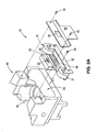
- the electron emitter assembly 10 is better illustrated in Figs. 2A and 2B , and includes a shaped cathode plate 20 with a cathode window 22.
- the cathode plate 20 surrounds and forms an enclosure around a filament 24 located adjacent the cathode window 22.
- the cathode plate 20 is mounted to a cathode assembly 26.
- An anode plate 28 with an anode window 30 is mounted to emitter block 50.
- the relative alignment of the cathode window 22, anode window 30 and filament 24 to each other is described later with reference to Fig. 6 .
- the cathode assembly 26 is mounted to the emitter block 50 by electrical insulator assemblies 31 and a mounting plate 35.
- the insulator assemblies 31, better illustrated in Fig. 2C electrically insulate the cathode assembly 26 from the emitter block 50 to which it is attached.
- Insulator assemblies 31 include an outer cup shaped HV shield 32, and an inner cup shaped HV shield 33, which are connected together in an overlapping fashion by an electrical insulator member 34.
- the open end of cup shaped shield 32 overlaps with the insulator member 34 and the open end of the inner cup shaped shield 33.
- the cathode assembly 26 includes two cathode blocks 36 and 38 separated by an air gap or insulating member 40, as illustrated in Fig. 2B .
- the filament 24 is mounted between the cathode blocks 36/38 by filament mounting plates 42/43.
- the cathode plate 20 is mounted to and is electrically connected with cathode block 36 by a screw 37. However, cathode plate 20 is electrically insulated from cathode block 38 by an insulator member 44 attached to the top of the cathode block 38.
- a pair of cathode leads 46 and 48 are attached to the cathode blocks 36 and 38 respectively.
- the emitter assembly 10 is mounted to the magnet assembly 12, which includes a emitter block 50 and a magnet support member 52, as illustrated in Figs. 2A and 3A . Screws 49 electrically connect the mounting plate 35 and anode plate 28 to the emitter block 50.
- the emitter block 50 includes an emitter recess 54 for housing the emitter assembly 10 and a crucible recess 56 into which the cathode leads 46/48 extend.
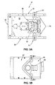
- the magnet support member 52 supports a pair of opposing magnet extension plates 60, with a magnet 62 extending therebetween at one end and the emitter assembly 10 and emitter block 50 disposed therebetween near the opposite end so as to create a magnetic field M around the emitter assembly 10 and emitter block 50 (see also Fig. 5 ).
- a pair of pole pieces 64 are attached to extension plates 60 and extend toward emitter block 50.
- a pair of auxiliary pole pieces 66 are attached to extension plates 60 and extend toward the anode plate 28.
- the pole pieces 64 and auxiliary pole pieces 66 act to shape the magnetic field M around emitter assembly 10 and crucible 58 for superior electron stream confinement as described in further detail below.
- a cover plate 67 over the magnet assembly 12 and another cover plate 68 over the emitter assembly 10 protect the E-gun from positive ions and other matter floating in the chamber, as illustrated in Fig. 3B .
- An aperture 69 is formed in the cover plate 68 through which the electron stream 100 flows.
- a crucible 58 is disposed in or above the recess 56.
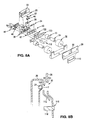
- the high voltage lead assembly 14 is best illustrated in Figs. 4A and 4B , and includes water lines 70 connected to mounting blocks 72, which are connected to inner and outer bellows 74 and 76 (preferably made of stainless steel), which are in turn connected to an insulator block 78.
- the mounting blocks 72 mount through holes in side wall 80 of a vapor deposition chamber to support the E-gun of the present invention.
- the mounting blocks 72, inner bellows 74 and insulator block 78 form a pair of wire channels 82 through which a pair of insulated wires 84/85 pass from outside the chamber to the insulator block 78.
- Water lines 70, mounting blocks 72, inner/outer bellows 47/76 and insulator block 78 form a water path 90, where cooling water enters through one of the water lines 70, passes through one of the mounting blocks 70, between one pair of inner/outer bellows 74/76, through the insulator block 78, and out through the other pair of inner/outer bellows 74/76, mounting block 72 and water line 70.
- Emitter block 50 is mounted to the top of insulator block 78 with a mounting plate 92 therebetween (see Fig. 1 ).
- a pair of adaptor blocks 94/95 connect between the high voltage leads 88/89 and the respective cathode leads 46/48.
- an adapter block 94/95 is illustrated in Fig. 3C, and includes a clamp member 96 that clamps to one of the high voltage leads 88/89, and a cathode lead socket 97 for receiving one of the cathode leads 46/48.
- An annular gold spring 98 can be used in socket 97 for making better electrical contact between the adaptor block 94/95 and the cathode lead 46/48 engaged therein.
- Cathode leads 46/48 removably plug into sockets 97 so that the emitter assembly 10 can be easily removed in its entirety for maintenance (such as replacing the filament 24).
- a voltage is placed on wire 84, that same voltage is present on lead 88, adaptor block 94, cathode lead 46, cathode block 36, cathode plate 20 and filament mounting plate 42, which are all electrically conductive and connected together.
- another voltage is placed on wire 85, that same voltage is present on lead 89, adaptor block 95, cathode lead 48, cathode block 38, and filament mounting plate 43, which are all electrically conductive and connected together.
- cooling water is circulated through water path 90.
- the flowing cooling water keeps the temperature of various E-gun elements at a safe temperature even if the chamber interior reaches temperatures that would otherwise destroy high-temperature intolerant elements.
- the flowing cooling water keeps the insulation around the wires 84/85 from being damaged by high temperatures. The presence of the insulation prevents arcing between the two wires 84/85 and ground.
- the cooling water also keeps the insulating block 78 and high voltage leads 88/89 from melting under the high chamber temperatures.
- a voltage V 1 is impressed onto wires 84 and 85 by the secondary winding of a 0-7 VAC iso-transformer. This allows the AC current through the filament to be raised and lowered while keeping the filament at a negative DC potential V 1 .
- the AC current flow through filament 24 raises the filament temperature and drives off electrons from the filament surface in all directions.
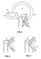
- An electrostatic field F is created by cathode plate 20 (which is at a voltage of V 1 ) and anode plate 28 (which is at system ground potential). Voltage V 1 is below the system ground potential to repel the electrons emitted by filament 24 through cathode window 22 and into a confined stream 100, as illustrated in Fig. 5 . The electrons in stream 100 are accelerated by the electrostatic field F until the electron stream 100 passes through anode window 30.
- the magnetic field M generated by the magnet assembly 12 and surrounding emitter assembly 10, induces a force on the moving electron stream 100 in a direction perpendicular to the direction of motion, thus causing the electron stream 100 to move in a circular path until the electrons strike the evaporant 102 in the crucible 58.
- the electron stream 100 incident on the crucible 58 evaporates the material 102 therein and forms a gas cloud in the chamber.
- cathode plate 20 and anode plate 28 The relative alignment of cathode plate 20 and anode plate 28 is illustrated in Fig. 6 .
- Cathode and anode plates 20/28 are spaced from each other to produce the electrostatic field F near filament 24.
- Cathode window 22 and anode window 30 are aligned to each other and to filament 24 to form an electrostatic lens for the electrons emitted by filament 24 and forming electron stream 100. Electrons emitted by filament 24 are trapped by cathode plate 20 and cathode blocks 36/38.
- Cathode window 22 is the only exit for these trapped electrons, which causes a more defined stream path for the electrons.
- the windows 22/30 need to be as small as possible to prevent ions from passing therethrough and damaging the filament, but not too small so as to impede the electrons in stream 100. Therefore, the sizes of the windows 22/30 are just slightly larger than filament 28 to freely allow electron stream 100 to pass therethrough.
- the upper edge 104 of anode window 30 is higher than the upper edge 106 of cathode window 22 by a predetermined amount to take into account the vertical displacement of the electrons caused by magnetic field M as the electrons travel between the cathode plate 20 and anode plate 28. Without this offset between window edges 104/106, the upper edge 104 of anode plate window 30 would block part of the electron stream 100 resulting in a scattered electron stream 100 and a burned anode plate 28.
- Arcing in the above described E-gun is prevented in several ways, which allows arc-free operation of the E-gun at much higher pressures.
- the focused electron stream 100 which is produced by the lensing effect of electrostatic field F and guided by the shaped magnetic field M, is maintained in a close parallel circular stream with a concentrated footprint as it strikes the crucible.
- cathode and anode plates 20/28 with windows 22/30 formed therein prevent positive ions, which are emitted from the evaporated material and directed back toward the electron emitter 10 by magnetic field M, from reaching and damaging the filament 24 and cathode plate 20. Since these ions have much greater mass than electrons, their radius of curvature under the influence of magnetic field M will be larger than that of the electron stream 100, making most of the ions strike the anode plate 28 below anode window 30.
- outer cup shaped HV shields 32 which are maintained at system ground potential along with mounting plate 35 and anode plate 28 mounted adjacent thereto, shield the insulator members 34 and inner cup shaped HV shields 33, which are held at a large negative electric potential, from the positive ions.
- the elements exposed to incoming positive ions are all at system ground (instead of significantly below system ground).
- cover plates 67 and 68 are placed over the magnetic assembly to prevent positive ions and other contaminants from accessing the emitter assembly 10.
- arcing between wires 84/85 is prevented by the presence of insulation layers around wires 84/85, the use of which is made possible by the cooling fluid flowing through water path 90. Otherwise, the insulation would be damaged and fail due to the extreme temperatures inside the chamber.
- the high voltages from wires 84/85 are not exposed to the chamber, except for at the cathode blocks 36 and filament 24, which are surrounded and protected by cathode plate 20. Surrounding the high voltage wires by the grounded, water cooled bellows prevents positive ions from collecting on the otherwise exposed high voltage wires.
- cathode window 22 is 0.10-0.15 cm (0.04-0.06 inches) taller, and 0.20-0.25 cm (0.08-0.1 inches) longer, than the height 0.32 cm (0.125 inches) and length 1.97 cm (0.775 inches) of filament 24.
- the anode plate 28 is spaced about 0.25 +/- 0.01 cm (0.100 +/- .005 inches) 0.051 cm from the cathode plate 20.
- the anode window is 0.216 - 0.241 cm (0.085-0.095 inches) taller, and 0.051 cm (0.020 inches) longer, than the height and length of cathode window 22.
- the upper edge 104 of anode window 30 is 0.191 cm (0.075 inches) higher than the upper edge 106 of cathode window 22 to accommodate the circular trajectory of the electron stream 100.
- an AC current of 0-7 VAC through the filament raises the filament 24 to 850-950°C to drive off electrons from the filament surface.
- the electrostatic field is approximately 4-10 KV. It has been found that the above described arc free E-gun can be run at pressures exceeding two orders of magnitude greater than conventional E-guns without incurring any arcing.
- Figure 7 illustrates an alternate embodiment of the present invention, which include an ion trap to attract positive ions incident on anode plate 28 away from anode window 30.
- a second anode window 110 is formed in anode plate 28, below window 30 and directly opposite flange portion 112 of cathode plate 20. The flange portion 112 of cathode plate 20 will attract positive ions through second window 110, thus reducing the number of ions that travel through window 30 and damage filament 24.
- FIGs 8A and 8B illustrate a second alternate embodiment of the present invention, where an ion trap plate 118 is attached to a mounting plate 120, which in turn is insulated from the filament mounting plate 43 by an insulator 122, but is electrically connected to the filament mounting plate 42.
- the anode plate 28 is mounted so that the ion trap plate 118 is aligned to the second anode window 110 (which includes aligned adjacent to, protruding into, or protruding through (as shown in Fig. 8B ) the anode window 10).
- the ion trap plate attracts positive ions through second window 110.
- a large quantity of positive ions are formed by the collision of highly energetic moving electrons and neutral molecules on the surface of the stationary target material and its evaporation vapor cloud.
- the vapor cloud composed of neutral atoms
- a large number of neutral atoms collide with the electron, loosing electrons from their outer shell, and become positively charged ions.
- the ions are immediately exposed to the magnetic field used to direct the electron stream.
- the ions move opposite to the stream of electrons, eventually striking the surface of the electron beam source filament, causing rapid erosion on its surface and hence limiting its performance and lifetime.
- the second anode window of Figs. 7 and 8A-B prevent such erosion.
- the negatively charged flange portion 112 of cathode plate 20 in Fig. 7 or the negatively charged ion trap plate 118 in 8A-B , attracts and neutralizes most of the positively charged ions impinging on its surface.
- the advantage of using the ion trap plate 118 of 8A-B instead of the flange portion 112 of Fig. 7 is that the ion trap plate can be made to better tolerate the incoming ions.
- inner and outer bellows 74 and 76 can instead be any type of water jacket member, rigid or not, that provides separate concentric or non-concentric wire channels 82 and water paths 90.
- the e-gun is described as being attached to a sidewall of the vacuum deposition chamber, the e-gun of the present invention can be disposed in any position inside the chamber.
- the voltage source supplying the various voltages discussed above could be a single voltage source device, or separate voltage source devices.
Landscapes
- Chemical & Material Sciences (AREA)
- Analytical Chemistry (AREA)
- Physics & Mathematics (AREA)
- Engineering & Computer Science (AREA)
- Plasma & Fusion (AREA)
- Electron Sources, Ion Sources (AREA)
- Physical Vapour Deposition (AREA)
Abstract
Description
- The present invention relates to electron gun apparatus.
-
JP 05-205678 DE 23 36 825 , andUS 4303694 describe electron gun apparatus of the kind comprising an electron emitter assembly including a filament that when heated emits electrons and a cathode plate disposed adjacent to the filament and forming a cathode window aligned to the filament, an anode plate disposed adjacent to the cathode plate and forming an anode window aligned to the cathode window, means for supporting a crucible, and a magnet assembly including a magnet adapted to generate a magnetic field for guiding an electron beam emitted by the filament into the mouth of the crucible when the cathode plate and the anode plate are connected to a voltage source that directs emitted electrons into a stream that traverses through the cathode window and the anode window in a direction 270° from the direction for entry into the mouth of the crucible. - Electron guns (E-guns) are used for various applications, and particularly for vapor deposition processes inside a sealed vacuum chamber. Such E-guns typically include an electron emitting source (emitter) for emitting a stream of electrons, high voltage leads to operate the emitter, a crucible for holding evaporant material, and a magnet for creating a magnetic field that directs the stream of electrons from the emitter onto the surface of the evaporant material. The incident electron stream evaporates the material to fill the chamber with a gaseous cloud for deposition onto substrates positioned in the chamber.
US Patents 3,710,072 and5,111,022 show various details of prior art E-guns. - One problem with such E-guns is arcing that occurs during operation, especially as the pressure inside the sealed vacuum chamber increases. More specifically, as the material in the crucible evaporates, a portion of it decomposes to positive ions plus some gas. These positive ions are emitted with a certain kinetic energy into the magnetic field, which guides the ions back toward the emitter along a similar path taken by the electron stream. Some of these ions can enter and damage the emitter.
- Another problem caused by the positive ions in the chamber involves the high voltage leads, which extend from the chamber wall to the E-gun. These leads are typically bare high voltage conductors. Positive ions floating in the chamber between these conductors can cause arcing between the conductors and ground. Minimizing sharp corners on the conductors does not completely solve this arcing problem. Further, it is difficult to electrically insulate these leads because most insulating materials cannot withstand the high chamber temperatures that exist during vapor deposition.
- One solution is proposed in
US Patent No. 5,216,690 (issued to Hanks ), in which a shield is added that surrounds all of the high voltage surfaces. The shield is grounded, and spaced from the HV surfaces by a distance that is below the mean free path of electrons at the highest pressure anticipated. The electrons making the transit, although accelerating quickly going from -KV cathode surface to nearby ground, have minimal ion collision probability over the entire distance. The electrons merely transfer to ground a minimal amount of energy. This suppresses arc-downs and glow discharges. However, the drawback to this type of E-gun is that the rigid ground shielded high voltage leads make it extremely difficult to install the device. - There is a need for an arc-free electron E-gun for vapor deposition processes.
-
US 3869675 describes electron gun apparatus of the kind defined hereinbefore at the beginning in which the filament is so enclosed within the electron emitter assembly that the cathode window provides the only exit for emitted electrons, the filament, the cathode window, and the anode window form an electrostatic lens in operation that produces a focussed electron beam exiting the anode window, the anode plate is attached to an emitter block having an emitter recess, and the filament and the cathode plate are housed in the emitter recess and mounted to the emitter block through electrically insulating means. - According to the present invention there is provided electron gun apparatus as defined by claim 1 hereinafter, reference to which should now be made.
- A preferred embodiment of the present invention solves the aforementioned problems by providing an E-gun with an improved electrostatic field, an improved magnetic field, and an improved flexible insulation on high voltage leads.
- In a preferred embodiment of the present invention, the magnet has a pair of poles that generates a magnetic field for guiding the electron stream along a path to the crucible, a pair of extension plates each extending from a different one of the poles of the magnet, and a plurality of extension members that extend from the extension plates toward the path of the electron stream. The magnet, pair of extension plates and plurality of extension members provide a uniform field along the electron stream path so that the electron stream is guided to the crucible with a minimum of divergence.
- In another preferred embodiment of the present invention, the electron gun includes an ion trap plate. The ion trap plate is electrically connectable to the voltage source. The anode plate includes an anode window formed therein that is aligned to the ion trap plate that attracts positive ions during operation.
- The invention will now be described by way of example with reference to the accompanying drawings, in which:
-
Fig. 1 is a partial exploded view of electron gun apparatus embodying the present invention. -
Fig. 2A is a partially exploded view of the emitter assembly and emitter block of the apparatus. -
Fig. 2B is an exploded view of the emitter assembly of the apparatus. -
Fig. 2C is a side cross-sectional view of the insulator assemblies of the apparatus. -
Fig. 3A is a top view of the magnet assembly of the apparatus. -
Fig. 3B is a top view of the magnet assembly with the cover plates in place. - Fig. 3C is an exploded view of the adapter block of the apparatus.
-
Fig. 4A is a top view of the high voltage lead assembly of the apparatus. -
Fig. 4B is a side cross-sectional view of the high voltage lead assembly of the apparatus. -
Fig. 5 is a partial side cross-section view of the emitter assembly and crucible of the apparatus. -
Fig. 6 is a partial side cross-section view of the emitter assembly of the apparatus. -
Fig. 7 is a partial side cross-section view of the emitter assembly of an alternative embodiment of the present invention. -
Fig. 8A is an exploded view of a second alternative embodiment of the present invention. -
Fig. 8B is a partial side cross-section view of the emitter assembly of the second alternative embodiment of the present invention. - An are-free electron gun (E-gun) for vapor deposition processes, which prevents arching by providing an improved electrostatic field, an improved magnetic field, and an improved insulation on high voltage leads, is illustrated in
Figs. 1 and3A , and includes anelectron emitter assembly 10, amagnet assembly 12, and a highvoltage lead assembly 14. - The
electron emitter assembly 10 is better illustrated inFigs. 2A and2B , and includes ashaped cathode plate 20 with acathode window 22. Thecathode plate 20 surrounds and forms an enclosure around afilament 24 located adjacent thecathode window 22. Thecathode plate 20 is mounted to acathode assembly 26. Ananode plate 28 with ananode window 30 is mounted toemitter block 50. The relative alignment of thecathode window 22,anode window 30 andfilament 24 to each other is described later with reference toFig. 6 . - The
cathode assembly 26 is mounted to theemitter block 50 by electrical insulator assemblies 31 and amounting plate 35. The insulator assemblies 31, better illustrated inFig. 2C , electrically insulate thecathode assembly 26 from theemitter block 50 to which it is attached.Insulator assemblies 31 include an outer cup shapedHV shield 32, and an inner cup shapedHV shield 33, which are connected together in an overlapping fashion by anelectrical insulator member 34. The open end of cup shapedshield 32 overlaps with theinsulator member 34 and the open end of the inner cup shapedshield 33. - The
cathode assembly 26 includes twocathode blocks member 40, as illustrated inFig. 2B . Thefilament 24 is mounted between the cathode blocks 36/38 byfilament mounting plates 42/43. Thecathode plate 20 is mounted to and is electrically connected withcathode block 36 by ascrew 37. However,cathode plate 20 is electrically insulated fromcathode block 38 by aninsulator member 44 attached to the top of thecathode block 38. A pair of cathode leads 46 and 48 are attached to the cathode blocks 36 and 38 respectively. - The
emitter assembly 10 is mounted to themagnet assembly 12, which includes aemitter block 50 and amagnet support member 52, as illustrated inFigs. 2A and3A .Screws 49 electrically connect the mountingplate 35 andanode plate 28 to theemitter block 50. Theemitter block 50 includes anemitter recess 54 for housing theemitter assembly 10 and acrucible recess 56 into which the cathode leads 46/48 extend. Themagnet support member 52 supports a pair of opposingmagnet extension plates 60, with amagnet 62 extending therebetween at one end and theemitter assembly 10 andemitter block 50 disposed therebetween near the opposite end so as to create a magnetic field M around theemitter assembly 10 and emitter block 50 (see alsoFig. 5 ). A pair ofpole pieces 64 are attached toextension plates 60 and extend towardemitter block 50. In addition, a pair ofauxiliary pole pieces 66 are attached toextension plates 60 and extend toward theanode plate 28. Thepole pieces 64 andauxiliary pole pieces 66 act to shape the magnetic field M aroundemitter assembly 10 andcrucible 58 for superior electron stream confinement as described in further detail below. Acover plate 67 over themagnet assembly 12 and anothercover plate 68 over theemitter assembly 10 protect the E-gun from positive ions and other matter floating in the chamber, as illustrated inFig. 3B . Anaperture 69 is formed in thecover plate 68 through which theelectron stream 100 flows. Acrucible 58 is disposed in or above therecess 56. - The high
voltage lead assembly 14 is best illustrated inFigs. 4A and 4B , and includeswater lines 70 connected to mountingblocks 72, which are connected to inner andouter bellows 74 and 76 (preferably made of stainless steel), which are in turn connected to aninsulator block 78. The mounting blocks 72 mount through holes inside wall 80 of a vapor deposition chamber to support the E-gun of the present invention. The mounting blocks 72, inner bellows 74 andinsulator block 78 form a pair ofwire channels 82 through which a pair ofinsulated wires 84/85 pass from outside the chamber to theinsulator block 78. From theinsulator block 78, thewires 84/85 pass upwards through insulator posts 86 (which are made of an electrically nonconducting material) and terminate at high voltage leads 88/89 respectively.Water lines 70, mountingblocks 72, inner/outer bellows 47/76 andinsulator block 78 form awater path 90, where cooling water enters through one of thewater lines 70, passes through one of the mounting blocks 70, between one pair of inner/outer bellows 74/76, through theinsulator block 78, and out through the other pair of inner/outer bellows 74/76, mountingblock 72 andwater line 70. -
Emitter block 50 is mounted to the top ofinsulator block 78 with a mountingplate 92 therebetween (seeFig. 1 ). A pair of adaptor blocks 94/95 connect between the high voltage leads 88/89 and the respective cathode leads 46/48. More specifically, anadapter block 94/95 is illustrated in Fig. 3C, and includes aclamp member 96 that clamps to one of the high voltage leads 88/89, and acathode lead socket 97 for receiving one of the cathode leads 46/48. Anannular gold spring 98 can be used insocket 97 for making better electrical contact between theadaptor block 94/95 and thecathode lead 46/48 engaged therein. Cathode leads 46/48 removably plug intosockets 97 so that theemitter assembly 10 can be easily removed in its entirety for maintenance (such as replacing the filament 24). - Assuming that the
chamber wall 80 is at system ground potential, then so too are mountingblocks 72, bellows 74/76,insulator block 78, mountingplate 92,emitter block 50 andanode plate 28, which are all made of conductive metal and electrically connected together. Assuming a voltage is placed onwire 84, that same voltage is present onlead 88,adaptor block 94,cathode lead 46,cathode block 36,cathode plate 20 andfilament mounting plate 42, which are all electrically conductive and connected together. Assuming another voltage is placed onwire 85, that same voltage is present onlead 89,adaptor block 95,cathode lead 48,cathode block 38, andfilament mounting plate 43, which are all electrically conductive and connected together. - During operation, cooling water is circulated through
water path 90. The flowing cooling water keeps the temperature of various E-gun elements at a safe temperature even if the chamber interior reaches temperatures that would otherwise destroy high-temperature intolerant elements. For example, the flowing cooling water keeps the insulation around thewires 84/85 from being damaged by high temperatures. The presence of the insulation prevents arcing between the twowires 84/85 and ground. The cooling water also keeps the insulatingblock 78 and high voltage leads 88/89 from melting under the high chamber temperatures. - To create a stream of electrons for evaporating the material in the
crucible 58, a voltage V1 is impressed ontowires filament 24 raises the filament temperature and drives off electrons from the filament surface in all directions. - An electrostatic field F is created by cathode plate 20 (which is at a voltage of V1) and anode plate 28 (which is at system ground potential). Voltage V1 is below the system ground potential to repel the electrons emitted by
filament 24 throughcathode window 22 and into a confinedstream 100, as illustrated inFig. 5 . The electrons instream 100 are accelerated by the electrostatic field F until theelectron stream 100 passes throughanode window 30. - The magnetic field M, generated by the
magnet assembly 12 and surroundingemitter assembly 10, induces a force on the movingelectron stream 100 in a direction perpendicular to the direction of motion, thus causing theelectron stream 100 to move in a circular path until the electrons strike theevaporant 102 in thecrucible 58. Theelectron stream 100 incident on thecrucible 58 evaporates the material 102 therein and forms a gas cloud in the chamber. - The relative alignment of
cathode plate 20 andanode plate 28 is illustrated inFig. 6 . Cathode andanode plates 20/28 are spaced from each other to produce the electrostatic field F nearfilament 24.Cathode window 22 andanode window 30 are aligned to each other and to filament 24 to form an electrostatic lens for the electrons emitted byfilament 24 and formingelectron stream 100. Electrons emitted byfilament 24 are trapped bycathode plate 20 and cathode blocks 36/38.Cathode window 22 is the only exit for these trapped electrons, which causes a more defined stream path for the electrons. - The
windows 22/30 need to be as small as possible to prevent ions from passing therethrough and damaging the filament, but not too small so as to impede the electrons instream 100. Therefore, the sizes of thewindows 22/30 are just slightly larger thanfilament 28 to freely allowelectron stream 100 to pass therethrough. In addition, theupper edge 104 ofanode window 30 is higher than theupper edge 106 ofcathode window 22 by a predetermined amount to take into account the vertical displacement of the electrons caused by magnetic field M as the electrons travel between thecathode plate 20 andanode plate 28. Without this offset between window edges 104/106, theupper edge 104 ofanode plate window 30 would block part of theelectron stream 100 resulting in ascattered electron stream 100 and a burnedanode plate 28. - Arcing in the above described E-gun is prevented in several ways, which allows arc-free operation of the E-gun at much higher pressures. First, the lensing effect of the cathode/
anode windows 22/30 produces afocused electron stream 100 exiting theanode window 30. Second,auxiliary pole pieces 66 andpole pieces 64 are positioned along the electron stream path, thus providing a concentrated and uniform magnetic field along the width of theelectron stream 100 to minimize any divergence thereof. Thefocused electron stream 100, which is produced by the lensing effect of electrostatic field F and guided by the shaped magnetic field M, is maintained in a close parallel circular stream with a concentrated footprint as it strikes the crucible. Third, cathode andanode plates 20/28 withwindows 22/30 formed therein prevent positive ions, which are emitted from the evaporated material and directed back toward theelectron emitter 10 by magnetic field M, from reaching and damaging thefilament 24 andcathode plate 20. Since these ions have much greater mass than electrons, their radius of curvature under the influence of magnetic field M will be larger than that of theelectron stream 100, making most of the ions strike theanode plate 28 belowanode window 30. Fourth, outer cup shaped HV shields 32, which are maintained at system ground potential along with mountingplate 35 andanode plate 28 mounted adjacent thereto, shield theinsulator members 34 and inner cup shaped HV shields 33, which are held at a large negative electric potential, from the positive ions. Thus, the elements exposed to incoming positive ions (anode plate 28, mountingplate 35, HV shields 32 and emitter block 50) are all at system ground (instead of significantly below system ground). Fifth,cover plates emitter assembly 10. Sixth, arcing betweenwires 84/85 is prevented by the presence of insulation layers aroundwires 84/85, the use of which is made possible by the cooling fluid flowing throughwater path 90. Otherwise, the insulation would be damaged and fail due to the extreme temperatures inside the chamber. Seventh, the high voltages fromwires 84/85 are not exposed to the chamber, except for at the cathode blocks 36 andfilament 24, which are surrounded and protected bycathode plate 20. Surrounding the high voltage wires by the grounded, water cooled bellows prevents positive ions from collecting on the otherwise exposed high voltage wires. - An arc free E-gun according to the present invention has been developed, where the
cathode window 22 is 0.10-0.15 cm (0.04-0.06 inches) taller, and 0.20-0.25 cm (0.08-0.1 inches) longer, than the height 0.32 cm (0.125 inches) and length 1.97 cm (0.775 inches) offilament 24. Theanode plate 28 is spaced about 0.25 +/- 0.01 cm (0.100 +/- .005 inches) 0.051 cm from thecathode plate 20. The anode window is 0.216 - 0.241 cm (0.085-0.095 inches) taller, and 0.051 cm (0.020 inches) longer, than the height and length ofcathode window 22. Theupper edge 104 ofanode window 30 is 0.191 cm (0.075 inches) higher than theupper edge 106 ofcathode window 22 to accommodate the circular trajectory of theelectron stream 100. During operation, an AC current of 0-7 VAC through the filament raises thefilament 24 to 850-950°C to drive off electrons from the filament surface. The electrostatic field is approximately 4-10 KV. It has been found that the above described arc free E-gun can be run at pressures exceeding two orders of magnitude greater than conventional E-guns without incurring any arcing. -
Figure 7 illustrates an alternate embodiment of the present invention, which include an ion trap to attract positive ions incident onanode plate 28 away fromanode window 30. Asecond anode window 110 is formed inanode plate 28, belowwindow 30 and directly oppositeflange portion 112 ofcathode plate 20. Theflange portion 112 ofcathode plate 20 will attract positive ions throughsecond window 110, thus reducing the number of ions that travel throughwindow 30 anddamage filament 24. -
Figures 8A and 8B illustrate a second alternate embodiment of the present invention, where anion trap plate 118 is attached to a mountingplate 120, which in turn is insulated from thefilament mounting plate 43 by aninsulator 122, but is electrically connected to thefilament mounting plate 42. Theanode plate 28 is mounted so that theion trap plate 118 is aligned to the second anode window 110 (which includes aligned adjacent to, protruding into, or protruding through (as shown inFig. 8B ) the anode window 10). The ion trap plate attracts positive ions throughsecond window 110. - During the process of manufacturing optical thin films in a vacuum chamber, a large quantity of positive ions are formed by the collision of highly energetic moving electrons and neutral molecules on the surface of the stationary target material and its evaporation vapor cloud. As the vapor cloud, composed of neutral atoms, propagates through the path of the electron stream, a large number of neutral atoms collide with the electron, loosing electrons from their outer shell, and become positively charged ions. The ions are immediately exposed to the magnetic field used to direct the electron stream. The ions move opposite to the stream of electrons, eventually striking the surface of the electron beam source filament, causing rapid erosion on its surface and hence limiting its performance and lifetime. The second anode window of
Figs. 7 and8A-B prevent such erosion. The negatively chargedflange portion 112 ofcathode plate 20 inFig. 7 , or the negatively chargedion trap plate 118 in8A-B , attracts and neutralizes most of the positively charged ions impinging on its surface. The advantage of using theion trap plate 118 of8A-B instead of theflange portion 112 ofFig. 7 is that the ion trap plate can be made to better tolerate the incoming ions. - It is to be understood that the present invention is not limited to the embodiment described above and illustrated herein, but encompasses any and all variations falling within the scope of the appended claims. For example, inner and
outer bellows non-concentric wire channels 82 andwater paths 90. In addition, while the e-gun is described as being attached to a sidewall of the vacuum deposition chamber, the e-gun of the present invention can be disposed in any position inside the chamber. Further, the voltage source supplying the various voltages discussed above could be a single voltage source device, or separate voltage source devices.
Claims (2)
- Electron gun apparatus comprising:an electron emitter assembly (10) including a filament (24) that when heated emits electrons and a cathode plate (20) disposed adjacent to the filament (24) and forming a cathode window (22) aligned to the filament (24);an anode plate (28) disposed adjacent to the cathode plate (20) and forming an anode window (30) aligned to the cathode window (22);means for supporting a crucible; anda magnet assembly (12) including a magnet (62) adapted to generate a magnetic field for guiding an electron beam emitted by the filament (24) into the mouth of the crucible when the cathode plate (20) and the anode plate (28) are connected to a voltage source that directs emitted electrons into a stream that traverses through the cathode window (22) and the anode window (30) in a direction 270° from the direction for entry into the mouth of the crucible,the filament (24) being so enclosed within the electron emitter assembly (10) that the cathode window (22) provides the only exit for emitted electrons;the filament (24), the cathode window (22), and the anode window (30) forming an electrostatic lens in operation that produces a focussed electron beam exiting the anode window (30);the anode plate (28) being attached to an emitter block (50) having an emitter recess (54); andthe filament (24) and the cathode plate (20) being housed in the emitter recess (54) and mounted to the emitter block (50) through electrically insulating means(31),characterised by a pair of insulated wires (84, 85) electrically connected to the filament (24) for passing electrical current through and heating the filament (24), and a cooling fluid jacket (76) that forms a first channel (82) through which at least part of one of the wires passes and a second channel (90) through which a cooling fluid flows.
- Electron gun apparatus according to claim 1, characterised in that the cooling jacket includes a first bellows (74) forming the first channel (82), and a second bellows (76) concentrically surrounding the first bellows (74), the second channel (90) being formed between the first and second bellows (74, 76).
Applications Claiming Priority (3)
| Application Number | Priority Date | Filing Date | Title |
|---|---|---|---|
| US09/283,898 US6064686A (en) | 1999-03-30 | 1999-03-30 | Arc-free electron gun |
| US283898 | 1999-03-30 | ||
| PCT/US2000/006015 WO2000058049A1 (en) | 1999-03-30 | 2000-03-08 | Arc-free electron gun |
Publications (3)
| Publication Number | Publication Date |
|---|---|
| EP1204507A1 EP1204507A1 (en) | 2002-05-15 |
| EP1204507A4 EP1204507A4 (en) | 2007-07-18 |
| EP1204507B1 true EP1204507B1 (en) | 2010-01-13 |
Family
ID=23088048
Family Applications (1)
| Application Number | Title | Priority Date | Filing Date |
|---|---|---|---|
| EP00914863A Expired - Lifetime EP1204507B1 (en) | 1999-03-30 | 2000-03-08 | Arc-free electron gun |
Country Status (9)
| Country | Link |
|---|---|
| US (1) | US6064686A (en) |
| EP (1) | EP1204507B1 (en) |
| JP (1) | JP4689049B2 (en) |
| KR (1) | KR100711529B1 (en) |
| AT (1) | ATE454948T1 (en) |
| AU (1) | AU3619600A (en) |
| DE (1) | DE60043700D1 (en) |
| TW (1) | TW451249B (en) |
| WO (1) | WO2000058049A1 (en) |
Families Citing this family (9)
| Publication number | Priority date | Publication date | Assignee | Title |
|---|---|---|---|---|
| JP2004192903A (en) * | 2002-12-10 | 2004-07-08 | Prazmatec:Kk | Electron gun |
| JP4584008B2 (en) * | 2005-04-14 | 2010-11-17 | 浜松ホトニクス株式会社 | Electron beam assisted irradiation laser ablation deposition system |
| US7544523B2 (en) * | 2005-12-23 | 2009-06-09 | Fei Company | Method of fabricating nanodevices |
| KR100787168B1 (en) * | 2006-02-10 | 2007-12-21 | (주)인텍 | Electron beam generator |
| US7764008B2 (en) * | 2006-02-24 | 2010-07-27 | Ferrotec (Usa) Corporation | Electron beam gun |
| US8024149B2 (en) * | 2006-08-03 | 2011-09-20 | Titanium Metals Corporation | Overheat detection system |
| KR100964094B1 (en) * | 2008-11-10 | 2010-06-16 | 포항공과대학교 산학협력단 | Femtosecond Electron Beam Generator |
| CN101712091B (en) * | 2009-10-23 | 2012-08-29 | 江苏达胜加速器制造有限公司 | Electronic gun cover plate assembling mold and assembling method |
| DE102020213174B4 (en) | 2020-10-19 | 2026-01-08 | THEVA DüNNSCHICHTTECHNIK GMBH | EMITE ARRAY FOR AN ELECTRON GUN, ACTIVELY COOLED BEAM GUIDE AND AXIAL ELECTRON GUN |
Family Cites Families (26)
| Publication number | Priority date | Publication date | Assignee | Title |
|---|---|---|---|---|
| GB85458A (en) * | 1958-05-05 | |||
| US3177535A (en) * | 1960-06-21 | 1965-04-13 | Stauffer Chemical Co | Electron beam furnace with low beam source |
| US3286021A (en) * | 1965-06-01 | 1966-11-15 | Temescal Metallurgical Corp | Cable terminal for use with electron gun apparatus |
| US3535428A (en) * | 1968-07-17 | 1970-10-20 | Air Reduction | Apparatus for producing and directing an electron beam |
| DE1934327A1 (en) * | 1968-11-22 | 1970-06-04 | Inst Elektronische Bauelemente | Thin film prodn by ion sputtering method |
| US3582529A (en) * | 1969-09-24 | 1971-06-01 | Air Reduction | Electron beam heating apparatus and control system therein |
| US3710072A (en) * | 1971-05-10 | 1973-01-09 | Airco Inc | Vapor source assembly |
| GB1361771A (en) | 1972-02-15 | 1974-07-30 | Leybold Heraeus Verwaltung | Apparatus for heating material by means of a electron beam in a vacuum |
| US3801719A (en) * | 1973-01-18 | 1974-04-02 | Western Electric Co | Emitter block assembly |
| DE2336825B2 (en) | 1973-07-19 | 1976-08-05 | Siemens AG, 1000 Berlin und 8000 München | METHOD AND DEVICE FOR TEMPERING A SUBSTRATE CARRYING VAPORIZED COATINGS |
| US3883679A (en) * | 1973-08-08 | 1975-05-13 | Airco Inc | Vapor source assembly |
| US4064352A (en) * | 1976-02-17 | 1977-12-20 | Varian Associates, Inc. | Electron beam evaporator having beam spot control |
| FR2455634A1 (en) * | 1979-05-04 | 1980-11-28 | Bois Daniel | METHOD AND DEVICE FOR VACUUM EVAPORATION DEPOSITION USING A MOLDED ELECTRON BEAM AND A SCREEN |
| JPS5966847U (en) * | 1982-10-28 | 1984-05-04 | 日本電子株式会社 | electron gun |
| JPS624862A (en) * | 1985-06-29 | 1987-01-10 | Anelva Corp | Electron gun for vacuum deposition |
| JPH0256840A (en) * | 1988-08-22 | 1990-02-26 | Toshiba Corp | electron gun device |
| US5111022A (en) * | 1989-08-23 | 1992-05-05 | Tfi Telemark | Cooling system for electron beam gun and method |
| JP2959022B2 (en) * | 1990-02-15 | 1999-10-06 | 日本電気株式会社 | Ion trap |
| JPH04106849A (en) * | 1990-08-24 | 1992-04-08 | Mitsubishi Electric Corp | Processing apparatus |
| JPH04363847A (en) * | 1991-06-11 | 1992-12-16 | Mitsubishi Heavy Ind Ltd | Electron gun |
| US5182488A (en) * | 1991-08-27 | 1993-01-26 | The Boc Group, Inc. | Electron beam gun for use in an electron beam evaporation source |
| JPH05205678A (en) | 1992-01-24 | 1993-08-13 | Mitsubishi Heavy Ind Ltd | Linear electron gun |
| US5216690A (en) * | 1992-03-11 | 1993-06-01 | Hanks Charles W | Electron beam gun with grounded shield to prevent arc down |
| US5418348A (en) * | 1992-10-29 | 1995-05-23 | Mdc Vacuum Products, Inc. | Electron beam source assembly |
| US5338913A (en) * | 1992-12-28 | 1994-08-16 | Tfi Telemark | Electron beam gun with liquid cooled rotatable crucible |
| JPH0890256A (en) * | 1994-09-19 | 1996-04-09 | Hitachi Ltd | Article processing correction device |
-
1999
- 1999-03-30 US US09/283,898 patent/US6064686A/en not_active Expired - Lifetime
-
2000
- 2000-03-08 KR KR20017012316A patent/KR100711529B1/en not_active Expired - Fee Related
- 2000-03-08 WO PCT/US2000/006015 patent/WO2000058049A1/en not_active Ceased
- 2000-03-08 JP JP2000607788A patent/JP4689049B2/en not_active Expired - Fee Related
- 2000-03-08 DE DE60043700T patent/DE60043700D1/en not_active Expired - Lifetime
- 2000-03-08 EP EP00914863A patent/EP1204507B1/en not_active Expired - Lifetime
- 2000-03-08 AU AU36196/00A patent/AU3619600A/en not_active Abandoned
- 2000-03-08 AT AT00914863T patent/ATE454948T1/en not_active IP Right Cessation
- 2000-05-02 TW TW089105781A patent/TW451249B/en not_active IP Right Cessation
Also Published As
| Publication number | Publication date |
|---|---|
| ATE454948T1 (en) | 2010-01-15 |
| KR20020006531A (en) | 2002-01-19 |
| DE60043700D1 (en) | 2010-03-04 |
| AU3619600A (en) | 2000-10-16 |
| WO2000058049A1 (en) | 2000-10-05 |
| JP2002540574A (en) | 2002-11-26 |
| US6064686A (en) | 2000-05-16 |
| JP4689049B2 (en) | 2011-05-25 |
| KR100711529B1 (en) | 2007-04-27 |
| TW451249B (en) | 2001-08-21 |
| EP1204507A1 (en) | 2002-05-15 |
| EP1204507A4 (en) | 2007-07-18 |
Similar Documents
| Publication | Publication Date | Title |
|---|---|---|
| KR100346863B1 (en) | Endcap for indirectly heated cathode of ion source | |
| CA1048171A (en) | Electron discharge device | |
| US6271529B1 (en) | Ion implantation with charge neutralization | |
| EP0324247B1 (en) | Ion implantation surface charge control method and apparatus | |
| TWI457967B (en) | Ion source with adjustable aperture used in creaing ion beam and related method | |
| CA1321229C (en) | Electron cyclotron resonance ion source | |
| JP2010080446A (en) | Extraction electrode manipulator system, and ion implantation system | |
| JP2008518407A (en) | Ionizer and method for gas cluster ion beam formation | |
| JP2003503819A (en) | Ion beam generator | |
| US8796649B2 (en) | Ion implanter | |
| US7102139B2 (en) | Source arc chamber for ion implanter having repeller electrode mounted to external insulator | |
| US6064686A (en) | Arc-free electron gun | |
| US4716340A (en) | Pre-ionization aided sputter gun | |
| EP0690473A2 (en) | Ion beam electron neutralizer | |
| US3450824A (en) | Method and apparatus for producing and directing an electron beam | |
| US5418348A (en) | Electron beam source assembly | |
| US7304319B2 (en) | Wafer charge compensation device and ion implantation system having the same | |
| US9721760B2 (en) | Electron beam plasma source with reduced metal contamination | |
| JP2913186B2 (en) | Ion source device | |
| TWI850898B (en) | Toroidal motion enhanced ion source | |
| JPH05182623A (en) | Ion implantation device and method of lengthening lifetime of ion source | |
| JPH08102278A (en) | Ion beam generator and method | |
| JP5222286B2 (en) | Magnetic analysis apparatus and method for ion implantation | |
| TW201503208A (en) | Flourine and HF resistant seals for an ion source | |
| CN114360991A (en) | Carbon ion source device with reflector power supply |
Legal Events
| Date | Code | Title | Description |
|---|---|---|---|
| PUAI | Public reference made under article 153(3) epc to a published international application that has entered the european phase |
Free format text: ORIGINAL CODE: 0009012 |
|
| 17P | Request for examination filed |
Effective date: 20011015 |
|
| AK | Designated contracting states |
Kind code of ref document: A1 Designated state(s): AT BE CH CY DE DK ES FI FR GB GR IE IT LI LU MC NL PT SE |
|
| A4 | Supplementary search report drawn up and despatched |
Effective date: 20070619 |
|
| 17Q | First examination report despatched |
Effective date: 20070927 |
|
| GRAP | Despatch of communication of intention to grant a patent |
Free format text: ORIGINAL CODE: EPIDOSNIGR1 |
|
| GRAS | Grant fee paid |
Free format text: ORIGINAL CODE: EPIDOSNIGR3 |
|
| GRAA | (expected) grant |
Free format text: ORIGINAL CODE: 0009210 |
|
| AK | Designated contracting states |
Kind code of ref document: B1 Designated state(s): AT BE CH CY DE DK ES FI FR GB GR IE IT LI LU MC NL PT SE |
|
| REG | Reference to a national code |
Ref country code: GB Ref legal event code: FG4D |
|
| REG | Reference to a national code |
Ref country code: CH Ref legal event code: EP |
|
| REG | Reference to a national code |
Ref country code: IE Ref legal event code: FG4D |
|
| REF | Corresponds to: |
Ref document number: 60043700 Country of ref document: DE Date of ref document: 20100304 Kind code of ref document: P |
|
| REG | Reference to a national code |
Ref country code: NL Ref legal event code: VDEP Effective date: 20100113 |
|
| PG25 | Lapsed in a contracting state [announced via postgrant information from national office to epo] |
Ref country code: AT Free format text: LAPSE BECAUSE OF FAILURE TO SUBMIT A TRANSLATION OF THE DESCRIPTION OR TO PAY THE FEE WITHIN THE PRESCRIBED TIME-LIMIT Effective date: 20100113 |
|
| RAP2 | Party data changed (patent owner data changed or rights of a patent transferred) |
Owner name: TFI TELEMARK |
|
| PG25 | Lapsed in a contracting state [announced via postgrant information from national office to epo] |
Ref country code: PT Free format text: LAPSE BECAUSE OF FAILURE TO SUBMIT A TRANSLATION OF THE DESCRIPTION OR TO PAY THE FEE WITHIN THE PRESCRIBED TIME-LIMIT Effective date: 20100513 Ref country code: NL Free format text: LAPSE BECAUSE OF FAILURE TO SUBMIT A TRANSLATION OF THE DESCRIPTION OR TO PAY THE FEE WITHIN THE PRESCRIBED TIME-LIMIT Effective date: 20100113 Ref country code: ES Free format text: LAPSE BECAUSE OF FAILURE TO SUBMIT A TRANSLATION OF THE DESCRIPTION OR TO PAY THE FEE WITHIN THE PRESCRIBED TIME-LIMIT Effective date: 20100424 |
|
| PG25 | Lapsed in a contracting state [announced via postgrant information from national office to epo] |
Ref country code: FI Free format text: LAPSE BECAUSE OF FAILURE TO SUBMIT A TRANSLATION OF THE DESCRIPTION OR TO PAY THE FEE WITHIN THE PRESCRIBED TIME-LIMIT Effective date: 20100113 |
|
| PG25 | Lapsed in a contracting state [announced via postgrant information from national office to epo] |
Ref country code: MC Free format text: LAPSE BECAUSE OF NON-PAYMENT OF DUE FEES Effective date: 20100331 Ref country code: GR Free format text: LAPSE BECAUSE OF FAILURE TO SUBMIT A TRANSLATION OF THE DESCRIPTION OR TO PAY THE FEE WITHIN THE PRESCRIBED TIME-LIMIT Effective date: 20100414 Ref country code: CY Free format text: LAPSE BECAUSE OF FAILURE TO SUBMIT A TRANSLATION OF THE DESCRIPTION OR TO PAY THE FEE WITHIN THE PRESCRIBED TIME-LIMIT Effective date: 20100113 Ref country code: BE Free format text: LAPSE BECAUSE OF FAILURE TO SUBMIT A TRANSLATION OF THE DESCRIPTION OR TO PAY THE FEE WITHIN THE PRESCRIBED TIME-LIMIT Effective date: 20100113 Ref country code: SE Free format text: LAPSE BECAUSE OF FAILURE TO SUBMIT A TRANSLATION OF THE DESCRIPTION OR TO PAY THE FEE WITHIN THE PRESCRIBED TIME-LIMIT Effective date: 20100113 |
|
| REG | Reference to a national code |
Ref country code: CH Ref legal event code: PL |
|
| PLBE | No opposition filed within time limit |
Free format text: ORIGINAL CODE: 0009261 |
|
| STAA | Information on the status of an ep patent application or granted ep patent |
Free format text: STATUS: NO OPPOSITION FILED WITHIN TIME LIMIT |
|
| 26N | No opposition filed |
Effective date: 20101014 |
|
| REG | Reference to a national code |
Ref country code: FR Ref legal event code: CA |
|
| PG25 | Lapsed in a contracting state [announced via postgrant information from national office to epo] |
Ref country code: IE Free format text: LAPSE BECAUSE OF NON-PAYMENT OF DUE FEES Effective date: 20100308 Ref country code: DK Free format text: LAPSE BECAUSE OF FAILURE TO SUBMIT A TRANSLATION OF THE DESCRIPTION OR TO PAY THE FEE WITHIN THE PRESCRIBED TIME-LIMIT Effective date: 20100113 |
|
| PG25 | Lapsed in a contracting state [announced via postgrant information from national office to epo] |
Ref country code: CH Free format text: LAPSE BECAUSE OF NON-PAYMENT OF DUE FEES Effective date: 20100331 Ref country code: LI Free format text: LAPSE BECAUSE OF NON-PAYMENT OF DUE FEES Effective date: 20100331 |
|
| PGFP | Annual fee paid to national office [announced via postgrant information from national office to epo] |
Ref country code: IT Payment date: 20120328 Year of fee payment: 13 |
|
| PG25 | Lapsed in a contracting state [announced via postgrant information from national office to epo] |
Ref country code: LU Free format text: LAPSE BECAUSE OF NON-PAYMENT OF DUE FEES Effective date: 20100308 |
|
| PGFP | Annual fee paid to national office [announced via postgrant information from national office to epo] |
Ref country code: GB Payment date: 20130306 Year of fee payment: 14 Ref country code: FR Payment date: 20130325 Year of fee payment: 14 |
|
| REG | Reference to a national code |
Ref country code: DE Ref legal event code: R082 Ref document number: 60043700 Country of ref document: DE Representative=s name: PATENTANWAELTE BETTEN & RESCH, DE Ref country code: DE Ref legal event code: R082 Ref document number: 60043700 Country of ref document: DE Representative=s name: BETTEN & RESCH PATENT- UND RECHTSANWAELTE PART, DE |
|
| GBPC | Gb: european patent ceased through non-payment of renewal fee |
Effective date: 20140308 |
|
| REG | Reference to a national code |
Ref country code: FR Ref legal event code: ST Effective date: 20141128 |
|
| PG25 | Lapsed in a contracting state [announced via postgrant information from national office to epo] |
Ref country code: GB Free format text: LAPSE BECAUSE OF NON-PAYMENT OF DUE FEES Effective date: 20140308 Ref country code: FR Free format text: LAPSE BECAUSE OF NON-PAYMENT OF DUE FEES Effective date: 20140331 |
|
| PG25 | Lapsed in a contracting state [announced via postgrant information from national office to epo] |
Ref country code: IT Free format text: LAPSE BECAUSE OF NON-PAYMENT OF DUE FEES Effective date: 20140308 |
|
| PGFP | Annual fee paid to national office [announced via postgrant information from national office to epo] |
Ref country code: DE Payment date: 20180403 Year of fee payment: 19 |
|
| REG | Reference to a national code |
Ref country code: DE Ref legal event code: R119 Ref document number: 60043700 Country of ref document: DE |
|
| PG25 | Lapsed in a contracting state [announced via postgrant information from national office to epo] |
Ref country code: DE Free format text: LAPSE BECAUSE OF NON-PAYMENT OF DUE FEES Effective date: 20191001 |