EP1204303A2 - Cladded material construction for etched-tri-metal circuits - Google Patents
Cladded material construction for etched-tri-metal circuits Download PDFInfo
- Publication number
- EP1204303A2 EP1204303A2 EP01125894A EP01125894A EP1204303A2 EP 1204303 A2 EP1204303 A2 EP 1204303A2 EP 01125894 A EP01125894 A EP 01125894A EP 01125894 A EP01125894 A EP 01125894A EP 1204303 A2 EP1204303 A2 EP 1204303A2
- Authority
- EP
- European Patent Office
- Prior art keywords
- tri
- metal
- cladding
- layer
- layers
- Prior art date
- Legal status (The legal status is an assumption and is not a legal conclusion. Google has not performed a legal analysis and makes no representation as to the accuracy of the status listed.)
- Granted
Links
Images

Classifications
-
- H—ELECTRICITY
- H05—ELECTRIC TECHNIQUES NOT OTHERWISE PROVIDED FOR
- H05K—PRINTED CIRCUITS; CASINGS OR CONSTRUCTIONAL DETAILS OF ELECTRIC APPARATUS; MANUFACTURE OF ASSEMBLAGES OF ELECTRICAL COMPONENTS
- H05K3/00—Apparatus or processes for manufacturing printed circuits
- H05K3/02—Apparatus or processes for manufacturing printed circuits in which the conductive material is applied to the surface of the insulating support and is thereafter removed from such areas of the surface which are not intended for current conducting or shielding
- H05K3/022—Processes for manufacturing precursors of printed circuits, i.e. copper-clad substrates
-
- B—PERFORMING OPERATIONS; TRANSPORTING
- B32—LAYERED PRODUCTS
- B32B—LAYERED PRODUCTS, i.e. PRODUCTS BUILT-UP OF STRATA OF FLAT OR NON-FLAT, e.g. CELLULAR OR HONEYCOMB, FORM
- B32B15/00—Layered products comprising a layer of metal
- B32B15/01—Layered products comprising a layer of metal all layers being exclusively metallic
- B32B15/017—Layered products comprising a layer of metal all layers being exclusively metallic one layer being formed of aluminium or an aluminium alloy, another layer being formed of an alloy based on a non ferrous metal other than aluminium
-
- B—PERFORMING OPERATIONS; TRANSPORTING
- B32—LAYERED PRODUCTS
- B32B—LAYERED PRODUCTS, i.e. PRODUCTS BUILT-UP OF STRATA OF FLAT OR NON-FLAT, e.g. CELLULAR OR HONEYCOMB, FORM
- B32B15/00—Layered products comprising a layer of metal
- B32B15/01—Layered products comprising a layer of metal all layers being exclusively metallic
- B32B15/018—Layered products comprising a layer of metal all layers being exclusively metallic one layer being formed of a noble metal or a noble metal alloy
-
- H—ELECTRICITY
- H05—ELECTRIC TECHNIQUES NOT OTHERWISE PROVIDED FOR
- H05K—PRINTED CIRCUITS; CASINGS OR CONSTRUCTIONAL DETAILS OF ELECTRIC APPARATUS; MANUFACTURE OF ASSEMBLAGES OF ELECTRICAL COMPONENTS
- H05K2201/00—Indexing scheme relating to printed circuits covered by H05K1/00
- H05K2201/03—Conductive materials
- H05K2201/0332—Structure of the conductor
- H05K2201/0335—Layered conductors or foils
- H05K2201/0361—Etched tri-metal structure, i.e. metal layers or metal patterns on both sides of a different central metal layer which is later at least partly etched
-
- Y—GENERAL TAGGING OF NEW TECHNOLOGICAL DEVELOPMENTS; GENERAL TAGGING OF CROSS-SECTIONAL TECHNOLOGIES SPANNING OVER SEVERAL SECTIONS OF THE IPC; TECHNICAL SUBJECTS COVERED BY FORMER USPC CROSS-REFERENCE ART COLLECTIONS [XRACs] AND DIGESTS
- Y10—TECHNICAL SUBJECTS COVERED BY FORMER USPC
- Y10T—TECHNICAL SUBJECTS COVERED BY FORMER US CLASSIFICATION
- Y10T29/00—Metal working
- Y10T29/49—Method of mechanical manufacture
- Y10T29/49002—Electrical device making
- Y10T29/49117—Conductor or circuit manufacturing
- Y10T29/49124—On flat or curved insulated base, e.g., printed circuit, etc.
- Y10T29/49126—Assembling bases
Definitions
- This invention relates generally to circuit boards and more particularly to a material construction for use in Etched-Tri-Metal, "ETM", multi-layer circuit boards.
- a method for cladding material for etched-tri-metal circuits to maintain the dimensional tolerance and reducing the stresses in the cladded material having the steps of first forming a stacked set of tri-metal material having three layers of metal.
- the central layer is one material, which is aluminum, and the top and bottom layers are a second material, which are copper.
- each set of the tri-metal material have the outside surfaces of the top and bottom layers oxidized to prevent the sets from adhering together when they are stacked.
- each set Prior to being stacked, each set is fed through a cladding mill having a predetermined pressure and temperature. After exiting the cladding mill, the individual sets of the tri-metal material are stacked with the oxidized surfaces abutting each other
- the stacked sets are processed through a rolling mill at a predetermined pressure and temperature to reduce the thickness of the multiple set of tri-metal cladded material. After finishing rolling, the multiple set of tri-metal cladded material is separated into the individual sets of tri-metal material
- Cladded copper-aluminum-copper (Cu/Al/Cu) sheet or coil is used as a starting material for the subtractive process in Etched Trilayer metal, ETM, manufacturing.
- ETM Etched Trilayer metal
- U.S. Patent Number 3,801,388 issued April 2, 1974 to Akiyama et al is a subtractive process. Uniformity in thickness of each layer and good adhesion between the layers is important for the manufacture of high quality and reliable ETM substrates.
- Currently available Cu/Al/Cu clad materials have a large variation, about 50%, in the thickness of the individual Cu and Al layers. This is illustrated in Figure 4. In the manufacture of PCBs, an acceptable variation in individual layers thickness is a maximum of 10%.
- This invention provides new methods to manufacture high quality Cu/Al/Cu clad material sheets. These methods provide uniform pressure and at the same time control intermetallic growth during the cladding process.
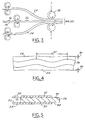
- FIG. 1 there is illustrated a schematic of cladding multiple sets 10, 12, 14 of tri-metals in one or more cladding rolls 16, 18, 20 and then combining all of the sets in a rolling mill 22.
- the first set of tri-metal 10 is illustrated as being driven through a first pair of cladding rollers 16.
- the three sheets, a pair of outside or second metal layers 24 and a central or first metal layer 26 of the metals, are shown enlarged for the purposes of illustration.
- Aluminum is the central layer 26 and a pair of sheets or outside layer 24 of copper is cladded to both broadside surfaces of the aluminum.
- each pair of cladding rollers 16, 18, 20, each pair forming a cladding mill there are three pairs of cladding rollers 16, 18, 20, each pair forming a cladding mill, as illustrated in Figure 1. It is understood that the number of pairs of cladding rollers comprising a cladding mill is at the option of the fabricator.
- the cladding process applies a heavy pressure to the tri-metal 10 and causes a bonding of the three metals.
- Each of the sheets 24, 26 of metal is smooth prior to being fed into the cladding rollers 16, 18, 20.
- the heavy pressure of the cladding rollers not only reduces the thickness of the tri-metal set, but also introduces more waviness into the middle layer of the tri-metal. It is for this reason that the cladding rollers are of a very large diameter so as to have a large surface contact with the tri-metal set thereby reducing the waviness.
- the top and bottom surface 24 of the tri-metal set as previously indicated is copper.
- the outside layers of the copper are oxidized to prevent bonding between the sets 10, 12, 14 in the rolling mill 22 thereby allowing an increase in the throughput of the cladding mills.
- the initial material stock is closer to the desired finish tolerances of the ETM sheet construction.
- the stresses in the material that are normally introduced by the cladding process are reduced.
- the method of Figure 1 comprises the steps of first forming a stacked set of tri-metal material 10, 12, 14 having three layers of metal wherein the central layer 26 is one material and the top and bottom layers 24 are a second material.
- the oxidizing layer is a copper oxidizing layer that will not adhere to the outside layer of another individual set of tri-metal materials.
- each individual set of the tri-metal material is fed to a cladding mill 16, 18, 20 or roller to form a tri-metal cladded material.
- a cladding mill 16 or roller As each set of the tri-metal material leaves the cladding mill, they are positioned in an overlying manner on another set so that the oxidizing surfaces are adjacent to each other to create a multiple set of tri-metal cladded material sets.
- the multiple sets are then supplied to a rolling mill 22 at a predetermined pressure and temperature for reducing the thickness of the multiple set of tri-metal cladded material.
- each individual set 10, 12, 14 of tri-metal cladded material is then separated from each other.
- FIG. 2 there is illustrated another embodiment of forming a set of tri-metal cladded material.
- the individual sheets 24, 26 are supplied via rollers 28 to the clad mill 30.
- a removable layer 32 on the outside surface of both the top and bottom layer 24 is a removable layer 32.
- the tri-metal material 10 is formed of copper on the outside and aluminum in the middle.
- the method illustrated in Figure 2 for cladding material for etched-tri-metal circuits to maintain the dimensional tolerance and reducing the stresses in the cladded material has the steps of individually rolling three layers 24, 26, 24 of metal wherein a central layer 26 is one material, such as aluminum, and the top and bottom layers 24 are a second material, such as copper, forming a tri-metal material 10.
- a removable layer 32 such as tungsten, is added on the outside surface of the top and bottom layer 24 .
- the tri-metal material 10 with the two removable layers 32 forms a set of five-layer material 34 with the removable layers on the outside,
- the set of five-layer material 34 is supplied to a cladding mill 30 to clad the material at a predetermined pressure and temperature for cladding of the tri-metal material 10.
- the set of five-layer material 34 is rolled at a predetermined pressure and temperature to a predetermined thickness and then the removable layers 32 are removed resulting in a tri-metal cladded material 10.
- FIG. 3 Another embodiment is illustrated in Figure 3.
- the outer broadside surfaces of the central material 26 are coated with a thin layer 36 of a bonding metal such as silver or tin or an aluminum alloy before the material is supplied to the cladding mill 38.
- the outer layers 24 are placed on the bonding layer 36 for bonding to the central layer 26.
- the inside surfaces of the outer layers 24 may have the bonding material layer applied thereto.
- the tri-metal material set is then supplied to the cladding mill 38 to complete the bonding and to reduce the thickness of the layers.
- This bonding material reduces or eliminates a brittle Cu/Al intermetallic formation. Thick Cu/Al intermetallics at the interface make the copper and aluminum layers debond after cladding.
- the thickness of the bonding layer 36 is on the order of microns and typically is less than three microns.
- bonding metal layers that can be used to enhance the copper-aluminum bonding and to prevent or reduce intermetallic formation include tin, nickel, titanium, chromium, aluminum and zinc and any of their alloys. Any of these metals, including silver, can be deposited by any of the standard deposition techniques such as plating, cladding, sputtering, etc. These bonding metals amalgamate into the aluminum and are not recoverable.
- Figure 4 illustrates the washboard effect with unacceptable variations in thickness of the copper and aluminum currently available.
- the waviness of the outside surface 40 may be 0.0015 inches (0.0381 mm)
- the thickness of the copper layer 26 between 0.002 inches (0.580 mm) and 0.0035 inches (0.889 mm)
- the peak to peak dimension 42 may be 0.100 inches (25.4 mm).
- An example of the material used in the method of Figures 1-3 is 3003 aluminum and 110 copper.
- an etched-tri-metal sheet 44 having a central first metal layer 26 of aluminum having two broadside surfaces 46, 48.
- a pair of second metal layers 24 of copper each having two broadside surfaces 50-53 that are substantially identical in shape to the broadside surfaces 46, 48 of the first metal layer 26 overlie each of the broadside surfaces of the central layer forming a sandwich.
- a bonding material is interposed the broadside surfaces 46, 51 and 48, 52, of the first 26 and second 24 metal layers.
- the bonding material is coated on the broadside surfaces of the central metal layer 26.
- a removable layer 32 is positioned on the top 50 and bottom 53 outside broadside surface of the second metal layers 24. This removable layer 32 is fabricated from tin, tungsten forming a five-layer sheet 34.
- the bonding material is selected from a group consisting of tin, nickel, titanium, chromium, silver and zinc.
- the outside broadside surfaces 50, 53 of the copper is covered with a copper oxide for preventing stacked tri-metal sheet sets 10, 12, 14 from adhering to each other.
Landscapes
- Engineering & Computer Science (AREA)
- Manufacturing & Machinery (AREA)
- Microelectronics & Electronic Packaging (AREA)
- Pressure Welding/Diffusion-Bonding (AREA)
- Laminated Bodies (AREA)
- Production Of Multi-Layered Print Wiring Board (AREA)
- Metal Rolling (AREA)
- Parts Printed On Printed Circuit Boards (AREA)
Abstract
Description
Claims (5)
- A method for cladding material for etched-tri-metal circuits to maintain the dimensional tolerance and reducing the stresses in the cladded material, the method comprising:forming a stacked set of tri-metal material having three layers of metal wherein the central layer is one material and the top and bottom layers are a second material;oxidizing the outside surface of the top and bottom layers of each set of tri-metal material;individually cladding a plurality of sets of the tri-metal material forming a tri-metal cladded material;overlying each set tri-metal cladded material on another set so that the oxidizing surfaces are adjacent to each other to create a multiple set of tri-metal cladded material sets; androlling the multiple set of tri-metal cladded material sets at a predetermined pressure and temperature for reducing the thickness of the multiple set of tri-metal cladded material.
- The method according to claim 1 wherein the central layer is aluminum.
- The method according to claim 1 wherein the top and bottom layers are copper.
- The method according to claim 1 wherein the oxidizing surface is a copper oxidizing layer that will not adhere to either the top or bottom layer.
- The method according to claim 1 additionally including the step of separating after the step of rolling each of the tri-metal cladded material sets from each other.
Applications Claiming Priority (2)
| Application Number | Priority Date | Filing Date | Title |
|---|---|---|---|
| US09/703,553 US6454878B1 (en) | 2000-11-01 | 2000-11-01 | Cladded material construction for etched-tri-metal circuits |
| US703553 | 2000-11-01 |
Publications (3)
| Publication Number | Publication Date |
|---|---|
| EP1204303A2 true EP1204303A2 (en) | 2002-05-08 |
| EP1204303A3 EP1204303A3 (en) | 2002-12-11 |
| EP1204303B1 EP1204303B1 (en) | 2003-09-17 |
Family
ID=24825838
Family Applications (1)
| Application Number | Title | Priority Date | Filing Date |
|---|---|---|---|
| EP01125894A Expired - Lifetime EP1204303B1 (en) | 2000-11-01 | 2001-10-30 | Cladded material construction for etched-tri-metal circuits |
Country Status (4)
| Country | Link |
|---|---|
| US (1) | US6454878B1 (en) |
| EP (1) | EP1204303B1 (en) |
| JP (1) | JP2002232096A (en) |
| DE (1) | DE60100780T2 (en) |
Cited By (4)
| Publication number | Priority date | Publication date | Assignee | Title |
|---|---|---|---|---|
| EP1342564A4 (en) * | 2000-10-18 | 2010-03-03 | Toyo Kohan Co Ltd | Multilayered metal laminate and process for producing the same |
| CN107755878A (en) * | 2016-08-23 | 2018-03-06 | 张颖 | A kind of method for preparing metallic laminate |
| CN113020924A (en) * | 2021-02-26 | 2021-06-25 | 醴陵千汇实业有限公司 | Production method for improving durability of rolling type die |
| EP4566732A4 (en) * | 2022-08-02 | 2025-12-03 | Proterial Ltd | CLATED MATERIAL AND METHOD FOR PRODUCING CLATED MATERIAL |
Families Citing this family (6)
| Publication number | Priority date | Publication date | Assignee | Title |
|---|---|---|---|---|
| US7293355B2 (en) * | 2005-04-21 | 2007-11-13 | Endicott Interconnect Technologies, Inc. | Apparatus and method for making circuitized substrates in a continuous manner |
| JP5730089B2 (en) * | 2011-03-23 | 2015-06-03 | 日本発條株式会社 | Conductive material, laminate, and method for producing conductive material |
| CN103394510A (en) * | 2013-07-31 | 2013-11-20 | 山东莱芜金石集团有限公司 | Cold-rolled copper and aluminum composite material production process |
| WO2019176937A1 (en) * | 2018-03-14 | 2019-09-19 | 東洋鋼鈑株式会社 | Roll-bonded body and production method for same |
| JP7085419B2 (en) * | 2018-03-14 | 2022-06-16 | 東洋鋼鈑株式会社 | Rolled joint and its manufacturing method |
| CN113102503B (en) * | 2021-04-15 | 2022-02-08 | 西安艾蒙希科技有限公司 | Preparation method of titanium-aluminum composite ultrathin plate with sandwich structure |
Family Cites Families (10)
| Publication number | Priority date | Publication date | Assignee | Title |
|---|---|---|---|---|
| JPS5146904B2 (en) | 1971-09-30 | 1976-12-11 | ||
| JPS5545382B2 (en) * | 1972-10-04 | 1980-11-18 | ||
| DE3106607C2 (en) * | 1981-02-23 | 1987-08-20 | Fr. Kammerer GmbH, 7530 Pforzheim | Plating process |
| US4404059A (en) | 1982-05-26 | 1983-09-13 | Livshits Vladimir I | Process for manufacturing panels to be used in microelectronic systems |
| US4659425A (en) * | 1986-02-03 | 1987-04-21 | Ibm Corporation | Continuous process for the manufacture of printed circuit boards |
| SE9203327L (en) * | 1992-11-06 | 1993-12-20 | Metfoils Ab | Process for the production of printed circuit boards and their use |
| JPH0910965A (en) * | 1995-06-30 | 1997-01-14 | Japan Steel Works Ltd:The | Separation agent for clad steel and method for manufacturing clad steel sheet |
| US5738797A (en) | 1996-05-17 | 1998-04-14 | Ford Global Technologies, Inc. | Three-dimensional multi-layer circuit structure and method for forming the same |
| US5976391A (en) * | 1998-01-13 | 1999-11-02 | Ford Motor Company | Continuous Flexible chemically-milled circuit assembly with multiple conductor layers and method of making same |
| US6217783B1 (en) * | 1998-12-01 | 2001-04-17 | Visteon Global Technologies, Inc. | Method for strengthening air bridge circuits |
-
2000
- 2000-11-01 US US09/703,553 patent/US6454878B1/en not_active Expired - Fee Related
-
2001
- 2001-10-30 EP EP01125894A patent/EP1204303B1/en not_active Expired - Lifetime
- 2001-10-30 DE DE60100780T patent/DE60100780T2/en not_active Expired - Fee Related
- 2001-11-01 JP JP2001336706A patent/JP2002232096A/en not_active Ceased
Cited By (5)
| Publication number | Priority date | Publication date | Assignee | Title |
|---|---|---|---|---|
| EP1342564A4 (en) * | 2000-10-18 | 2010-03-03 | Toyo Kohan Co Ltd | Multilayered metal laminate and process for producing the same |
| CN107755878A (en) * | 2016-08-23 | 2018-03-06 | 张颖 | A kind of method for preparing metallic laminate |
| CN107755878B (en) * | 2016-08-23 | 2021-09-03 | 张颖 | Method for preparing metal laminated material |
| CN113020924A (en) * | 2021-02-26 | 2021-06-25 | 醴陵千汇实业有限公司 | Production method for improving durability of rolling type die |
| EP4566732A4 (en) * | 2022-08-02 | 2025-12-03 | Proterial Ltd | CLATED MATERIAL AND METHOD FOR PRODUCING CLATED MATERIAL |
Also Published As
| Publication number | Publication date |
|---|---|
| EP1204303B1 (en) | 2003-09-17 |
| DE60100780D1 (en) | 2003-10-23 |
| EP1204303A3 (en) | 2002-12-11 |
| US6454878B1 (en) | 2002-09-24 |
| DE60100780T2 (en) | 2004-08-05 |
| JP2002232096A (en) | 2002-08-16 |
Similar Documents
| Publication | Publication Date | Title |
|---|---|---|
| DE60120454T2 (en) | FILM WITH MULTILAYER METAL AND METHOD FOR THE PRODUCTION THEREOF | |
| EP1204303B1 (en) | Cladded material construction for etched-tri-metal circuits | |
| US7175919B2 (en) | Multilayered metal laminate and process for producing the same | |
| EP1345728B1 (en) | Method of making a composite aluminium sheet | |
| EP2662176B1 (en) | Method for producing a metallic laminated multi-layer film, in particular a laminated multi-layer film in the form of a tape | |
| EP1581360B1 (en) | Method for the production of a strip comprising a staggered profile that runs in the longitudinal direction thereof | |
| EP0564151A2 (en) | Drum cathode for use in the production of metal foils and a method of producing the same | |
| US4452664A (en) | Method for predetermining peel strength at copper/aluminum interface | |
| EP1086776B1 (en) | Laminated ribbon and method and apparatus for producing same | |
| CN110303044B (en) | Control method for bonding pass rolling of aluminum composite plate roughing mill | |
| EP0996318B1 (en) | Novel composite foil, process for producing the same and copper-clad laminate | |
| JP4744938B2 (en) | Metal materials for printed wiring boards | |
| US6673471B2 (en) | Corrosion prevention for CAC component | |
| JP4677381B2 (en) | Metal materials for printed wiring boards | |
| RU2152858C1 (en) | Bimetallic composition and method of manufacture thereof | |
| JP4744937B2 (en) | Metal materials for printed wiring boards | |
| JPH0688145B2 (en) | Roll bonding method for clad plates | |
| TWI806296B (en) | Surface treated copper foil, copper clad laminate and printed wiring board | |
| JPH057903A (en) | Aluminum foil manufacturing method | |
| CN108480400A (en) | A kind of dissimilar metal mutually spells composite board band and preparation method thereof | |
| JPS6326398A (en) | Production of silicon steel sheet for printed circuit board | |
| SU870037A1 (en) | Method o producing multilayer metals and alloys | |
| CN121988609A (en) | Glue-coated rolled copper foil and manufacturing method thereof | |
| JPS6099493A (en) | Production of clad plate | |
| JPH03287795A (en) | Bright ni plated steel strip and production thereof |
Legal Events
| Date | Code | Title | Description |
|---|---|---|---|
| PUAI | Public reference made under article 153(3) epc to a published international application that has entered the european phase |
Free format text: ORIGINAL CODE: 0009012 |
|
| AK | Designated contracting states |
Kind code of ref document: A2 Designated state(s): AT BE CH CY DE DK ES FI FR GB GR IE IT LI LU MC NL PT SE TR |
|
| AX | Request for extension of the european patent |
Free format text: AL;LT;LV;MK;RO;SI |
|
| 17P | Request for examination filed |
Effective date: 20020613 |
|
| PUAL | Search report despatched |
Free format text: ORIGINAL CODE: 0009013 |
|
| RIC1 | Information provided on ipc code assigned before grant |
Free format text: 7H 05K 1/09 A, 7H 05K 3/02 B, 7B 23K 20/04 B |
|
| AK | Designated contracting states |
Kind code of ref document: A3 Designated state(s): AT BE CH CY DE DK ES FI FR GB GR IE IT LI LU MC NL PT SE TR |
|
| AX | Request for extension of the european patent |
Free format text: AL;LT;LV;MK;RO;SI |
|
| GRAH | Despatch of communication of intention to grant a patent |
Free format text: ORIGINAL CODE: EPIDOS IGRA |
|
| GRAS | Grant fee paid |
Free format text: ORIGINAL CODE: EPIDOSNIGR3 |
|
| GRAA | (expected) grant |
Free format text: ORIGINAL CODE: 0009210 |
|
| AKX | Designation fees paid |
Designated state(s): DE FR GB |
|
| AK | Designated contracting states |
Kind code of ref document: B1 Designated state(s): DE FR GB |
|
| REG | Reference to a national code |
Ref country code: GB Ref legal event code: FG4D |
|
| PGFP | Annual fee paid to national office [announced via postgrant information from national office to epo] |
Ref country code: FR Payment date: 20031009 Year of fee payment: 3 |
|
| REF | Corresponds to: |
Ref document number: 60100780 Country of ref document: DE Date of ref document: 20031023 Kind code of ref document: P |
|
| REG | Reference to a national code |
Ref country code: IE Ref legal event code: FG4D |
|
| PG25 | Lapsed in a contracting state [announced via postgrant information from national office to epo] |
Ref country code: DE Free format text: LAPSE BECAUSE OF NON-PAYMENT OF DUE FEES Effective date: 20040501 |
|
| ET | Fr: translation filed | ||
| PLBE | No opposition filed within time limit |
Free format text: ORIGINAL CODE: 0009261 |
|
| STAA | Information on the status of an ep patent application or granted ep patent |
Free format text: STATUS: NO OPPOSITION FILED WITHIN TIME LIMIT |
|
| REG | Reference to a national code |
Ref country code: IE Ref legal event code: MM4A |
|
| 26N | No opposition filed |
Effective date: 20040618 |
|
| PG25 | Lapsed in a contracting state [announced via postgrant information from national office to epo] |
Ref country code: FR Free format text: LAPSE BECAUSE OF NON-PAYMENT OF DUE FEES Effective date: 20050630 |
|
| REG | Reference to a national code |
Ref country code: FR Ref legal event code: ST |
|
| PG25 | Lapsed in a contracting state [announced via postgrant information from national office to epo] |
Ref country code: GB Free format text: LAPSE BECAUSE OF NON-PAYMENT OF DUE FEES Effective date: 20051030 |
|
| GBPC | Gb: european patent ceased through non-payment of renewal fee |
Effective date: 20051030 |