EP1202351A2 - Protection circuit provided in semiconductor circuit - Google Patents
Protection circuit provided in semiconductor circuit Download PDFInfo
- Publication number
- EP1202351A2 EP1202351A2 EP01124383A EP01124383A EP1202351A2 EP 1202351 A2 EP1202351 A2 EP 1202351A2 EP 01124383 A EP01124383 A EP 01124383A EP 01124383 A EP01124383 A EP 01124383A EP 1202351 A2 EP1202351 A2 EP 1202351A2
- Authority
- EP
- European Patent Office
- Prior art keywords
- gate
- drain
- mos transistor
- source
- power supply
- Prior art date
- Legal status (The legal status is an assumption and is not a legal conclusion. Google has not performed a legal analysis and makes no representation as to the accuracy of the status listed.)
- Withdrawn
Links
Images



Classifications
-
- H—ELECTRICITY
- H10—SEMICONDUCTOR DEVICES; ELECTRIC SOLID-STATE DEVICES NOT OTHERWISE PROVIDED FOR
- H10D—INORGANIC ELECTRIC SEMICONDUCTOR DEVICES
- H10D84/00—Integrated devices formed in or on semiconductor substrates that comprise only semiconducting layers, e.g. on Si wafers or on GaAs-on-Si wafers
-
- H—ELECTRICITY
- H10—SEMICONDUCTOR DEVICES; ELECTRIC SOLID-STATE DEVICES NOT OTHERWISE PROVIDED FOR
- H10D—INORGANIC ELECTRIC SEMICONDUCTOR DEVICES
- H10D89/00—Aspects of integrated devices not covered by groups H10D84/00 - H10D88/00
- H10D89/60—Integrated devices comprising arrangements for electrical or thermal protection, e.g. protection circuits against electrostatic discharge [ESD]
- H10D89/601—Integrated devices comprising arrangements for electrical or thermal protection, e.g. protection circuits against electrostatic discharge [ESD] for devices having insulated gate electrodes, e.g. for IGFETs or IGBTs
- H10D89/811—Integrated devices comprising arrangements for electrical or thermal protection, e.g. protection circuits against electrostatic discharge [ESD] for devices having insulated gate electrodes, e.g. for IGFETs or IGBTs using FETs as protective elements
Definitions
- This invention relates to a protection circuit provided in a semiconductor circuit, and more particularly, to a protection circuit for protecting a semiconductor circuit from being broken by static electricity.
- a protection circuit formed of MOS elements is arranged between a power supply terminal and a ground terminal for conducting a charge generated by static electricity, which has introduced into the power supply terminal, to the ground terminal.
- the conventional protection circuit will be described below with reference to FIGS. 1A to 1C.
- FIG. 1A is a circuit diagram illustrating the configuration of the conventional protection circuit
- FIG. 1B is a schematic cross-sectional view of the protection circuit
- FIG. 1C illustrates a layout of the protection circuit on a semiconductor substrate.
- this protection circuit comprises a p-channel MOS transistor (hereinafter denoted "p-MOS transistor”) P11, and an n-channel MOS transistor (hereinafter denoted "n-MOS transistor”) N11.
- p-MOS transistor p-channel MOS transistor
- n-MOS transistor n-channel MOS transistor
- the p-MOS transistor P11 has a source, a gate and a back gate connected to a power supply terminal TV which is supplied with a power supply potential Vcc.
- the n-MOS transistor N11 has a drain connected to a power supply terminal TV, and a source, a gate and a back gate connected to a ground terminal TG supplied with a ground potential GND. Further, the p-MOS transistor P11 has a drain connected to the ground terminal TG.
- FIG. 1B A general structure of the protection circuit in cross-section is as illustrated in FIG. 1B.
- An n-type well 102 is formed within a p-type silicon semiconductor substrate 101, and an element region separated by an element separation insulating film 103 is formed in the n-type well 102.
- a source region (p + -type) 104 and a drain region (p + -type) 105 are formed in the n-type well 102 of the element region.
- a gate electrode 107 is placed on a channel between the source region 104 and the drain region 105, with a gate insulating film (not shown) therebetween.
- the p-MOS transistor P11 is formed of these components.
- a source region (n + -type) 121 and a drain region (n + -type) 122 are formed within the p-type semiconductor substrate 101.
- a gate electrode 124 is placed on a channel between the source region 121 and the drain region 122, with a gate insulating film (not shown) therebetween.
- the n-MOS transistor N11 is formed of these components.
- the power supply terminal TV is connected to the source region 104, gate electrode 107 and n-type well 102 of the p-MOS transistor P11.
- the n-MOS transistor N11 has the drain region 122 connected to the power supply terminal TV, and the source region 121, gate electrode 124 and p-type semiconductor substrate 101 connected to the ground terminal TG. Also, the p-MOS transistor P11 has the drain region 105 connected to the ground terminal TG.
- the protection circuit is laid out on the semiconductor substrate as illustrated in FIG. 1C.
- the source region 104 and drain region 105 which comprise the p-MOS transistor P11, are separately positioned.
- the gate electrode 107 is arranged between the source region 104 and drain region 105.
- a source contact 104A is placed in the source region 104, while a drain contact 105A is placed in the drain region 105.
- the distance between the drain contact 105A and gate electrode 107 is longer than the distance between the source contact 104A and gate electrode 107.
- the source region 121 and drain region 122 which comprise the n-MOS transistor N11, are separately positioned.
- the gate electrode 124 is arranged between the source region 121 and drain region 122.
- a source contact 121A is placed in the source region 121, while a drain contact 122A is placed in the drain region 122.
- the distance between the drain contact 122A and gate electrode 124 is longer than the distance between the source contact 121A and gate electrode 124.
- An object of the present invention which has been achieved in view of the situation described above, is to provide a protection circuit which is capable of improving the tolerance of a semiconductor circuit to static electricity.
- a protection circuit comprises a power supply terminal supplied with a power supply potential, a reference terminal supplied with a reference potential, a first p-channel MOS transistor having a gate, a source, a drain and a back gate, wherein the gate, the source and the back gate are connected to the power supply terminal, a second p-channel MOS transistor having a gate, a source, a drain and a back gate, wherein the source is connected to the drain of the first p-channel MOS transistor, the back gate is connected to the power supply terminal, and the gate and the drain are connected to the reference terminal, a first n-channel MOS transistor having a gate, a source, a drain and a back gate, wherein the gate, the source and the back gate are connected to the reference terminal, and a second n-channel MOS transistor having a gate, a source, a drain and a back gate, wherein the source is connected to the drain of the first n-channel NOS transistor,
- p-MOS transistor p-channel MOS transistors
- n-MOS transistor n-channel MOS transistors
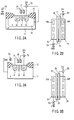
- FIG. 2A is a schematic cross-sectional view of the p-channel MOS transistors which form part of the protection circuit according to the first embodiment.
- FIG. 2B illustrates a layout of the p-channel MOS transistors on a semiconductor substrate.
- an n-type well 12 is formed within a p-type silicon semiconductor substrate 11, and an element region is formed in the n-type well 12 and separated by an element separation insulating film 13.
- an element region is formed in the n-type well 12 and separated by an element separation insulating film 13.
- Formed within the n-type well 12 of this element region are a source region (p + -type) 14 and a drain region (p + -type) 15 spaced apart by a predetermined distance.
- An island region (p + -type) 16 separated from these source region 14 and drain region 15 is formed between the source region 14 and drain region 15.
- a gate electrode 17 is formed on a channel between the source region 14 and island region 16, with a gate insulating film (not shown) therebetween.
- a gate electrode 18 is formed on a channel between the island region 16 and drain region 15, with a gate insulating film (not shown) therebetween.
- a p-MOS transistor P1 is formed of the foregoing source region 14, island region 16, channel between these source region 14 and island region 16, and gate electrode 17 on the channel. Also, a p-MOS transistor P2 is formed of the island region 16, drain region 15, channel between these island region 16 and drain region 15, and gate electrode 18 on the channel.
- a power supply terminal TV supplied with a power supply potential Vcc, is connected to the source region 14, gate electrode 17 and n-type well 12 of the p-MOS transistor P1.
- a ground terminal (or a reference terminal) TG supplied with a ground potential GND (or a reference potential), is connected to the drain region 15 and gate electrode 18 of the p-MOS transistor P2.
- the p-channel MOS transistors P1, P2 are laid out on a semiconductor substrate as illustrated in FIG. 2B.
- the source region 14, island region 16 and drain region 15, comprising the p-MOS transistors P1, P2, are positioned separately from one another.
- the gate electrode 17 is positioned between the source region 14 and island region 16, while the gate electrode 18 is positioned between the island region 16 and drain region 15.
- a source contact 14A is placed in the source region 14 for connecting the source region 14 to a wiring layer (not shown).
- a drain contact 15A is placed in the drain region 15 for connecting the drain region 15 to a wiring layer (not shown).
- the distance between the drain contact 15A and gate electrode 18 is longer than the distance between the source contact 14A and gate electrode 17 which are placed in conformity to a design rule.
- the p-channel MOS transistors P1, P2 include an additional wiring layer (gate electrode 18) on the gate insulating film between the source and drain (defined as a gate region), connected to the ground terminal TG, as added to the p-channel MOS transistor P11 which forms part of the conventional protection circuit. Therefore, the area occupied by the source region 14, island region 16, drain region 15 and channels of the p-MOS transistors P1, P2 is as wide as the area occupied by the source region 104, drain region 105 and channel of the conventional p-MOS transistor P11, without requiring a larger area, as compared with the conventional p-MOS transistor P11, for forming the p-MOS transistors P1, P2.
- the gate electrode 18 is excited to the minus potential to form a channel in a portion of the gate region between the source region 14 and the drain region 15, so that the apparent transistor channel length becomes shorter than that of the conventional protection element (the p-MOS transistor P11).
- FIG. 3A is a schematic cross-sectional view of the n-channel MOS transistors which comprise the protection circuit according to the first embodiment.
- FIG. 3B illustrates a layout of the n-channel MOS transistors on a semiconductor substrate.
- an element region As illustrated in FIG. 3A, an element region, separated by an element separation insulating film 13, is formed within a p-type silicon semiconductor substrate 11.
- a source region (n + -type) 21 and a drain region (n + -type) 22 are formed spaced apart by a predetermined distance within the p-type substrate 11 in the element region.
- a gate electrode 24 is formed on a channel between the source region 21 and island region 23, with a gate insulating film (not shown) therebetween.
- a gate electrode 25 is formed on a channel between the island region 23 and drain region 22, with a gate insulating film (not shown) therebetween.
- n-MOS transistor N1 is formed of the foregoing source region 21, island region 23, channel between the source region 21 and island region 23, and gate electrode 24 on the channel. Also, an n-MOS transistor N2 is formed of the island region 23, drain region 22, channel between the island region 23 and drain region 22, and gate electrode 25 on the channel.
- the ground terminal TG supplied with the ground potential, is connected to the source region 21, gate electrode 24 and p-type substrate 11 of the n-MOS transistor N1.
- the power supply terminal TV supplied with the power supply potential Vcc, is connected to the drain region 22 and gate electrode 25 of the n-MOS transistor N2.
- the n-channel MOS transistors N1, N2 are laid out on the semiconductor substrate as illustrated in FIG. 3B.
- the source region 21, island region 23, and drain region 22, comprising the n-MOS transistors N1, N2, are positioned separately from one another.
- the gate electrode 24 is positioned between the source region 21 and island region 23, while the gate electrode 25 is positioned between the island region 23 and drain region 22.
- a source contact 21A is placed in the source region 21 for connecting the source region 21 to a wiring layer (not shown).
- a drain contact 22A is placed in the drain region 22 for connecting the drain region 22 to a wiring layer (not shown).
- the distance between the drain contact 22A and gate electrode 25 is longer than the distance between the source contact 21A and gate electrode 24 which are positioned in conformity to the design rule.
- the n-channel MOS transistors N1, N2 include the additional wiring layer (gate electrode 25) connected to the power supply terminal TV on the gate insulating film between the source and drain (defined as the gate region), as added to the n-channel MOS transistor N11 which forms part of the conventional protection circuit. Therefore, the area occupied by the source region 21, island region 23, drain region 22, and channels of the n-MOS transistors N1, N2 is as wide as the area occupied by the source region 121, drain region 122, and channel of the conventional n-MOS transistor N11, without requiring a larger area, as compared with the conventional n-MOS transistor N11, for forming the n-MOS transistors N1, N2.
- n-channel MOS transistors N1, N2 formed in the foregoing manner, under the condition that the ground terminal TG is connected to the ground potential GND with the power supply terminal TV being left in floating state, when static electricity having a plus potential, applied to the input terminal or output terminal, introduces into the gate electrode 25 in floating state, the gate electrode 25 is excited to the plus potential to form a channel in a portion of the gate region between the source region 21 and the drain region 22, so that the apparent transistor channel length becomes shorter than that of the conventional protection element (the n-MOS transistor N11).
- the charge which has introduced into the power supply terminal TV by the application of the static electricity having the plus potential, can be readily led to the ground potential GND through the ground terminal TG, thereby making it possible to obviate the internal elements from being broken by the static electricity.
- the protection circuit according to the first embodiment which comprises the p-channel MOS transistors P1, P2 and n-channel MOS transistors N1, N2.
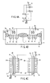
- FIG. 4A is a circuit diagram illustrating the protection circuit according to the first embodiment
- FIG. 4B is a schematic cross-sectional view of the protection circuit
- FIG. 4C illustrates a layout of the protection circuit on a semiconductor substrate.
- this protection circuit comprises the p-channel MOS transistors P1, P2, and n-channel MOS transistors N1, N2.
- the p-channel MOS transistor P1 has the source, gate, and back gate connected to the power supply terminal TV which is supplied with the power supply potential Vcc.
- the p-MOS transistor P1 has the drain connected to the source of the p-MOS transistor P2.
- the p-MOS transistor P2 has a back gate connected to the power supply terminal TV, and the drain and gate connected to the ground terminal TG which is supplied with the ground potential GND.
- the n-MOS transistor N1 has the source, gate and back gate connected to the ground terminal TG.
- the n-MOS transistor N1 has the drain connected to the source of the n-MOS transistor N2.
- the n-MOS transistor N2 has the drain and gate connected to the power supply terminal TV, and its back gate connected to the ground terminal TG.
- the general structure of the protection circuit in cross-section includes the p-MOS transistors P1, P2 illustrated in FIG. 2 and the n-MOS transistors N1, N2 illustrated in FIG. 3A, which are positioned adjacent to each other, with the power supply terminal TV and ground terminal TG used common to them.
- the layout of the protection circuit on the semiconductor substrate, as illustrated in FIG. 4C, includes the p-MOS transistors P1, P2 illustrated in FIG. 2B and the n-MOS transistors N1, N2 illustrated in FIG. 3B, which are positioned adjacent to each other, with the power supply terminal TV and ground terminal TG used common to them.
- the protection circuit according to the first embodiment is connected between a power supply line supplied with the power supply potential Vcc and a ground line supplied with the ground potential GND in the semiconductor circuit for use therewith.
- the protection circuit configured in the foregoing manner, with the power supply terminal TV connected to the power supply potential Vcc and the ground terminal TG left in floating state, when static electricity having a minus potential, applied to the input terminal or output terminal, introduces into the gate electrode 18 in floating state, the gate electrode 18 is excited to the minus potential to form a channel in a portion of the gate region between the source region 14 and the drain region 15, so that the apparent transistor channel length becomes shorter than that of the conventional protection element (the p-MOS transistor P11), as described above.
- the conventional protection element the p-MOS transistor P11
- FIGS. 2A, 2B Next described will be a first example in which the p-MOS transistors P1, P2 illustrated in FIGS. 2A, 2B are connected between the power supply terminal TV and an input/output terminal I/O; a second example in which the n-MOS transistors N1, N2 illustrated in FIGS. 3A, 3B are connected between the ground terminal TG and input/output terminal I/O; and a third example which is a combination of the first and second examples, as a protection circuit according to a second embodiment of this invention.
- FIG. 5 illustrates a layout on a semiconductor substrate, illustrating the configuration of a protection circuit (first example) according to the second embodiment.
- the p-MOS transistor P1 has the source region 14, gate electrode 17, and back gate (not shown), which is an n-type well, connected to the power supply terminal TV which is supplied with the power supply potential Vcc.
- the p-MOS transistor P2 has the drain region 15 and gate electrode 18 connected to the input/output terminal I/O through which an input signal or an output signal is input or output.
- the rest of the configuration is similar to the configuration illustrated in FIG. 2B.
- the protection circuit configured in the foregoing manner, with the power supply terminal TV connected to the power supply potential Vcc, when static electricity having a minus potential, applied to the input/output terminal I/O, introduces into the gate electrode 18, the gate electrode 18 is excited to the minus potential to form a channel in a portion of the gate region between the source region 14 and the drain region 15, so that the apparent transistor channel length becomes shorter than that of the conventional protection element (the p-MOS transistor P11).
- the charge which has introduced into the input/output terminal I/O by the application of the static electricity having the minus potential, can be readily led to the power supply potential Vcc through the power supply terminal TV, thereby making it possible to obviate the internal elements from being broken by the static electricity.
- FIG. 6 is a layout on a semiconductor substrate, illustrating the configuration of a protection circuit (second example) according to the second embodiment.
- the n-MOS transistor N1 has the source region 21, gate electrode 24 and back gate (not shown), which is the p-type substrate, connected to the ground terminal TG which is supplied with the ground potential.
- the n-MOS transistor N2 has the drain region 22 and gate electrode 25 connected to the input/output terminal I/O through which an input signal or an output signal is input or output.
- the rest of the configuration is similar to the configuration illustrated in FIG. 3B.
- the protection circuit configured in the foregoing manner, with the ground terminal TG connected to the ground potential GND, when static electricity having a plus potential, applied to the input/output terminal I/O, introduces into the gate electrode 25, the gate electrode 25 is excited to the plus potential to form a channel in a portion of the gate region between the source region 21 and the drain region 22, so that the apparent transistor channel length becomes shorter than that of the conventional protection element (the n-MOS transistor N11).
- the charge which has introduced into the input/output terminal I/O by the application of the static electricity having the plus potential, can be readily led to the ground potential GND through the ground terminal TG, thereby making it possible to obviate the internal elements from being broken by the static electricity.
- FIG. 7A is a circuit diagram illustrating a protection circuit (third example) according to the second embodiment
- FIG. 7B is a schematic cross-sectional view of the protection circuit
- FIG. 7C illustrates a layout of the protection circuit on the semiconductor substrate.
- the protection circuit comprises the p-channel MOS transistors P1, P2 and n-channel MOS transistors N1, N2.
- the p-MOS transistor P1 has the source, gate, and back gate connected to the power supply terminal TV which is supplied with the power supply potential Vcc.
- the p-MOS transistor P1 has the drain connected to the source of the p-MOS transistor P2.
- the p-MOS transistor P2 has the back gate connected to the power supply terminal TV, and the drain and gate connected to the input/output terminal I/O through which an input signal or an output signal is input or output.
- the n-MOS transistor N1 has the source, gate, and back gate connected to the ground terminal TG which is supplied with the ground potential GND.
- the n-MOS transistor N1 has the drain connected to the source of the n-MOS transistor N2.
- the n-MOS transistor N2 has the drain and gate connected to the input/output terminal I/O, and the back gate connected to the ground terminal TG.
- the general structure of the protection circuit in cross-section includes the p-MOS transistors P1, P2 illustrated in FIG. 2A and the n-MOS transistors N1, N2 illustrated in FIG. 3A, which are positioned adjacent to each other. These transistors are connected to the power supply terminal TV, ground terminal TG, and input/output terminal I/O in the following manner.
- the p-MOS transistor P1 has the source region 14, gate electrode 17, and n-type well 12 connected to the power supply terminal TV which is supplied with the power supply potential Vcc.
- the p-MOS transistor P2 has the drain region 15 and gate electrode 18 connected to the input/output terminal I/O through which an input signal or an output signal is input or output.
- the n-MOS transistor N1 has the source region 21, gate electrode 24, and n-type substrate 11 connected to the ground terminal TG which is supplied with the ground potential GND.
- the n-MOS transistor N2 has the drain region 22 and gate electrode 25 connected to the input/output terminal I/O.
- the protection circuit is laid out on the semiconductor substrate such that the p-MOS transistors P1, P2 illustrated in FIG. 2B are positioned adjacent to the n-MOS transistors N1, N2 illustrated in FIG. 3B. These transistors are connected to the power supply terminal TV, ground terminal TG, and input/output terminal I/O in the manner described in connection with the structure illustrated in the cross-sectional view of FIG. 7B.
- the protection circuit configured in the foregoing manner, with the power supply terminal TV connected to the power supply potential Vcc and the ground terminal TG connected to the ground potential GND, when static electricity having a minus potential, applied to the input/output terminal I/O, introduces into the gate electrode 18, the gate electrode 18 is excited to the minus potential to form a channel in a portion of the gate region between the source region 14 and the drain region 15, so that the apparent transistor channel length becomes shorter than that of the conventional protection element (the p-MOS transistor P11).
- the charge which has introduced into the input/output terminal I/O by the application of the static electricity having the minus potential, can be readily led to the power supply potential Vcc through the power supply terminal TV, thereby making it possible to obviate the internal elements from being broken by the static electricity.
- FIG. 8 illustrates a layout on a semiconductor substrate, illustrating the configuration of a protection circuit (first example) according to the third embodiment.
- the p-MOS transistor P1 has the source region 14, gate electrode 17, and pack gate (not shown), which is an n-type well, connected to the power supply terminal TV supplied with the power supply potential Vcc.
- the p-MOS transistor P2 has the gate electrode 18 connected to the ground terminal TG which is supplied with the ground potential GND.
- the p-MOS transistor P2 has the drain region 15 connected to the input/output terminal I/O for inputting an input signal or outputting an output signal.
- the rest of the configuration is similar to the configuration illustrated in FIG. 2B.
- the gate electrode 18 is excited to the minus potential to form a channel in a portion of the gate region between the source region 14 and the drain region 15, so that the apparent transistor channel length becomes shorter than that of the conventional protection element (the p-MOS transistor P11).
- FIG. 9 is a layout on the semiconductor substrate illustrating the configuration of a protection circuit (second example) according to the third embodiment.
- the n-MOS transistor N1 has the source region 21, gate electrode 24 and back gate (not shown), which is the p-type substrate, connected to the ground terminal TG which is supplied with the ground potential.
- the n-MOS transistor N2 has the gate electrode 25 connected to the power supply terminal TV supplied with the power supply potential Vcc.
- the n-MOS transistor N2 has the drain region 22 connected to the input/ output terminal I/O through which an input signal or an output signal is input or output. The rest of the configuration is similar to the configuration illustrated in FIG. 3B.
- n-channel MOS transistors N1, N2 formed in the foregoing manner, under the condition that the ground terminal TG is connected to the ground potential GND with the power supply terminal TV being left in floating state, when static electricity having a plus potential, applied to the input terminal or output terminal, introduces into the gate electrode 25 in floating state, the gate electrode 25 is excited to the plus potential to form a channel in a portion of the gate region between the source region 21 and the drain region 22, so that the apparent transistor channel length becomes shorter than that of the conventional protection element (the n-MOS transistor N11).
- the charge which has introduced into the power supply terminal TV by the application of the static electricity having the plus potential, can be readily led to the ground potential GND through the ground terminal TG, thereby making it possible to obviate the internal elements from being broken by the static electricity.
- FIG. 10A is a circuit diagram illustrating the configuration of a protection circuit (third example) according to the third embodiment
- FIG. 10B is a schematic cross-sectional view of the protection circuit
- FIG. 10C illustrates a layout of the protection circuit on the semiconductor substrate.
- this protection circuit comprises the p-channel MOS transistors P1, P2 and n-channel MOS transistors N1, N2.
- the p-MOS transistor P1 has the source, gate and back gate connected to the power supply terminal TV which is supplied with the power supply potential Vcc.
- the p-MOS transistor P1 has the drain connected to the source of the p-MOS transistor P2.
- the p-MOS transistor P2 has the back gate connected to the power supply potential TV, and the gate connected to the ground terminal TG which is supplied with the ground potential GND.
- the n-MOS transistor N1 has the source, gate and back gate connected to the ground terminal TG.
- the n-MOS transistor N1 has the drain connected to the source of the n-MOS transistor N2.
- the n-MOS transistor N2 has the gate connected to the power supply terminal TV, and the back gate connected to the ground terminal TG.
- the drain of the p-MOS transistor P2 and the drain of the n-MOS transistor N2 are connected to the input/output terminal I/O through which an input signal or an output signal are input or output.
- the general structure of the protection circuit in cross-section includes the p-MOS transistors P1, P2 illustrated in FIG. 2A and the n-MOS transistors N1, N2 illustrated in FIG. 3A, which are positioned adjacent to each other. These transistors are connected to the power supply terminal TV, ground terminal TG, and input/output terminal I/O in the following manner.
- the source region 14, gate electrode 17 and n-type well 12 of the p-MOS transistor P1, and the gate electrode 25 of the n-MOS transistor N2 are connected to the power supply terminal TV which is supplied with the power supply potential Vcc.
- the source region 21, gate electrode 24 and p-type substrate 11 of the n-MOS transistor N1, and the gate electrode 18 of the p-MOS transistor P2 are connected to the ground terminal TG which is supplied with the ground potential GND.
- the drain region 15 of the p-MOS transistor P2 and the drain region 22 of the n-MOS transistor N2 are connected to the input/output terminal I/O through which an input signal or an output signal is input or output.
- the protection circuit is laid out on the semiconductor substrate such that the p-MOS transistors P1, P2 illustrated in FIG. 2B are positioned adjacent to the n-MOS transistors N1, N2 illustrated in FIG. 3B. These transistors are connected to the power supply terminal TV, ground terminal TG, and input/output terminal I/O in the manner as described in connection with the structure illustrated in the cross-sectional view of FIG. 10B.
- the gate electrode 18 is excited to the minus potential to form a channel in a portion of the gate region between the source region 14 and the drain region 15, so that the apparent transistor channel length becomes shorter than that of the conventional protection element (the p-MOS transistor P11).
- n-channel MOS transistors N1, N2 formed in the foregoing manner, under the condition that the ground terminal TG is connected to the ground potential GND with the power supply terminal TV being left in floating state, when static electricity having a plus potential, applied to the input terminal or output terminal, introduces into the gate electrode 25 in floating state, the gate electrode 25 is excited to the plus potential to form a channel in a portion of the gate region between the source region 21 and the drain region 22, so that the apparent transistor channel length becomes shorter than that of the conventional protection element (the n-MOS transistor N11).
- the charge which has introduced into the power supply terminal TV by the application of the static electricity having the plus potential, can be readily led to the ground potential GND through the ground terminal TG, thereby making it possible to obviate the internal elements from being broken by the static electricity.
Landscapes
- Semiconductor Integrated Circuits (AREA)
- Metal-Oxide And Bipolar Metal-Oxide Semiconductor Integrated Circuits (AREA)
Abstract
Description
Claims (12)
- A protection circuit characterized by comprising:a power supply terminal (TV) supplied with a power supply potential;a reference terminal (TG) supplied with a reference potential;a first p-channel MOS transistor (P1) having a gate (17), a source (14), a drain (16) and a back gate (12), said gate, said source and said back gate being connected to said power supply terminal (TV);a second p-channel MOS transistor (P2) having a gate (18), a source (16), a drain (15) and a back gate (12), said source (16) being connected to the drain (16) of said first p-channel MOS transistor (P1), said back gate being connected to said power supply terminal (TV), said gate and said drain being connected to said reference terminal (TG);a first n-channel MOS transistor (N1) having a gate (24), a source (21), a drain (23) and a back gate (11), said gate, said source and said back gate being connected to said reference terminal (TG); anda second n-channel MOS transistor (N2) having a gate (25), a source (23), a drain (22) and a back gate (11), said source (23) being connected to the drain (23) of said first n-channel NOS transistor (N1), said back gate being connected to said reference terminal (TG), said gate and said drain being connected to said power supply terminal (TV).
- A protection circuit according to claim 1, characterized in that said protection circuit is provided for a semiconductor circuit formed on a semiconductor substrate, wherein said power supply terminal (TV) is connected to a power supply line which is supplied with a power supply potential within said semiconductor circuit, and said reference potential (TG) is connected to a ground line which is supplied with a ground potential within said semiconductor circuit.
- A protection circuit characterized by comprising:a power supply terminal (TV) supplied with a power supply potential;an input/output terminal (I/O) inputting and outputting a signal therethrough;a first p-channel NOS transistor (P1) having a gate (17), a source (14), a drain (16) and a back gate (12), said gate, said source and said back gate being connected to said power supply terminal (TV); anda second p-channel MOS transistor (P2) having a gate (18), a source (16), a drain (15) and a back gate (12), said source (16) being connected to the drain (16) of said first p-channel MOS transistor (P1), said back gate being connected to said power supply terminal (TV), said gate and said drain being connected to said input/output terminal (I/O).
- A protection circuit according to claim 3, characterized by further comprising:a reference terminal (TG) supplied with a reference potential;a first n-channel MOS transistor (N1) having a gate (24), a source (21), a drain (23) and a back gate (11), said gate, said source and said back gate being connected to said reference terminal (TG); anda second n-channel MOS transistor (N2) having a gate (25), a source (23), a drain (22) and a back gate (11), said source (23) being connected to the drain (23) of said first n-channel MOS transistor (N1), said back gate being connected to said reference terminal (TG), said gate and said drain being connected to said input/output terminal (I/O).
- A protection circuit according to claim 3, characterized in that when said input/output terminal (I/O) is applied with static electricity having a minus potential, said gate (18) of said second p-channel MOS transistor (P2) is supplied with said minus potential to form a channel between said source (16) and said drain (15) of said second p-channel MOS transistor (P2).
- A protection circuit characterized by comprising:a reference terminal (TG) supplied with a reference potential;an input/output terminal (I/O) inputting and outputting a signal therethrough;a first n-channel MOS transistor (N1) having a gate (24), a source (21), a drain (23) and a back gate (11), said gate, said source and said back gate being connected to said reference terminal (TG); anda second n-channel MOS transistor (N2) having a gate (25), a source (23), a drain (22) and a back gate (11), said source (23) being connected to the drain (23) of said first n-channel transistor (N1), said back gate being connected to said reference terminal (TG), and said gate and said drain being connected to said input/output terminal (I/O).
- A protection circuit according to claim 6, characterized in that when said input/output terminal (I/O) is applied with static electricity having a plus potential, said gate (25) of said second n-channel MOS transistor (N2) is supplied with said plus potential to form a channel between said source (23) and said drain (22) of said second n-channel MOS transistor (N2).
- A protection circuit characterized by comprising:a power supply terminal (TV) supplied with a power supply potential;a reference terminal (TG) supplied with a reference potential;an input/output terminal (I/O) inputting and outputting a signal therethrough;a first p-channel MOS transistor (P1) having a gate (17), a source (14), a drain (16) and a back gate (12), said gate, said source and said back gate being connected to said power supply terminal (TV); anda second p-channel MOS transistor (P2) having a gate (18), a source (16), a drain (15) and a back gate (12), said source (16) being connected to the drain (16) of said first p-channel MOS transistor (P1), said back gate being connected to said power supply terminal (TV), said gate being connected to said reference terminal (TG), said drain being connected to said input/output terminal (I/O).
- A protection circuit according to claim 8, characterized by further comprising:a first n-channel transistor (N1) having a gate (24), a source (21), a drain (23) and a back gate (11), said gate, said source and said back gate being connected to said reference terminal (TG); anda second n-channel MOS transistor (N2) having a gate (25), a source (23), a drain (22) and a back gate (11), said source (23) being connected to the drain (23) of said first n-channel MOS transistor (N1), said back gate being connected to said reference terminal (TG), said gate being connected to said power supply terminal (TV), said drain being connected to said input/output terminal (I/O).
- A protection circuit according to claim 8, characterized in that when said reference terminal (TG) is supplied with a ground potential, said gate (18) of said second p-channel MOS transistor (P2) is supplied with said ground potential to form a channel between said source (16) and said drain (15) of said second p-channel MOS transistor (P2).
- A protection circuit characterized by comprising:a reference terminal (TG) supplied with a reference potential;a power supply terminal (TV) supplied with a power supply potential;an input/output terminal (I/O) inputting and outputting a signal therethrough;a first n-channel MOS transistor (N1) having a gate (24), a source (21), a drain (23) and a back gate (11), said gate, said source, said back gate being connected to said reference terminal (TG); anda second n-channel MOS transistor (N2) having a gate (25), a source (23), a drain (22) and a back gate (11), said source (23) being connected to the drain (23) of said first n-channel MOS transistor (N1), said back gate being connected to said reference terminal (TG), said gate being connected to said power supply terminal (TV), said drain being connected to said input/output terminal (I/O).
- A protection circuit according to claim 11, characterized in that said gate (25) of said second n-channel MOS transistor (N2) is supplied with said power supply potential to form a channel between said source (23) and said drain (22) of said second n-channel MOS transistor (N2).
Applications Claiming Priority (2)
| Application Number | Priority Date | Filing Date | Title |
|---|---|---|---|
| JP2000324190A JP2002134628A (en) | 2000-10-24 | 2000-10-24 | Protection circuit |
| JP2000324190 | 2000-10-24 |
Publications (2)
| Publication Number | Publication Date |
|---|---|
| EP1202351A2 true EP1202351A2 (en) | 2002-05-02 |
| EP1202351A3 EP1202351A3 (en) | 2006-10-11 |
Family
ID=18801760
Family Applications (1)
| Application Number | Title | Priority Date | Filing Date |
|---|---|---|---|
| EP01124383A Withdrawn EP1202351A3 (en) | 2000-10-24 | 2001-10-24 | Protection circuit provided in semiconductor circuit |
Country Status (6)
| Country | Link |
|---|---|
| US (1) | US6762460B2 (en) |
| EP (1) | EP1202351A3 (en) |
| JP (1) | JP2002134628A (en) |
| KR (1) | KR100477566B1 (en) |
| CN (1) | CN1230902C (en) |
| TW (1) | TW506117B (en) |
Family Cites Families (16)
| Publication number | Priority date | Publication date | Assignee | Title |
|---|---|---|---|---|
| US4044313A (en) * | 1976-12-01 | 1977-08-23 | Rca Corporation | Protective network for an insulated-gate field-effect (IGFET) differential amplifier |
| JPS6143468A (en) * | 1984-08-07 | 1986-03-03 | Mitsubishi Electric Corp | Protective circuit |
| JPH03105967A (en) * | 1989-09-19 | 1991-05-02 | Nec Corp | Input/output protective circuit of semiconductor device |
| US6043538A (en) * | 1993-09-30 | 2000-03-28 | Intel Corporation | Device structure for high voltage tolerant transistor on a 3.3 volt process |
| FR2723800B1 (en) * | 1994-08-19 | 1997-01-03 | Thomson Csf Semiconducteurs | ELECTROSTATIC DISCHARGE PROTECTION CIRCUIT |
| JP2874583B2 (en) * | 1995-02-10 | 1999-03-24 | 日本電気株式会社 | Input protection circuit for semiconductor device |
| JPH08274184A (en) * | 1995-03-31 | 1996-10-18 | Toshiba Microelectron Corp | Protection circuit device for semiconductor integrated circuit |
| JP3440972B2 (en) * | 1996-05-01 | 2003-08-25 | 日本電信電話株式会社 | Surge protection circuit |
| JP3301278B2 (en) * | 1995-06-02 | 2002-07-15 | 日本電信電話株式会社 | Surge protection circuit |
| JP3334741B2 (en) * | 1995-09-21 | 2002-10-15 | 日本電信電話株式会社 | Semiconductor input circuit |
| US5751525A (en) * | 1996-01-05 | 1998-05-12 | Analog Devices, Inc. | EOS/ESD Protection circuit for an integrated circuit with operating/test voltages exceeding power supply rail voltages |
| JPH09326685A (en) | 1996-06-05 | 1997-12-16 | Fujitsu Ltd | Semiconductor device |
| US5854504A (en) * | 1997-04-01 | 1998-12-29 | Maxim Integrated Products, Inc. | Process tolerant NMOS transistor for electrostatic discharge protection |
| JPH10321842A (en) | 1997-05-15 | 1998-12-04 | Toshiba Microelectron Corp | Semiconductor device |
| US6091594A (en) * | 1998-02-18 | 2000-07-18 | Vlsi Technology, Inc. | Protection circuits and methods of protecting a semiconductor device |
| JP3252790B2 (en) * | 1998-04-23 | 2002-02-04 | 日本電気株式会社 | Semiconductor integrated circuit |
-
2000
- 2000-10-24 JP JP2000324190A patent/JP2002134628A/en active Pending
-
2001
- 2001-10-18 TW TW090125820A patent/TW506117B/en not_active IP Right Cessation
- 2001-10-23 US US09/983,124 patent/US6762460B2/en not_active Expired - Fee Related
- 2001-10-24 CN CNB011371846A patent/CN1230902C/en not_active Expired - Fee Related
- 2001-10-24 KR KR10-2001-0065724A patent/KR100477566B1/en not_active Expired - Fee Related
- 2001-10-24 EP EP01124383A patent/EP1202351A3/en not_active Withdrawn
Also Published As
| Publication number | Publication date |
|---|---|
| US20020053697A1 (en) | 2002-05-09 |
| TW506117B (en) | 2002-10-11 |
| CN1350331A (en) | 2002-05-22 |
| KR100477566B1 (en) | 2005-03-18 |
| EP1202351A3 (en) | 2006-10-11 |
| KR20020032372A (en) | 2002-05-03 |
| JP2002134628A (en) | 2002-05-10 |
| CN1230902C (en) | 2005-12-07 |
| US6762460B2 (en) | 2004-07-13 |
Similar Documents
| Publication | Publication Date | Title |
|---|---|---|
| US6353247B1 (en) | High voltage electrostatic discharge protection circuit | |
| US7061052B2 (en) | Input protection circuit connected to protection circuit power source potential line | |
| US5087955A (en) | Input-output circuit of reduced device area for semicustom semiconductor integrated circuit | |
| KR100343509B1 (en) | Semiconductor device | |
| EP0632560B1 (en) | Semiconductor integrated circuit device equipped with protective system for directly discharging surge voltage from pad to discharging line | |
| US10040283B2 (en) | Semiconductor device and liquid discharge head substrate | |
| KR100243496B1 (en) | Semiconductor device | |
| US5663678A (en) | ESD protection device | |
| US6281554B1 (en) | Electrostatic discharge protection circuit | |
| CN1319171C (en) | Semiconductor apparatus with improved ESD withstanding voltage | |
| JPH11135717A (en) | Semiconductor integrated circuit | |
| US6376920B1 (en) | Semiconductor chip having a low-noise ground line | |
| TW200426993A (en) | Semiconductor device | |
| US8008727B2 (en) | Semiconductor integrated circuit device including a pad and first mosfet | |
| US6762460B2 (en) | Protection circuit provided in semiconductor circuit | |
| US5784235A (en) | Semiconductor IC device including ESD protection circuit | |
| US6710991B2 (en) | Electrostatic-breakdown-preventive and protective circuit for semiconductor-device | |
| US7352031B2 (en) | Electrostatic-breakdown-preventive and protective circuit for semiconductor-device | |
| US7388401B2 (en) | Input/output circuit device | |
| US20040080356A1 (en) | Compact input/output signal driver for electrostatic discharge protection | |
| KR100325185B1 (en) | Semiconductor integrated circuit | |
| JPH113934A (en) | Semiconductor integrated circuit | |
| JPH03206666A (en) | Protection circuit for one conductivity type MOS type semiconductor device | |
| KR19980039923A (en) | Semiconductor memory device with EDS protection circuit | |
| JP2001274342A (en) | Semiconductor device |
Legal Events
| Date | Code | Title | Description |
|---|---|---|---|
| PUAI | Public reference made under article 153(3) epc to a published international application that has entered the european phase |
Free format text: ORIGINAL CODE: 0009012 |
|
| 17P | Request for examination filed |
Effective date: 20011024 |
|
| AK | Designated contracting states |
Kind code of ref document: A2 Designated state(s): AT BE CH CY DE DK ES FI FR GB GR IE IT LI LU MC NL PT SE TR |
|
| AX | Request for extension of the european patent |
Free format text: AL;LT;LV;MK;RO;SI |
|
| PUAL | Search report despatched |
Free format text: ORIGINAL CODE: 0009013 |
|
| AK | Designated contracting states |
Kind code of ref document: A3 Designated state(s): AT BE CH CY DE DK ES FI FR GB GR IE IT LI LU MC NL PT SE TR |
|
| AX | Request for extension of the european patent |
Extension state: AL LT LV MK RO SI |
|
| STAA | Information on the status of an ep patent application or granted ep patent |
Free format text: STATUS: THE APPLICATION HAS BEEN WITHDRAWN |
|
| 18W | Application withdrawn |
Effective date: 20061121 |