EP1202337A2 - Probe pin for a probe card - Google Patents
Probe pin for a probe card Download PDFInfo
- Publication number
- EP1202337A2 EP1202337A2 EP01125135A EP01125135A EP1202337A2 EP 1202337 A2 EP1202337 A2 EP 1202337A2 EP 01125135 A EP01125135 A EP 01125135A EP 01125135 A EP01125135 A EP 01125135A EP 1202337 A2 EP1202337 A2 EP 1202337A2
- Authority
- EP
- European Patent Office
- Prior art keywords
- probe
- metallic
- film
- card
- oxidizable
- Prior art date
- Legal status (The legal status is an assumption and is not a legal conclusion. Google has not performed a legal analysis and makes no representation as to the accuracy of the status listed.)
- Granted
Links
Images




Classifications
-
- G—PHYSICS
- G01—MEASURING; TESTING
- G01R—MEASURING ELECTRIC VARIABLES; MEASURING MAGNETIC VARIABLES
- G01R1/00—Details of instruments or arrangements of the types included in groups G01R5/00 - G01R13/00 and G01R31/00
- G01R1/02—General constructional details
- G01R1/06—Measuring leads; Measuring probes
- G01R1/067—Measuring probes
-
- H—ELECTRICITY
- H10—SEMICONDUCTOR DEVICES; ELECTRIC SOLID-STATE DEVICES NOT OTHERWISE PROVIDED FOR
- H10W—GENERIC PACKAGES, INTERCONNECTIONS, CONNECTORS OR OTHER CONSTRUCTIONAL DETAILS OF DEVICES COVERED BY CLASS H10
- H10W72/00—Interconnections or connectors in packages
- H10W72/20—Bump connectors, e.g. solder bumps or copper pillars; Dummy bumps; Thermal bumps
-
- G—PHYSICS
- G01—MEASURING; TESTING
- G01R—MEASURING ELECTRIC VARIABLES; MEASURING MAGNETIC VARIABLES
- G01R1/00—Details of instruments or arrangements of the types included in groups G01R5/00 - G01R13/00 and G01R31/00
- G01R1/02—General constructional details
- G01R1/06—Measuring leads; Measuring probes
- G01R1/067—Measuring probes
- G01R1/06711—Probe needles; Cantilever beams; "Bump" contacts; Replaceable probe pins
- G01R1/06755—Material aspects
- G01R1/06761—Material aspects related to layers
-
- H—ELECTRICITY
- H10—SEMICONDUCTOR DEVICES; ELECTRIC SOLID-STATE DEVICES NOT OTHERWISE PROVIDED FOR
- H10W—GENERIC PACKAGES, INTERCONNECTIONS, CONNECTORS OR OTHER CONSTRUCTIONAL DETAILS OF DEVICES COVERED BY CLASS H10
- H10W72/00—Interconnections or connectors in packages
- H10W72/50—Bond wires
-
- G—PHYSICS
- G01—MEASURING; TESTING
- G01R—MEASURING ELECTRIC VARIABLES; MEASURING MAGNETIC VARIABLES
- G01R1/00—Details of instruments or arrangements of the types included in groups G01R5/00 - G01R13/00 and G01R31/00
- G01R1/02—General constructional details
- G01R1/06—Measuring leads; Measuring probes
- G01R1/067—Measuring probes
- G01R1/06711—Probe needles; Cantilever beams; "Bump" contacts; Replaceable probe pins
- G01R1/06733—Geometry aspects
- G01R1/0675—Needle-like
-
- H—ELECTRICITY
- H10—SEMICONDUCTOR DEVICES; ELECTRIC SOLID-STATE DEVICES NOT OTHERWISE PROVIDED FOR
- H10W—GENERIC PACKAGES, INTERCONNECTIONS, CONNECTORS OR OTHER CONSTRUCTIONAL DETAILS OF DEVICES COVERED BY CLASS H10
- H10W72/00—Interconnections or connectors in packages
- H10W72/20—Bump connectors, e.g. solder bumps or copper pillars; Dummy bumps; Thermal bumps
- H10W72/251—Materials
-
- H—ELECTRICITY
- H10—SEMICONDUCTOR DEVICES; ELECTRIC SOLID-STATE DEVICES NOT OTHERWISE PROVIDED FOR
- H10W—GENERIC PACKAGES, INTERCONNECTIONS, CONNECTORS OR OTHER CONSTRUCTIONAL DETAILS OF DEVICES COVERED BY CLASS H10
- H10W74/00—Encapsulations, e.g. protective coatings
Definitions
- the present invention relates to a probe pin for a probe card and, more particularly, to a probe pin of a probe card for use in testing electric characteristics of a semiconductor circuit or LSI.
- Semiconductor circuits fabricated as semiconductor chips on a semiconductor wafer are generally subjected to a product test for electric characteristics thereof by using a probe card and a circuit tester before separating the wafer into a plurality separate chips.
- Fig. 1 shows a typical probe card for use in testing a semiconductor chip.
- the probe card generally designated by numeral 10, includes a card plate 14 having therein a central aperture 12, and a large number of probe pins attached onto the outer peripheral area of the bottom surface of the card plate 14 and extending downward in a slanting direction from the peripheral area toward the central aperture 12 of the card plate 14.
- the tip of each probe pin 16 is located right under the central aperture 12.
- each probe pin 16 is in contact with the bottom of a via plug 22 penetrating the card plate 14, and is connected to a card terminal 28 through the via plug and an interconnect wire 26.
- the card terminal 28 is electrically connected to a circuit tester not shown.
- the probe pin 16 has a tip portion directed substantially in the vertical direction, and is supported in the vicinity of the tip portion by a pin support 24 made of epoxy resin and formed on the card plate 14 in the vicinity of the periphery of the central aperture 12.
- a semiconductor chip is generally tested by the probe card 10 while the tip of the probe pin 16 slides on a chip electrode 18 of the semiconductor chip under test in a semiconductor wafer 20.
- the probe pin 16 is made of a hard metal, such as tungsten (W), rhenium-containing tungsten (ReW), beryllium copper (BeCu) etc., having a superior workability and an excellent elasticity.
- a hard metal such as tungsten (W), rhenium-containing tungsten (ReW), beryllium copper (BeCu) etc.
- W tungsten
- ReW rhenium-containing tungsten
- BeCu beryllium copper
- ReW is most suited for the material of the probe pin for the present, as described above, there is a disadvantage in that ReW is liable to oxidation on the surface thereof.
- ReW left in an oxidation ambient for a single day is oxidized on the surface thereof to be coated with an oxide film having a higher electric resistance, which raises the contact resistance between the probe pin and the chip electrode.
- the chip electrode to be contacted by the probe pin is generally made of aluminum which is also liable to oxidation.
- the tip of the probe pin after repeated contacts with the chip electrodes, is attached with aluminum powder, which is oxidized to coat the tip of the probe pin with an aluminum oxide film. This also raises the contact resistance.
- the tip of the probe pin is ground or polished using a grinding or polishing tool each time after the probe pin is used for testing several tens or several hundreds of semiconductor chips.
- the grinding by tool raises the cost and time for the testing.
- Patent Publication JP-A-11-38039 describes a probe pin having a metallic body coated with a non-oxidizable metallic film after shaping the metallic body.
- the non-oxidizable metallic film is formed on the metallic body made of tungsten by metallization to a thickness of several micrometers, followed by a heat treatment in a vacuum ambient or non-oxidizing ambient to diffuse non-oxidizable metal from the non-oxidizable metallic film to the tungsten body, thereby improving the resistance of the tungsten body against oxidation.
- a plurality of resultant probe pins are then attached and fixed onto a card plate, followed by grinding the tips of the probe pins to have a uniform height with respect to the bottom of the card plate.
- the present invention to provide a probe pin having a lower contact resistance with the chip electrode without polishing or grinding the tip thereof after repeated contact with the chip electrodes.
- the present invention also relates to a probe card having such probe pins and a method for manufacturing the probe card.
- the present invention provides, in one aspect thereof, a probe pin for use in a probe card including a metallic body, a nickel plating film formed on the metallic body, and a non-oxidizable film made of at least one of platinum group metals formed on the nickel plating film.
- the present invention provides, in another aspect thereof, a probe card including a card plate and a plurality of probe pins fixed onto the card plate, each of the probe pins including a metallic body, a nickel plating film formed on the metallic body, and a non-oxidizable film made of at least one of platinum group metals formed on the nickel plating film.
- the present invention provides, in another aspect thereof, a method for fabricating a probe card including the steps of: forming a plurality of metallic bodies by taper-shaping and bending metallic wires; fixing the metallic bodies to a card plate, polishing tips of the metallic bodies fixed onto the card plate so that the metallic bodies have a substantially uniform height with respect to a surface of the card plate; and plating the probe bodies fixed onto the card plate to form consecutively a nickel plating film and a non-oxidizable metallic film on the metallic bodies.
- the nickel plating film functions as a smoothing underlying layer for improving the adherence between the metallic body and the overlying non-oxidizable metallic film and as a barrier layer for preventing the metallic solid diffusion between the metal of the metallic body and the metal of the non-oxidizable metallic film.
- the nickel plating film has an anchor function wherein nickel in the nickel plating film enters the depressions on the surface of the metallic body, thereby having an excellent adherence with respect to the metallic body.
- the smooth surface of the nickel plating film also affords a smooth surface for the non-oxidizable metallic film, thereby preventing attachment of aluminum powder onto the non-oxidizable metallic film from the chip electrode.
- the tip of the probe pin is substantially free from oxidation after a larger number of repeated contacts with the chip electrodes of semiconductor chips without polishing the tip of the probe pin.
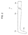
- a probe pin according to an embodiment of the present invention has a shape similar to the conventional probe pin. More specifically, the probe pin generally designated by numeral 16 has, consecutively as viewed from the card plate (not shown), a base portion 16a having a maximum diameter, a taper portion 16b extending in a slanted direction and having a smaller diameter toward the tip, a bend 16c having an angle somewhat more than 90 degrees, and a tip portion 16d extending substantially in the vertical direction.
- the probe pin 16 includes a metallic body or pin body 32 made of rhenium-containing tungsten, a plating film 34 made of nickel (Ni) formed on the metallic body 32 as an underlying plating film, and a non-oxidizable metallic film (overcoat) 36 made of a platinum group metal formed on the underlying plating film 34.
- the metallic body 32 is formed as a rhenium-containing tungsten wire having a diameter around 0.2 mm.
- the metallic body 32 may be made of tungsten or beryllium copper instead.
- the underlying plating film 34 is formed on the metallic body 32 to a thickness of 3 micrometers by an electric-plating process.
- the non-oxidizable metallic film 36 is made of rhodium having a thickness of 1 micrometer and formed by an electric-plating process. Rhodium is selected from the platinum group metals because rhodium achieves a stable contact with the chip electrodes and has a longer lifetime due to the following properties:
- the probe pins of the present embodiment are used in the typical probe card such as shown in Fig. 1.
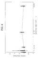
- Samples of the probe pin of the present embodiment were attached to card bodies for measurements of the characteristics of the embodiment after repetitive contact tests. The measurements were directed to the contact resistance between the samples and chip electrodes each including aluminum added with copper.
- the chip electrodes were formed on micro controller units (MCUs)
- the contact resistance was measured between each sample and the chip electrode after a first contact, after about 4 ⁇ 10 3 times, about 12.5 ⁇ 10 3 times, about 47.5 ⁇ 10 3 times, and about 110 ⁇ 10 3 times of repetitive contacts therebetween.
- the probe pins were not ground for cleaning during and between the measurements.
- Fig. 4 shows the results of the measurements, wherein the contact resistances thus measured are shown by circular dots, and the broken line represents the mean value thereof.
- the mean initial contact resistance was 1.0 ohm ( ⁇ ).
- Comparative samples of the conventional probe pin were also manufactured and subjected to similar measurements.
- the mean initial contact resistance of the comparative samples was 1.0 ohm; however, the contact resistances exceeded 2.5 ohms so that the electric characteristics of the semiconductor chips could not be measured after 5 ⁇ 10 3 times of repetitive contacts, and the measurements were stopped.
- the contact resistances measured for the comparative samples are shown by triangular dots and the mean contact resistance is shown by solid line in Fig. 4.
- the probe pin according to the embodiment had a contact resistance superior to the contact resistance of the conventional probe pin. More specifically, the samples of the present embodiment exhibited superior contact resistances lower than 1.5 ohms after 110 ⁇ 10 3 times of repetitive contacts, or after testing 110,000 semiconductor chips, whereas the comparative examples of the conventional probe pin failed after 5 ⁇ 10 3 times of repetitive contacts, or after testing 5000 semiconductor chips. Thus, it was concluded that the probe pin of the embodiment had a higher resistance against oxidation over the conventional probe pin.
- metallic bodies of probe pins are formed by taper-shaping a metallic wire made of rhenium tungsten, bending the tapered wire in the vicinity of the tip portion, and heat treating resultant wire to control the hardness thereof and remove the residual strain therein.
- step S2 the resultant metallic bodies of the probe pins 16 are attached and fixed using mold resin 24 onto a card plate 14, followed by forming an interconnect wire 26 on the card plate 14 for each of the probe pins 16.
- step S3 the tips of probe pins 16 are ground and polished to have a uniform height with respect to the bottom surface of the card plate 14.
- each metallic body of the probe pin 16 is plated with a 3- ⁇ m-thick underlying nickel film 34 and a 1- ⁇ m-thick rhodium film 36, as shown in Fig. 3.
- the electric plating system used in step S4 includes a plating bath 42 receiving therein plating liquid for plating the probe pins 32, a liquid circulating system including a tube 44 and a circular pump 46 disposed for the plating bath 42 for circulating the plating liquid therethrough, and an anode 48 opposing the probe pins 32 in the plating liquid for forming a pair of electrodes together with the probe pins constituting a cathode.
- the plating bath 42 has a fixing member 52 having a pair of jigs 50A and 50B for fixing therebetween the card plate 38 for immersing most parts of the probe pins 32 including the tips thereof in the plating liquid.
- the fixing member 52 has a pair of gaskets 54 and 56 between the jig 50A and the card plate 38 and between the jig 50B and the card plate 38, respectively, thereby preventing the plating liquid from escaping from the plating bath 42.
- the electric plating process using the electric plating system of Fig. 6 for forming the nickel film and the rhodium film includes the following steps:
- the rhodium may be replaced by another of platinum group metals including iridium (Ir), platinum (Pt) and ruthenium (Ru).
- platinum group metals including iridium (Ir), platinum (Pt) and ruthenium (Ru).
- a preferable thickness for the nickel plating film 34 resides between 2 and 4 micrometers.
- a thickness for the nickel plating film 34 below 2 micrometers has a limited function as the underlying layer.
- a thickness above 4 micrometers raises the cost of the probe card, while improving little in smoothing and barrier functions.
- a preferable thickness for the non-oxidizable metallic film 36 resides between 0.5 and 1.5 micrometers.
- a thickness for the non-oxidizable metallic film 36 below 0.5 micrometers affords a limited mechanical strength whereas a thickness above 1.5 micrometers raises the cost.
- the process for forming the nickel plating film 34 and the non-oxidizable metallic film 36 may preferably use a hot dipping or electric plating technique, the latter being more preferable.
Landscapes
- Physics & Mathematics (AREA)
- General Physics & Mathematics (AREA)
- Measuring Leads Or Probes (AREA)
- Testing Or Measuring Of Semiconductors Or The Like (AREA)
- Electroplating Methods And Accessories (AREA)
Abstract
Description
Claims (8)
- A probe pin for use in a probe card comprising a metallic body (32) and a non-oxidizable film (36) made of at least one of platinum group metals formed on said metallic plate (32), characterized by a nickel plating film (34) interposed between said metallic body (32) and said non-oxidizable film (36).
- The probe pin as defined in claim 1, wherein said non-oxidizable film (36) is a rhodium (Rh), iridium (Ir), platinum (Pt) or ruthenium (Ru) plating film.
- The probe pin as defined in claim 1, wherein said metallic body (32) is made of tungsten (W), rhenium-containing tungsten (ReW) or beryllium copper (BeCu).
- A probe card comprising a card plate (14) and a plurality of probe pins (16) fixed onto said card plate (14), each of said probe pins (16) including a metallic body (32), and a non-oxidizable film (36) made of at least one of platinum group metals formed on said metallic body (32), characterized by a nickel plating film (34) interposed between said metallic body (32) and said non-oxidizable film (36).
- The probe card as defined in claim 1, wherein said non-oxidizable film (36) is a rhodium (Rh), iridium (Ir), platinum (Pt) or ruthenium (Ru) plating film.
- The probe card as defined in claim 1, wherein said metallic body (32) is made of tungsten (W), rhenium-containing tungsten (ReW) or beryllium copper (BeCu).
- A method for fabricating a probe card comprising the steps of:forming a plurality of metallic bodies (32) by taper-shaping and bending metallic wires;fixing said metallic bodies (32) to a card plate (14), andpolishing tips of said metallic bodies (32) fixed onto said card plate (14) so that said metallic bodies (32) have a substantially uniform height with respect to a surface of said card plate (14); characterized by:plating said probe bodies (32) fixed onto said card plate to form consecutively a nickel plating film (34) and a non-oxidizable metallic plating film (36) on said metallic bodies (32).
- The method as defined in claim 7, wherein said plating steps uses a liquid flow in vicinities of tips of said metallic bodies (32).
Applications Claiming Priority (2)
| Application Number | Priority Date | Filing Date | Title |
|---|---|---|---|
| JP2000324031 | 2000-10-24 | ||
| JP2000324031A JP2002131334A (en) | 2000-10-24 | 2000-10-24 | Probe needle, probe card, and method of manufacturing probe card |
Publications (3)
| Publication Number | Publication Date |
|---|---|
| EP1202337A2 true EP1202337A2 (en) | 2002-05-02 |
| EP1202337A3 EP1202337A3 (en) | 2002-09-18 |
| EP1202337B1 EP1202337B1 (en) | 2006-06-14 |
Family
ID=18801622
Family Applications (1)
| Application Number | Title | Priority Date | Filing Date |
|---|---|---|---|
| EP01125135A Expired - Lifetime EP1202337B1 (en) | 2000-10-24 | 2001-10-23 | Fabrication of a probe card |
Country Status (6)
| Country | Link |
|---|---|
| US (1) | US6812723B2 (en) |
| EP (1) | EP1202337B1 (en) |
| JP (1) | JP2002131334A (en) |
| KR (1) | KR100551514B1 (en) |
| DE (1) | DE60120598T2 (en) |
| TW (1) | TW507309B (en) |
Cited By (2)
| Publication number | Priority date | Publication date | Assignee | Title |
|---|---|---|---|---|
| EP1717590A4 (en) * | 2004-12-14 | 2008-10-01 | Advantest Corp | Contact pin, probe card using same and electronic device testing apparatus |
| CN107881537A (en) * | 2017-03-22 | 2018-04-06 | 珠海市斗门区永兴盛金属塑料制品有限公司 | A kind of beryllium-copper surface plating ni-w-p alloy and preparation method thereof |
Families Citing this family (37)
| Publication number | Priority date | Publication date | Assignee | Title |
|---|---|---|---|---|
| WO2003005042A1 (en) * | 2001-07-02 | 2003-01-16 | Nhk Spring Co., Ltd. | Conductive contact |
| JP4045084B2 (en) * | 2001-08-17 | 2008-02-13 | 株式会社神戸製鋼所 | Electrical connection inspection device |
| US8225481B2 (en) * | 2003-05-19 | 2012-07-24 | Pratt & Whitney Rocketdyne, Inc. | Diffusion bonded composite material and method therefor |
| JP4723195B2 (en) * | 2004-03-05 | 2011-07-13 | 株式会社オクテック | Probe manufacturing method |
| US7023231B2 (en) * | 2004-05-14 | 2006-04-04 | Solid State Measurements, Inc. | Work function controlled probe for measuring properties of a semiconductor wafer and method of use thereof |
| KR20050123309A (en) * | 2004-06-24 | 2005-12-29 | 주식회사 새한마이크로텍 | Probe pin for examining semiconductor device |
| JP4523438B2 (en) * | 2005-02-03 | 2010-08-11 | 山一電機株式会社 | Probe unit, probe assembly, and electronic device inspection method |
| JP4216823B2 (en) * | 2005-03-04 | 2009-01-28 | 田中貴金属工業株式会社 | Probe pin and a blob card having the blob bin |
| JP4676224B2 (en) * | 2005-03-23 | 2011-04-27 | 東京特殊電線株式会社 | Probe needle and manufacturing method thereof |
| JP4584140B2 (en) * | 2005-12-26 | 2010-11-17 | 志忠 王 | Method for treating the surface of a probe needle installed on a probe card |
| KR101159074B1 (en) * | 2006-01-14 | 2012-06-25 | 삼성전자주식회사 | Conductive carbon nanotube tip, probe of scanning probe microscope comprising the same and manufacturing method of the conductive carbon nanotube tip |
| KR100764631B1 (en) * | 2006-04-13 | 2007-10-08 | (주)티에스이 | Probe tip round geometry machining method |
| US20080122470A1 (en) * | 2006-11-27 | 2008-05-29 | Wen-Yu Lu | Probe installed to a probe card |
| JP5046909B2 (en) | 2007-12-21 | 2012-10-10 | 株式会社日本マイクロニクス | Contact for electrical test, electrical connection device using the contact, and method for manufacturing contact |
| JP4213761B1 (en) * | 2008-02-27 | 2009-01-21 | 田中貴金属工業株式会社 | Iridium alloy with excellent hardness, workability, and antifouling properties |
| KR100949984B1 (en) * | 2008-06-30 | 2010-03-26 | 장경규 | Needle for probe card |
| KR100940010B1 (en) * | 2009-08-24 | 2010-02-03 | 이성광 | Manupacturing method of probe pin and thereby probe pin |
| JP5691193B2 (en) * | 2010-02-26 | 2015-04-01 | 富士通セミコンダクター株式会社 | Contactor, semiconductor device testing apparatus, and semiconductor device manufacturing method |
| JP2012037401A (en) * | 2010-08-09 | 2012-02-23 | Sankei Engineering:Kk | Inspection probe manufacturing method |
| CN102375080B (en) * | 2010-08-20 | 2014-08-13 | 旺矽科技股份有限公司 | Combined probe head |
| JP2012145490A (en) * | 2011-01-13 | 2012-08-02 | Sankei Engineering:Kk | Manufacturing method of inspection probe |
| JP5340462B2 (en) * | 2012-08-14 | 2013-11-13 | 株式会社サンケイエンジニアリング | Manufacturing method of inspection probe |
| TWI574013B (en) * | 2013-03-15 | 2017-03-11 | 穩懋半導體股份有限公司 | Probe card, probe structure and method for manufacturing the same |
| EP2894483B1 (en) | 2014-01-09 | 2018-06-27 | Multitest elektronische Systeme GmbH | Contact tip and contact element and method of producing the same |
| US10330701B2 (en) * | 2014-02-22 | 2019-06-25 | International Business Machines Corporation | Test probe head for full wafer testing |
| CN107257928B (en) * | 2014-12-30 | 2020-12-01 | 泰克诺探头公司 | Contact probes for test heads |
| CN106935524B (en) | 2015-12-24 | 2020-04-21 | 台湾积体电路制造股份有限公司 | Probe card and wafer testing system and wafer testing method |
| KR102072634B1 (en) * | 2018-10-17 | 2020-02-03 | 한국생산기술연구원 | Probe card needle with improved corrosion and electrical properties |
| JP7146663B2 (en) * | 2019-02-15 | 2022-10-04 | 株式会社荏原製作所 | Substrate holder and plating equipment |
| JP7633766B2 (en) * | 2019-11-11 | 2025-02-20 | 株式会社日本マイクロニクス | Electrical Connection Device |
| EP3862759B1 (en) * | 2020-02-04 | 2022-05-11 | Heraeus Deutschland GmbH & Co. KG | Sheathed wire and method for producing same |
| JP2022060711A (en) | 2020-10-05 | 2022-04-15 | 東京特殊電線株式会社 | Contact probe |
| JP2024506793A (en) * | 2021-02-22 | 2024-02-15 | エクサドン アーゲー | Method for making probe cards |
| KR102885632B1 (en) * | 2021-06-07 | 2025-11-13 | (주)포인트엔지니어링 | The Electro-conductive Contact Pin |
| CN114921839B (en) * | 2022-05-19 | 2023-11-10 | 强一半导体(苏州)股份有限公司 | Method for gold plating of probe tail and positioning jig |
| CN115029747A (en) * | 2022-07-26 | 2022-09-09 | 上海泽丰半导体科技有限公司 | A kind of probe processing method and probe |
| CN120652129B (en) * | 2025-08-19 | 2025-10-17 | 南京云极芯半导体科技有限公司 | Method for manufacturing probe tip of probe card |
Family Cites Families (32)
| Publication number | Priority date | Publication date | Assignee | Title |
|---|---|---|---|---|
| US900316A (en) * | 1907-05-04 | 1908-10-06 | Alexis Alexander Shukoff | Process of making terpene esters. |
| JPS5922810B2 (en) | 1977-07-19 | 1984-05-29 | カネボウ株式会社 | Manufacturing method of polyester sewing thread |
| US4837622A (en) * | 1985-05-10 | 1989-06-06 | Micro-Probe, Inc. | High density probe card |
| JPS63310977A (en) | 1987-02-25 | 1988-12-19 | Marubishi Kinzoku Kogyo Kk | Plated high-carbon wire to be formed into precise spring |
| JPH01138039A (en) | 1987-11-26 | 1989-05-30 | Kawasaki Steel Corp | Manufacture of rapidly cooled strip |
| JPH01169367A (en) | 1987-12-25 | 1989-07-04 | Sumitomo Electric Ind Ltd | Microelectrode resistance measurement probe |
| JPH01287484A (en) | 1988-05-16 | 1989-11-20 | Hitachi Ltd | Probe head, manufacturing method thereof, and semiconductor LSI inspection device using the same |
| JPH0212070A (en) | 1988-06-30 | 1990-01-17 | Toshiba Corp | Manufacture of inspection device |
| US5134365A (en) * | 1989-07-11 | 1992-07-28 | Nihon Denshizairyo Kabushiki Kaisha | Probe card in which contact pressure and relative position of each probe end are correctly maintained |
| JPH03180769A (en) | 1989-12-11 | 1991-08-06 | Kobe Steel Ltd | Probe for examination |
| JP2769015B2 (en) | 1990-03-08 | 1998-06-25 | 株式会社神戸製鋼所 | Prober pin head for electronic circuit board inspection and method of manufacturing the same |
| US5325052A (en) | 1990-11-30 | 1994-06-28 | Tokyo Electron Yamanashi Limited | Probe apparatus |
| JP2502231B2 (en) | 1991-12-17 | 1996-05-29 | 株式会社東京カソード研究所 | Probe card inspection device |
| DE4204244A1 (en) | 1992-02-13 | 1993-08-19 | Porsche Ag | DRIVE CONNECTION WITH TORQUE DAMPING IN THE DRIVETRAIN OF A MOTOR VEHICLE |
| JPH0795079B2 (en) | 1992-04-28 | 1995-10-11 | 日本電子材料株式会社 | Probe card |
| JPH05322930A (en) | 1992-05-15 | 1993-12-07 | Nippon Maikuronikusu:Kk | Probe assembly and manufacture thereof |
| JPH06249879A (en) | 1993-03-01 | 1994-09-09 | Kobe Steel Ltd | Manufacture of probe unit |
| JPH07248337A (en) | 1994-03-11 | 1995-09-26 | Okano Denki Kk | Contact probe |
| JPH09236619A (en) | 1996-02-29 | 1997-09-09 | Nippon Denshi Zairyo Kk | Vertical probe card |
| KR100212169B1 (en) | 1996-02-13 | 1999-08-02 | 오쿠보 마사오 | Probe, manufacture of same, and vertically operative type probe card assembly employing the same |
| DE19617488C2 (en) | 1996-05-02 | 2002-03-07 | Gustav Krueger | Contact element for detachable electrical connections |
| JPH1031034A (en) * | 1996-07-17 | 1998-02-03 | Denki Kagaku Kogyo Kk | Probe card with parallelism regulator |
| US5900316A (en) * | 1996-12-06 | 1999-05-04 | International Business Machines Corporation | Flexible conductive sheet |
| JP3279246B2 (en) | 1997-09-12 | 2002-04-30 | 三菱電機株式会社 | Semiconductor device test probe needle and method of manufacturing the same, probe device using this probe needle, method of testing semiconductor device with this probe needle, and semiconductor device tested with this probe needle |
| EP0893695B1 (en) | 1997-07-24 | 2005-10-26 | Mitsubishi Denki Kabushiki Kaisha | Test probe for semiconductor devices and method of manufacturing of the same |
| JP3164535B2 (en) | 1997-07-24 | 2001-05-08 | 日本電子材料株式会社 | How to modify the probe tip |
| US6891360B1 (en) | 1997-10-02 | 2005-05-10 | International Business Machines Corporation | Plated probe structure |
| JP3123483B2 (en) | 1997-10-28 | 2001-01-09 | 日本電気株式会社 | Probe card and probe card forming method |
| JP3458684B2 (en) | 1997-11-28 | 2003-10-20 | 三菱マテリアル株式会社 | Contact probe |
| JPH11273818A (en) | 1998-03-26 | 1999-10-08 | Matsushita Seisakusho:Kk | Contact socket for semiconductor element inspection |
| JP3180769B2 (en) | 1998-07-17 | 2001-06-25 | 日本電気株式会社 | Receiving power calculation method and mobile station |
| KR20000059158A (en) | 2000-07-19 | 2000-10-05 | 홍영희 | Probe, probe card and fabrication method of probe |
-
2000
- 2000-10-24 JP JP2000324031A patent/JP2002131334A/en active Pending
-
2001
- 2001-10-18 TW TW090125798A patent/TW507309B/en not_active IP Right Cessation
- 2001-10-23 DE DE60120598T patent/DE60120598T2/en not_active Expired - Fee Related
- 2001-10-23 US US09/983,171 patent/US6812723B2/en not_active Expired - Fee Related
- 2001-10-23 EP EP01125135A patent/EP1202337B1/en not_active Expired - Lifetime
- 2001-10-24 KR KR1020010065763A patent/KR100551514B1/en not_active Expired - Fee Related
Cited By (4)
| Publication number | Priority date | Publication date | Assignee | Title |
|---|---|---|---|---|
| EP1717590A4 (en) * | 2004-12-14 | 2008-10-01 | Advantest Corp | Contact pin, probe card using same and electronic device testing apparatus |
| US7667471B2 (en) | 2004-12-14 | 2010-02-23 | Advantest Corporation | Contact pin probe card and electronic device test apparatus using same |
| CN107881537A (en) * | 2017-03-22 | 2018-04-06 | 珠海市斗门区永兴盛金属塑料制品有限公司 | A kind of beryllium-copper surface plating ni-w-p alloy and preparation method thereof |
| CN107881537B (en) * | 2017-03-22 | 2019-07-02 | 珠海市斗门区永兴盛金属塑料制品有限公司 | A kind of beryllium-copper surface plating ni-w-p alloy and preparation method thereof |
Also Published As
| Publication number | Publication date |
|---|---|
| US20020047721A1 (en) | 2002-04-25 |
| TW507309B (en) | 2002-10-21 |
| EP1202337B1 (en) | 2006-06-14 |
| DE60120598D1 (en) | 2006-07-27 |
| JP2002131334A (en) | 2002-05-09 |
| KR20020032375A (en) | 2002-05-03 |
| DE60120598T2 (en) | 2007-06-14 |
| EP1202337A3 (en) | 2002-09-18 |
| KR100551514B1 (en) | 2006-02-13 |
| US6812723B2 (en) | 2004-11-02 |
Similar Documents
| Publication | Publication Date | Title |
|---|---|---|
| EP1202337B1 (en) | Fabrication of a probe card | |
| JP3745184B2 (en) | Probe for probe card and manufacturing method thereof | |
| US7311811B2 (en) | Device providing electrical contact to the surface of a semiconductor workpiece during processing | |
| JP3279294B2 (en) | Semiconductor device test method, semiconductor device test probe needle, method of manufacturing the same, and probe card provided with the probe needle | |
| US20020153913A1 (en) | Probe for the probe card | |
| JP5255459B2 (en) | Contact probe | |
| US8975908B2 (en) | Electrical test probe and probe assembly with improved probe tip | |
| KR20180057520A (en) | Probe for the test device | |
| JP6221031B1 (en) | Contact probe and electrical connection jig | |
| US8159248B2 (en) | Interposer structures and methods of manufacturing the same | |
| JP2992512B1 (en) | Probe card | |
| JP3745744B2 (en) | Method for producing metal structure and metal structure produced by the method | |
| JP2007155474A (en) | Probe and manufacturing method thereof | |
| JPH10221366A (en) | Probe pin and inspection device having the same | |
| JP2008096293A (en) | Manufacturing method of contact for inspection, contact for inspection, tool for inspection, and inspection device | |
| JP3391352B2 (en) | Probe needle for testing semiconductor device, manufacturing method thereof, and probe card provided with the probe needle | |
| JP2001116765A (en) | Probe card pin | |
| JP2002270654A (en) | Probe pin for probe card | |
| KR101164415B1 (en) | Probe card | |
| JP2003240800A (en) | Tee probe and probe card using this tee probe | |
| WO1986007205A1 (en) | Nickel-based electrical contact device | |
| CN121889523A (en) | Cu-Ag alloy wire and its manufacturing method | |
| JP2022060711A (en) | Contact probe | |
| JP2007256088A (en) | Probe pin | |
| JP2005008986A (en) | Metal structure and manufacturing method thereof |
Legal Events
| Date | Code | Title | Description |
|---|---|---|---|
| PUAI | Public reference made under article 153(3) epc to a published international application that has entered the european phase |
Free format text: ORIGINAL CODE: 0009012 |
|
| AK | Designated contracting states |
Kind code of ref document: A2 Designated state(s): AT BE CH CY DE DK ES FI FR GB GR IE IT LI LU MC NL PT SE TR |
|
| AX | Request for extension of the european patent |
Free format text: AL;LT;LV;MK;RO;SI |
|
| PUAL | Search report despatched |
Free format text: ORIGINAL CODE: 0009013 |
|
| AK | Designated contracting states |
Kind code of ref document: A3 Designated state(s): AT BE CH CY DE DK ES FI FR GB GR IE IT LI LU MC NL PT SE TR |
|
| AX | Request for extension of the european patent |
Free format text: AL;LT;LV;MK;RO;SI |
|
| 17P | Request for examination filed |
Effective date: 20020905 |
|
| 17Q | First examination report despatched |
Effective date: 20030109 |
|
| RAP1 | Party data changed (applicant data changed or rights of an application transferred) |
Owner name: NEC ELECTRONICS CORPORATION |
|
| AKX | Designation fees paid |
Designated state(s): DE FR |
|
| RTI1 | Title (correction) |
Free format text: FABRICATION OF A PROBE CARD |
|
| GRAP | Despatch of communication of intention to grant a patent |
Free format text: ORIGINAL CODE: EPIDOSNIGR1 |
|
| GRAS | Grant fee paid |
Free format text: ORIGINAL CODE: EPIDOSNIGR3 |
|
| GRAA | (expected) grant |
Free format text: ORIGINAL CODE: 0009210 |
|
| AK | Designated contracting states |
Kind code of ref document: B1 Designated state(s): DE FR |
|
| REF | Corresponds to: |
Ref document number: 60120598 Country of ref document: DE Date of ref document: 20060727 Kind code of ref document: P |
|
| ET | Fr: translation filed | ||
| PLBE | No opposition filed within time limit |
Free format text: ORIGINAL CODE: 0009261 |
|
| STAA | Information on the status of an ep patent application or granted ep patent |
Free format text: STATUS: NO OPPOSITION FILED WITHIN TIME LIMIT |
|
| 26N | No opposition filed |
Effective date: 20070315 |
|
| PGFP | Annual fee paid to national office [announced via postgrant information from national office to epo] |
Ref country code: DE Payment date: 20081016 Year of fee payment: 8 |
|
| PGFP | Annual fee paid to national office [announced via postgrant information from national office to epo] |
Ref country code: FR Payment date: 20081014 Year of fee payment: 8 |
|
| REG | Reference to a national code |
Ref country code: FR Ref legal event code: ST Effective date: 20100630 |
|
| PG25 | Lapsed in a contracting state [announced via postgrant information from national office to epo] |
Ref country code: DE Free format text: LAPSE BECAUSE OF NON-PAYMENT OF DUE FEES Effective date: 20100501 Ref country code: FR Free format text: LAPSE BECAUSE OF NON-PAYMENT OF DUE FEES Effective date: 20091102 |