EP1201412A2 - Verfahren zur Herstellung von einer Mikrolinse und einer Mikrolinseanordnung - Google Patents
Verfahren zur Herstellung von einer Mikrolinse und einer Mikrolinseanordnung Download PDFInfo
- Publication number
- EP1201412A2 EP1201412A2 EP01203995A EP01203995A EP1201412A2 EP 1201412 A2 EP1201412 A2 EP 1201412A2 EP 01203995 A EP01203995 A EP 01203995A EP 01203995 A EP01203995 A EP 01203995A EP 1201412 A2 EP1201412 A2 EP 1201412A2
- Authority
- EP
- European Patent Office
- Prior art keywords
- microlens
- substrate
- mold
- mold cavity
- cutting member
- Prior art date
- Legal status (The legal status is an assumption and is not a legal conclusion. Google has not performed a legal analysis and makes no representation as to the accuracy of the status listed.)
- Withdrawn
Links
Images


Classifications
-
- G—PHYSICS
- G02—OPTICS
- G02B—OPTICAL ELEMENTS, SYSTEMS OR APPARATUS
- G02B3/00—Simple or compound lenses
-
- B—PERFORMING OPERATIONS; TRANSPORTING
- B29—WORKING OF PLASTICS; WORKING OF SUBSTANCES IN A PLASTIC STATE IN GENERAL
- B29C—SHAPING OR JOINING OF PLASTICS; SHAPING OF MATERIAL IN A PLASTIC STATE, NOT OTHERWISE PROVIDED FOR; AFTER-TREATMENT OF THE SHAPED PRODUCTS, e.g. REPAIRING
- B29C33/00—Moulds or cores; Details thereof or accessories therefor
- B29C33/38—Moulds or cores; Details thereof or accessories therefor characterised by the material or the manufacturing process
- B29C33/3842—Manufacturing moulds, e.g. shaping the mould surface by machining
-
- B—PERFORMING OPERATIONS; TRANSPORTING
- B29—WORKING OF PLASTICS; WORKING OF SUBSTANCES IN A PLASTIC STATE IN GENERAL
- B29C—SHAPING OR JOINING OF PLASTICS; SHAPING OF MATERIAL IN A PLASTIC STATE, NOT OTHERWISE PROVIDED FOR; AFTER-TREATMENT OF THE SHAPED PRODUCTS, e.g. REPAIRING
- B29C45/00—Injection moulding, i.e. forcing the required volume of moulding material through a nozzle into a closed mould; Apparatus therefor
- B29C45/17—Component parts, details or accessories; Auxiliary operations
- B29C45/26—Moulds
- B29C45/37—Mould cavity walls, i.e. the inner surface forming the mould cavity, e.g. linings
- B29C45/372—Mould cavity walls, i.e. the inner surface forming the mould cavity, e.g. linings provided with means for marking or patterning, e.g. numbering articles
-
- B—PERFORMING OPERATIONS; TRANSPORTING
- B29—WORKING OF PLASTICS; WORKING OF SUBSTANCES IN A PLASTIC STATE IN GENERAL
- B29D—PRODUCING PARTICULAR ARTICLES FROM PLASTICS OR FROM SUBSTANCES IN A PLASTIC STATE
- B29D11/00—Producing optical elements, e.g. lenses or prisms
- B29D11/00009—Production of simple or compound lenses
- B29D11/00278—Lenticular sheets
-
- B—PERFORMING OPERATIONS; TRANSPORTING
- B29—WORKING OF PLASTICS; WORKING OF SUBSTANCES IN A PLASTIC STATE IN GENERAL
- B29D—PRODUCING PARTICULAR ARTICLES FROM PLASTICS OR FROM SUBSTANCES IN A PLASTIC STATE
- B29D11/00—Producing optical elements, e.g. lenses or prisms
- B29D11/00009—Production of simple or compound lenses
- B29D11/00365—Production of microlenses
-
- B—PERFORMING OPERATIONS; TRANSPORTING
- B29—WORKING OF PLASTICS; WORKING OF SUBSTANCES IN A PLASTIC STATE IN GENERAL
- B29L—INDEXING SCHEME ASSOCIATED WITH SUBCLASS B29C, RELATING TO PARTICULAR ARTICLES
- B29L2011/00—Optical elements, e.g. lenses, prisms
- B29L2011/0016—Lenses
Definitions
- the invention relates generally to the field of improved microlens molds and microlens. More particularly, the invention concerns a method of making a precision mold suitable for forming high quality, micro-sized optical articles, such as a microlens or microlens array.
- Rotationally symmetric optical surfaces in molds for injection molding or compression molding are typically made either by grinding or diamond turning. While these techniques work well for larger surfaces, they are not suited for making high quality optical surfaces in small sizes or arrays. Other techniques are available for making small scale single lenses and arrays but they are limited as to fill factor, optical accuracy and/or the height or sag of the lens geometry that can be made.
- Diamond turning can be used to make optical surfaces down to 2 millimeters in size but the setup is difficult. Precise location of multiple optical surfaces is not possible due to multiple setups. The need for multiple setups also increases the machining time for an array so that diamond turning becomes cost prohibitive.
- polymer reflow Another technique that is suitable for making microlenses under 2 millimeters is polymer reflow.
- Polymer reflow is done by depositing drops of polymer onto a surface and then heating the polymer to allow it to melt and reflow into a spherical shape under the influence of surface tension effects.
- reflow lenses can be separated from one another so that they contact the underlying surface in a round pattern. To maintain round pattern of each lens at the surface, the lenses can be separated from one another which substantially limits the fill factor in an array.
- Grayscale lithography is also useable for making microlenses under 2 millimeters. Grayscale lithography can be used to make nearly any shape and high fill factors can be produced in lens arrays. However, reactive ion beam etching and other etching techniques that are used in gray scale lithography are limited as to the depth that can be accurately produced with an optical surface, typically the sag is limited to under 30 micron.
- High sag lenses are typically associated with high magnification or high power refractive lenses that are used for imaging.
- High power refractive lenses have tight curvature and steep sides to maximize the included angle and associated light gathering or light spreading which implies a high sag.
- refractive lenses are preferred to preserve the wave front of the image.
- Fresnel or diffractive lenses where the optical curve is cut into segmented rings can be used to reduce the overall sag of the lens.
- high power diffractive lenses are not feasible due to the steepness and narrow spacing of the ring segments at the edge that would be required to make a low sag, high power microlens.
- the present invention has the following advantages: the precision microlens mold can be used to mold high quality, micro-sized optical articles, such as microlenses, that have symmetric surfaces with steep sides and high sags; and, the forming element is contoured to produce very accurate optical surfaces in single microlenses or arrays. In the case of arrays, near 100% fill factor can be achieved in the molded article.
- microlens mold 10 has a plurality of interconnecting square intersection micro-sized mold cavities 12 formed in substrate 14, as described more fully below.
- microlens mold 16 has a plurality of interconnecting hexagonal shaped intersection micro-sized mold cavities 18 formed in substrate 14, also described more fully below.
- microlens mold 20 has either a single micro-sized mold cavity (not shown) or a plurality of randomly distributed micro-sized mold cavities 22 formed in substrate 14, as described below.
- Substrate 14, in which the precision microlens molds 10, 16, 20 used in the invention are formed, may be made of any material that is compatible with very hard cutting tools, such as a diamond milling tool.
- substrate 14 includes materials selected from among copper, nickel, nickel alloy, nickel plating, brass, and silicon, with hardened nickel plating being most preferred.
- microlens mold 10, 16, 20 have been developed using the novel diamond milling method used in the invention.
- a spherical forming element 24 having a half radius diamond cutting member 26 is used to form the mold cavities 12, 18, 22 in the respective substrate 14 of microlens mold 10, 16, 20, by diamond milling into substrate 14.
- Diamond cutting member 26 has a substantially planar first face 28, a substantially planar second face 30 orthogonal to and intersecting first face 28, and a spherical contoured shaped cutting face 32 intersecting both the first and second face 28, 30 (respectively).
- First face 28 defines the rotational axis 34 of diamond cutting member 26 when operably connected to control member 36 and affixed for milling substrate 14, described below.
- Forming element 24 may be used to form a spherical microlens mold 10, 16 or 20 in substrate 14 (FIGS. 1-3). Spherical microlens mold 10, 16 or 20 is used for making spherical microlens articles.
- an alternative aspheric forming element 40 has an aspheric diamond cutting member 41.
- Diamond cutting member 41 has a substantially planar first face 42, a substantially planar second face 46 orthogonal and intersecting first face 42 and an aspheric cutting face 44 adjoining both first and second face 42, 46 (respectively).
- First face 42 defines the rotational axis 49 of diamond cutting member 41 when operably connected to control member 48 and affixed for milling substrate 14, described below.
- Forming element 40 having control member 48 may be used to form an aspheric microlens mold 10, 16 or 20 in substrate 14 (FIGS. 1-3). Aspheric microlens mold 10, 16 or 20 is used for making aspheric microlens articles.
- apparatus 50 for forming a precision single microlens mold (of the type shown in FIGS. 1-3) for a micro-sized optical article includes a forming element 24 or 40 operably connected to tool holder 56 and rotating control member 58.
- Forming element 24 or 40 has a rotatable hardened cutting member 26 or 41, preferably diamond (shown clearly in FIGS. 4 and 5), fixedly aligned relative to a linearly displaceable (noted by arrow Z) substrate 14.
- Substrate 14, operably connected to control member 64, is arranged for movement towards and away from hardened cutting member 26 or 41, as described above.
- Control member 36 or 48, forming element 24 or 40, and control member 64 are preferably all parts of a precision air bearing lathe such as is available from Precitech, Inc., located in Keene, New Hampshire, which is expressly designed for diamond turning of high precision parts.
- apparatus 50 can mill a predetermined shaped single microlens mold 52 in the substrate 14.
- Platform 54 is used to provide a solid, non-vibrating base for supporting apparatus 50 with both forming element 24 or 40 and substrate 14 during the mold forming process.
- substrate 14 is preferably mounted for movement relative to fixed forming element 24 or 40.
- apparatus 50 forms a single microlens mold 52 in substrate 14, as discussed above.
- apparatus 60 has a substrate 14 mounted for three-dimensional movement for forming a microlens mold array 62.
- Flexibly moveable substrate 14 is operably connected to control member 64 that governs the movements of substrate 14.
- the control member 64 in this case preferably has the ability of precision controlled movement of substrate 14 in the directions X-Y-Z as indicated in FIG. 7.
- Precision air bearing lathes with precision X-Y-Z table movement are available from Precitech, Inc., located in Keene, New Hampshire.
- control member 64 The X-Y-Z table movement of control member 64 is used to produce the flexible movements of substrate 14 relative to forming element 24 or 40.
- a tool holder 56 fixedly attached to rotating control member 58, such as the ones described above, having diamond cutting member 26 or 41 (as described above) is positioned for milling microlens array mold 62 in substrate 14.
- an array of microlens mold cavities can be formed in substrate 14.
- Movable substrate 14 is first positioned to mill one of a plurality of microlens mold cavities 62a in the microlens array mold 62.
- forming element 24 or 40 is removed from the mold cavity 62a and then the substrate 14 is moved laterally (X-Y) by control member 64 to another position for forming another microlens mold cavity 62b. This procedure is repeated until the desired number of microlens mold cavities in the microlens array mold 62 is formed in substrate 14.
- apparatus 60 having a movable substrate 14 can produce a high quality microlens array mold 62, such as those illustrated in FIGS. 1-3.
- any rotationally symmetric optical surface such as a microlens surface
- Spherical surfaces are produced using a half radius diamond with a circular segment diamond.
- Aspheres can be produced by using a diamond with an aspheric cutting edge.
- some rotationally non-symmetric lens surfaces such as anamorphic surfaces, can be made using a modified version of the technique described.
- the diamond tooling is moved laterally during the cutting action to create an elongated version of the spherical or aspheric surface.
- the right combination of diamond cutting member 26 or 41 rotational speed, feed i.e., the rate that diamond cutting member 26 or 41 penetrates substrate 14, and lubrication can be used to obtain the cleanest cut.
- forming element 24 or 40, shown with diamond cutting member 26 or 41 can be produced in such a manner that a sufficient clearance 70 is provided on the back side 72 of the diamond cutting member 26 or 41 to avoid drag marks on substrate 14. Drag marks (not shown) typically result from interference of the backside 72 of diamond cutting member 26 or 41 with the substrate 14 during the formation of microlens mold 76.
- microlens molds have been made down to 30 microns in diameter with irregularity of better than 0.50 wave (.25 micron). Further, microlens mold arrays have been made up to 80 X 80 microlenses with a 250 micron pitch in an orthogonal layout and a near 100% fill factor.
- aspheric lens surfaces can also be produced using this technique.
- an aspheric diamond cutting member 41 (FIG. 5) is all that is required to make rotationally symmetric aspheric lens surfaces.
- Anamorphic lens surfaces can be made as well using a modified version of this technique. In this case, the same or similar diamond cutting member 41 is moved laterally during the cutting operation to produce an elongated lens surface.
- the precision molds 10, 16, 20 (FIGS. 1-3) made with the methods and apparatus 50 or 60 used in the invention, can be used to manufacture large numbers of optical articles, such as microlenses.
- injection molding and compression molding are the preferred molding methods for forming the typically glass or plastic microlenses. In some cases casting is the preferred method.
- Apparatus for molding a two-sided microlens array 80 is composed of two large blocks or mold bases 82 each having an active molding face 83. Mold bases 82 are comprised typically of steel or other metal. Alignment members arranged on molding faces 83 include guide pins 88, tapered locating bushings 86 and corresponding apertures (not shown) for receiving guide pins 88 and tapered locating bushings 86.
- the microlens molds 84 and the mold cavities 85 were made according to the methods and apparatus used in the invention. Referring to FIG.
- the apparatus 80 comprises mold bases 82 which are installed into one of two platens 104, 106 of a hydraulic, pneumatic or electrically driven press 108.
- One side of the apparatus 80 is connected to one platen 104 of the press 108 and the other side is connected to the other platen 106.
- the guide pins 88 help to align the two sides of the mold base 82.
- the tapered locating bushings 86 align the two sides of the mold base 82 and the microlens molds 84 with each other. In the case of molding a two-sided microlens array, it is very important that the microlens surfaces on the opposing sides are aligned with each other.
- the microlens molds 84 are typically made on square substrates 100 (as shown in FIG. 10) so that they cannot rotate in the mold base 82.
- a hot plastic preform is inserted into the heated mold cavity.
- the press and mold base is then closed which compresses the plastic preform and forms the plastic to the shape of the mold cavity and microlens array mold.
- the mold and plastic is then cooled, the press and mold base is opened and the molded microlens array is removed from the mold.
- the opposing side from the microlens mold is typically a plano surface and then, since side-to-side and rotational alignment is not an issue, the microlens mold may be made onto a round substrate.
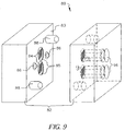
- Figure 10 shows the microlens array mold 96 (also shown in FIG. 9) with a square substrate 100 as is typically used to prevent rotation of the microlens array mold surface 98 in the mold base 82 of apparatus 80.
- the microlens array mold surface 98, the depth of the mold cavity 85 and the thickness of the molded microlens array article are determined precisely by adjusting the overall height of the substrate 100 and the height of the larger round substrate 102 on the bottom of the substrate 100.
- the material is simply poured into the mold cavity and allowed to solidify by chemical reaction rather than cooling. After the part has solidified, the part is removed from the mold.
- microlens molds made according to the invention have been used to injection mold microlens surfaces in which the sag is not limited, as indicated below. Further, near hemispheric lenses can be produced with very steep sidewalls. Also, it is our experience that optical surfaces can be machined directly into mold materials such as nickel, copper, aluminum, brass, nickel plating, or silicon.
- apparatus 50, 60 having a forming element 24, 40 with diamond cutting member 26, 41 (respectively) is quite accurate, it is our experience that lens surfaces can be produced in sizes down to 10 micron or less in diameter and 2 micron sag. Lenses up to 25 mm in diameter are also possible with sags of over 12.5 mm.
- microlenses made with the method and apparatus used in the invention.
- a microlens array mold with 80X80 microlenses was made in aluminum.
- the half radius diamond tool was obtained from ST&F Precision Technologies and Tools, located in Arden, North Carolina.
- the microlens surfaces were 0.250 mm across positioned in a square intersection array.
- the microlenses surfaces were spherical in curvature with a radius of 0.500 mm and a sag of 33 micron.
- centering of the diamond cutting member 26 in the control member 36 was done using an iterative process where a test cut was examined under the microscope and adjustments of the location of diamond cutting member 26 were made based on the size of the center defect. Rotational speed of diamond cutting member 26 used was 1000 rpm.
- Cutting fluid was purified mineral oil. The result of this process was a center defect of the machined mold of 2 micron and surface irregularity of I Wave (0.5 micron). Parts were subsequently injection molded, using the machined mold surface, to produce polymethylmethacrylate microlens arrays.
- Example 2 Similar to Example 1 with the exception that a hardened nickel-plated substrate was used for the machined mold surface.
- a microlens array mold with 13X13 microlenses surfaces was made in a hardened nickel-plated substrate.
- the microlens surfaces were 1.30 mm across positioned in a square intersection array.
- the half radius diamond tool was obtained from ST&F Precision Technologies and Tools, located in Arden, North Carolina.
- the microlens surfaces were spherical in curvature with a radius of 3.20 mm and a sag of 213 micron. Centering and the machining process were the same as described in Example 1. The result was a center defect of 1.5 micron with a surface irregularity of 0.30 Wave (0.15 micron).
- a series of single microlens surfaces was made in a 715 nickel alloy substrate.
- the microlens surfaces all were made with a 0.500 mm radius diamond tool. Diameters varied from 0.062 mm to 0.568 mm.
- the machining process was similar to that described in Example 1.
- a larger microlens array of 63.5 X 88.9 mm was made with 21,760 microlenses in total in a 125 X 175 square intersection array.
- a diamond half radius tool with a 0.5008 mm radius was used, obtained from Chardon Tool, Inc., located in Chardon, Ohio.
- the array was made with a 0.50932 pitch and a 0.16609 sag.
- the substrate was nickel-plated steel. The machining process was similar to that described in Example 1.
- two-sided microlens arrays can be molded in large numbers.
- two matched microlens array surfaces were made in hardened nickel-plated substrates.
- the half radius diamond tool or diamond cutting member 26 (FIG. 4) was obtained from Contour Fine Tooling, Inc., located in Marlborough, New Hampshire.
- the microlens surfaces were made with a 1.475 mm radius and a 0.750 mm pitch in a square intersection pattern, the sag was 99 micron.
- the machining process was similar to that described in Example 1. A center defect of 2 micron and an irregularity of 0.3 Wave (0.15 micron) were achieved in the machined surface.
- the two matched microlens array surfaces were mounted in a mold base so that they were opposed.
- the microlens surfaces were machined into square substrates prior to mounting into a mold base thereby inhibiting rotational misalignment.
- Taper lock bushings were then used to prevent lateral misalignment.
- two-sided microlens arrays were injection molded from polymethylmethacrylate. The molded microlenses on the two-sided array were aligned with each other within 30 micron.
Applications Claiming Priority (2)
| Application Number | Priority Date | Filing Date | Title |
|---|---|---|---|
| US09/702,951 US6402996B1 (en) | 2000-10-31 | 2000-10-31 | Method of manufacturing a microlens and a microlens array |
| US702951 | 2000-10-31 |
Publications (2)
| Publication Number | Publication Date |
|---|---|
| EP1201412A2 true EP1201412A2 (de) | 2002-05-02 |
| EP1201412A3 EP1201412A3 (de) | 2003-11-05 |
Family
ID=24823299
Family Applications (1)
| Application Number | Title | Priority Date | Filing Date |
|---|---|---|---|
| EP01203995A Withdrawn EP1201412A3 (de) | 2000-10-31 | 2001-10-19 | Verfahren zur Herstellung von einer Mikrolinse und einer Mikrolinseanordnung |
Country Status (5)
| Country | Link |
|---|---|
| US (1) | US6402996B1 (de) |
| EP (1) | EP1201412A3 (de) |
| JP (1) | JP2002192568A (de) |
| KR (1) | KR20020034922A (de) |
| TW (1) | TW523459B (de) |
Cited By (1)
| Publication number | Priority date | Publication date | Assignee | Title |
|---|---|---|---|---|
| EP1358992A1 (de) * | 2002-05-02 | 2003-11-05 | Orga Kartensysteme GmbH | Spritzgusswerkzeug zur Herstellung einer Chipkarte sowie ein Verfahren zur Herstellung einer Chipkarte |
Families Citing this family (12)
| Publication number | Priority date | Publication date | Assignee | Title |
|---|---|---|---|---|
| US6491481B1 (en) * | 2000-10-31 | 2002-12-10 | Eastman Kodak Company | Method of making a precision microlens mold and a microlens mold |
| US6908266B1 (en) * | 2000-10-31 | 2005-06-21 | Eastman Kodak Company | Apparatus for forming a microlens array mold |
| US6846137B1 (en) * | 2000-10-31 | 2005-01-25 | Eastman Kodak Company | Apparatus for forming a microlens mold |
| US20030025227A1 (en) * | 2001-08-02 | 2003-02-06 | Zograph, Llc | Reproduction of relief patterns |
| US6597510B2 (en) * | 2001-11-02 | 2003-07-22 | Corning Incorporated | Methods and apparatus for making optical devices including microlens arrays |
| JP3987503B2 (ja) * | 2004-03-11 | 2007-10-10 | 福島県 | 内面拡散反射体を形成するための母型の製造方法及び内面拡散反射体 |
| JP4340199B2 (ja) * | 2004-07-09 | 2009-10-07 | セイコーエプソン株式会社 | 有機エレクトロルミネッセンス装置の製造方法 |
| DE102004041272B4 (de) * | 2004-08-23 | 2017-07-13 | General Electric Technology Gmbh | Hybridbrennerlanze |
| JP5017798B2 (ja) * | 2005-04-20 | 2012-09-05 | コニカミノルタアドバンストレイヤー株式会社 | ピックアップ光学系に用いられる整形素子を成形する成形装置および該装置により製造された整形素子 |
| KR101147088B1 (ko) * | 2005-06-30 | 2012-05-17 | 엘지디스플레이 주식회사 | 화상전환용 액정표시소자 |
| US7434299B1 (en) | 2007-11-28 | 2008-10-14 | Sandia Corporation | Methods for the precise locating and forming of arrays of curved features into a workpiece |
| GB201418180D0 (en) * | 2014-10-14 | 2014-11-26 | Univ Surrey | Optical element for super-resolution imaging and fabrication method thereof |
Citations (6)
| Publication number | Priority date | Publication date | Assignee | Title |
|---|---|---|---|---|
| GB1203357A (en) * | 1968-12-13 | 1970-08-26 | Rlm Res Corp | Production of lenticular sheets for integral photography |
| US3548041A (en) * | 1966-07-07 | 1970-12-15 | Richard Steding | Lens mold making by plating lenticulations on a masked conductive support |
| JPS59140029A (ja) * | 1983-01-31 | 1984-08-11 | Sony Corp | マイクロレンズの製造方法 |
| WO1996007523A1 (en) * | 1994-09-09 | 1996-03-14 | Philips Electronics N.V. | Method of manufacturing a mould for use in the manufacture of an optical element comprising optical sub-elements mutually arranged in a pattern, and device for implementing such a method |
| EP0786326A1 (de) * | 1996-01-26 | 1997-07-30 | INSTITUT FÜR MIKROTECHNIK MAINZ GmbH | Verfahren und Vorrichtung zur Herstellung von optischen Linsen und optischen Linsenarrays |
| FR2752949A1 (fr) * | 1996-09-05 | 1998-03-06 | Anizan Paul | Procede de fabrication d'une matrice de micro-lentilles |
Family Cites Families (18)
| Publication number | Priority date | Publication date | Assignee | Title |
|---|---|---|---|---|
| US4198182A (en) * | 1975-09-20 | 1980-04-15 | Lucas Industries Limited | Method of manufacturing a mould for producing a lamp lens element |
| GB1546805A (en) * | 1975-09-20 | 1979-05-31 | Lucas Industries Ltd | Method of manufacturing a mould for producing a lens element and mould manufactured by that method |
| JPS59214510A (ja) * | 1983-05-19 | 1984-12-04 | Toshiba Tungaloy Co Ltd | ボ−ルエンドミル |
| JPH01271130A (ja) * | 1988-04-20 | 1989-10-30 | Asahi Optical Co Ltd | 樹脂製光学素子の非球面金型加工方法 |
| US5298366A (en) * | 1990-10-09 | 1994-03-29 | Brother Kogyo Kabushiki Kaisha | Method for producing a microlens array |
| JPH05217498A (ja) * | 1992-02-03 | 1993-08-27 | Hitachi Ltd | 螢光面パターン形成用補正レンズとその成形方法、およびその金型と金型の加工方法並びに加工装置 |
| JPH06118204A (ja) * | 1992-10-07 | 1994-04-28 | Hitachi Ltd | プラスチックマイクロレンズアレイ |
| US5300263A (en) | 1992-10-28 | 1994-04-05 | Minnesota Mining And Manufacturing Company | Method of making a microlens array and mold |
| US5439621A (en) * | 1993-04-12 | 1995-08-08 | Minnesota Mining And Manufacturing Company | Method of making an array of variable focal length microlenses |
| US5536455A (en) | 1994-01-03 | 1996-07-16 | Omron Corporation | Method of manufacturing lens array |
| JP3305120B2 (ja) * | 1994-06-30 | 2002-07-22 | キヤノン株式会社 | 光学素子の成形用型部材の加工方法 |
| JPH09131656A (ja) * | 1995-11-07 | 1997-05-20 | Fuji Xerox Co Ltd | 微小切削工具、その製造方法及び微小構造体の製造方法 |
| JPH09216232A (ja) * | 1996-02-09 | 1997-08-19 | Matsushita Electric Ind Co Ltd | 光学素子成形用金型およびその製造方法 |
| JPH10166368A (ja) * | 1996-12-10 | 1998-06-23 | Nikon Corp | 成形用金型の製造方法および成形用金型 |
| JPH11179601A (ja) * | 1997-12-18 | 1999-07-06 | Toshiba Corp | 加工装置とその加工方法およびその加工方法による光学部品 |
| JPH11207751A (ja) * | 1998-01-20 | 1999-08-03 | Nikon Corp | マイクロレンズアレイ成形用金型とその製造方法およびマイクロレンズアレイ |
| JPH11277543A (ja) * | 1998-03-27 | 1999-10-12 | Sharp Corp | マイクロレンズアレイ成形用金型の作製方法 |
| JPH11300757A (ja) * | 1998-04-23 | 1999-11-02 | Nikon Corp | トーリック凹面形状の形成方法と装置 |
-
2000
- 2000-10-31 US US09/702,951 patent/US6402996B1/en not_active Expired - Fee Related
-
2001
- 2001-09-06 TW TW090122112A patent/TW523459B/zh not_active IP Right Cessation
- 2001-10-19 EP EP01203995A patent/EP1201412A3/de not_active Withdrawn
- 2001-10-25 JP JP2001327573A patent/JP2002192568A/ja active Pending
- 2001-10-30 KR KR1020010067105A patent/KR20020034922A/ko not_active Application Discontinuation
Patent Citations (6)
| Publication number | Priority date | Publication date | Assignee | Title |
|---|---|---|---|---|
| US3548041A (en) * | 1966-07-07 | 1970-12-15 | Richard Steding | Lens mold making by plating lenticulations on a masked conductive support |
| GB1203357A (en) * | 1968-12-13 | 1970-08-26 | Rlm Res Corp | Production of lenticular sheets for integral photography |
| JPS59140029A (ja) * | 1983-01-31 | 1984-08-11 | Sony Corp | マイクロレンズの製造方法 |
| WO1996007523A1 (en) * | 1994-09-09 | 1996-03-14 | Philips Electronics N.V. | Method of manufacturing a mould for use in the manufacture of an optical element comprising optical sub-elements mutually arranged in a pattern, and device for implementing such a method |
| EP0786326A1 (de) * | 1996-01-26 | 1997-07-30 | INSTITUT FÜR MIKROTECHNIK MAINZ GmbH | Verfahren und Vorrichtung zur Herstellung von optischen Linsen und optischen Linsenarrays |
| FR2752949A1 (fr) * | 1996-09-05 | 1998-03-06 | Anizan Paul | Procede de fabrication d'une matrice de micro-lentilles |
Non-Patent Citations (1)
| Title |
|---|
| PATENT ABSTRACTS OF JAPAN vol. 008, no. 267 (M-343), 7 December 1984 (1984-12-07) & JP 59 140029 A (SONY KK), 11 August 1984 (1984-08-11) * |
Cited By (1)
| Publication number | Priority date | Publication date | Assignee | Title |
|---|---|---|---|---|
| EP1358992A1 (de) * | 2002-05-02 | 2003-11-05 | Orga Kartensysteme GmbH | Spritzgusswerkzeug zur Herstellung einer Chipkarte sowie ein Verfahren zur Herstellung einer Chipkarte |
Also Published As
| Publication number | Publication date |
|---|---|
| TW523459B (en) | 2003-03-11 |
| US6402996B1 (en) | 2002-06-11 |
| KR20020034922A (ko) | 2002-05-09 |
| JP2002192568A (ja) | 2002-07-10 |
| EP1201412A3 (de) | 2003-11-05 |
Similar Documents
| Publication | Publication Date | Title |
|---|---|---|
| US6476971B1 (en) | Method of manufacturing a microlens array mold and a microlens array | |
| US6787072B2 (en) | Apparatus and method for making a double-sided microlens mold and microlens array mold | |
| US6402996B1 (en) | Method of manufacturing a microlens and a microlens array | |
| US6491481B1 (en) | Method of making a precision microlens mold and a microlens mold | |
| US6597510B2 (en) | Methods and apparatus for making optical devices including microlens arrays | |
| CA2145683C (en) | Method of making plastic molds and process for cast molding contact lenses | |
| CA2497175C (en) | Method and mold for making ophthalmic devices | |
| US20030025227A1 (en) | Reproduction of relief patterns | |
| US6908266B1 (en) | Apparatus for forming a microlens array mold | |
| US6846137B1 (en) | Apparatus for forming a microlens mold | |
| EP1202080A2 (de) | Beidseitige Mikrolinsenanordnung |
Legal Events
| Date | Code | Title | Description |
|---|---|---|---|
| PUAI | Public reference made under article 153(3) epc to a published international application that has entered the european phase |
Free format text: ORIGINAL CODE: 0009012 |
|
| AK | Designated contracting states |
Kind code of ref document: A2 Designated state(s): AT BE CH CY DE DK ES FI FR GB GR IE IT LI LU MC NL PT SE TR |
|
| AX | Request for extension of the european patent |
Free format text: AL;LT;LV;MK;RO;SI |
|
| PUAL | Search report despatched |
Free format text: ORIGINAL CODE: 0009013 |
|
| AK | Designated contracting states |
Kind code of ref document: A3 Designated state(s): AT BE CH CY DE DK ES FI FR GB GR IE IT LI LU MC NL PT SE TR |
|
| AX | Request for extension of the european patent |
Extension state: AL LT LV MK RO SI |
|
| AKX | Designation fees paid | ||
| REG | Reference to a national code |
Ref country code: DE Ref legal event code: 8566 |
|
| STAA | Information on the status of an ep patent application or granted ep patent |
Free format text: STATUS: THE APPLICATION IS DEEMED TO BE WITHDRAWN |
|
| 18D | Application deemed to be withdrawn |
Effective date: 20040507 |