EP1199754A2 - Photovoltaic cell and process for producing the same - Google Patents
Photovoltaic cell and process for producing the same Download PDFInfo
- Publication number
- EP1199754A2 EP1199754A2 EP01106171A EP01106171A EP1199754A2 EP 1199754 A2 EP1199754 A2 EP 1199754A2 EP 01106171 A EP01106171 A EP 01106171A EP 01106171 A EP01106171 A EP 01106171A EP 1199754 A2 EP1199754 A2 EP 1199754A2
- Authority
- EP
- European Patent Office
- Prior art keywords
- dopant
- layer
- semiconductor substrate
- diffusion preventing
- preventing mask
- Prior art date
- Legal status (The legal status is an assumption and is not a legal conclusion. Google has not performed a legal analysis and makes no representation as to the accuracy of the status listed.)
- Withdrawn
Links
- 238000000034 method Methods 0.000 title claims description 113
- 239000002019 doping agent Substances 0.000 claims abstract description 234
- 238000009792 diffusion process Methods 0.000 claims abstract description 133
- 239000004065 semiconductor Substances 0.000 claims abstract description 94
- 239000000758 substrate Substances 0.000 claims abstract description 90
- 239000007790 solid phase Substances 0.000 claims abstract description 34
- 239000012071 phase Substances 0.000 claims abstract description 28
- 239000000463 material Substances 0.000 claims abstract description 26
- 229910052710 silicon Inorganic materials 0.000 claims description 39
- 239000010703 silicon Substances 0.000 claims description 39
- 229910052782 aluminium Inorganic materials 0.000 claims description 22
- XAGFODPZIPBFFR-UHFFFAOYSA-N aluminium Chemical compound [Al] XAGFODPZIPBFFR-UHFFFAOYSA-N 0.000 claims description 22
- VYPSYNLAJGMNEJ-UHFFFAOYSA-N Silicium dioxide Chemical compound O=[Si]=O VYPSYNLAJGMNEJ-UHFFFAOYSA-N 0.000 claims description 21
- 238000000576 coating method Methods 0.000 claims description 16
- 239000012777 electrically insulating material Substances 0.000 claims description 14
- 238000010304 firing Methods 0.000 claims description 12
- 239000011248 coating agent Substances 0.000 claims description 11
- 229910052814 silicon oxide Inorganic materials 0.000 claims description 11
- 238000007639 printing Methods 0.000 claims description 9
- 230000015572 biosynthetic process Effects 0.000 claims description 8
- 230000000149 penetrating effect Effects 0.000 claims description 6
- 229910052581 Si3N4 Inorganic materials 0.000 claims description 5
- HQVNEWCFYHHQES-UHFFFAOYSA-N silicon nitride Chemical compound N12[Si]34N5[Si]62N3[Si]51N64 HQVNEWCFYHHQES-UHFFFAOYSA-N 0.000 claims description 5
- 229910052751 metal Inorganic materials 0.000 claims description 4
- 239000002184 metal Substances 0.000 claims description 4
- 239000012535 impurity Substances 0.000 claims description 3
- 230000000873 masking effect Effects 0.000 abstract description 70
- 238000006243 chemical reaction Methods 0.000 abstract description 11
- XUIMIQQOPSSXEZ-UHFFFAOYSA-N Silicon Chemical compound [Si] XUIMIQQOPSSXEZ-UHFFFAOYSA-N 0.000 description 36
- 239000007789 gas Substances 0.000 description 33
- 238000007650 screen-printing Methods 0.000 description 26
- BQCADISMDOOEFD-UHFFFAOYSA-N Silver Chemical compound [Ag] BQCADISMDOOEFD-UHFFFAOYSA-N 0.000 description 14
- 229910052709 silver Inorganic materials 0.000 description 14
- 239000004332 silver Substances 0.000 description 14
- 230000003647 oxidation Effects 0.000 description 11
- 238000007254 oxidation reaction Methods 0.000 description 11
- 238000004519 manufacturing process Methods 0.000 description 9
- KRHYYFGTRYWZRS-UHFFFAOYSA-N Fluorane Chemical compound F KRHYYFGTRYWZRS-UHFFFAOYSA-N 0.000 description 8
- 238000002161 passivation Methods 0.000 description 7
- OAICVXFJPJFONN-UHFFFAOYSA-N Phosphorus Chemical compound [P] OAICVXFJPJFONN-UHFFFAOYSA-N 0.000 description 6
- 229910052698 phosphorus Inorganic materials 0.000 description 6
- 239000011574 phosphorus Substances 0.000 description 6
- 229910052681 coesite Inorganic materials 0.000 description 5
- 229910052906 cristobalite Inorganic materials 0.000 description 5
- 239000000377 silicon dioxide Substances 0.000 description 5
- 229910052682 stishovite Inorganic materials 0.000 description 5
- 229910052905 tridymite Inorganic materials 0.000 description 5
- ZOXJGFHDIHLPTG-UHFFFAOYSA-N Boron Chemical compound [B] ZOXJGFHDIHLPTG-UHFFFAOYSA-N 0.000 description 4
- 239000000956 alloy Substances 0.000 description 4
- 229910045601 alloy Inorganic materials 0.000 description 4
- 229910052796 boron Inorganic materials 0.000 description 4
- 238000010438 heat treatment Methods 0.000 description 4
- XHXFXVLFKHQFAL-UHFFFAOYSA-N phosphoryl trichloride Chemical compound ClP(Cl)(Cl)=O XHXFXVLFKHQFAL-UHFFFAOYSA-N 0.000 description 4
- 238000000206 photolithography Methods 0.000 description 4
- 238000005268 plasma chemical vapour deposition Methods 0.000 description 4
- IJGRMHOSHXDMSA-UHFFFAOYSA-N Atomic nitrogen Chemical compound N#N IJGRMHOSHXDMSA-UHFFFAOYSA-N 0.000 description 3
- 229910001873 dinitrogen Inorganic materials 0.000 description 3
- 239000011346 highly viscous material Substances 0.000 description 3
- 238000002230 thermal chemical vapour deposition Methods 0.000 description 3
- 229910019213 POCl3 Inorganic materials 0.000 description 2
- 229910052787 antimony Inorganic materials 0.000 description 2
- WATWJIUSRGPENY-UHFFFAOYSA-N antimony atom Chemical compound [Sb] WATWJIUSRGPENY-UHFFFAOYSA-N 0.000 description 2
- 229910052785 arsenic Inorganic materials 0.000 description 2
- RQNWIZPPADIBDY-UHFFFAOYSA-N arsenic atom Chemical compound [As] RQNWIZPPADIBDY-UHFFFAOYSA-N 0.000 description 2
- ILAHWRKJUDSMFH-UHFFFAOYSA-N boron tribromide Chemical compound BrB(Br)Br ILAHWRKJUDSMFH-UHFFFAOYSA-N 0.000 description 2
- 238000005229 chemical vapour deposition Methods 0.000 description 2
- 239000013078 crystal Substances 0.000 description 2
- 229910015845 BBr3 Inorganic materials 0.000 description 1
- GYHNNYVSQQEPJS-UHFFFAOYSA-N Gallium Chemical compound [Ga] GYHNNYVSQQEPJS-UHFFFAOYSA-N 0.000 description 1
- AYFVYJQAPQTCCC-GBXIJSLDSA-N L-threonine Chemical compound C[C@@H](O)[C@H](N)C(O)=O AYFVYJQAPQTCCC-GBXIJSLDSA-N 0.000 description 1
- 229910004205 SiNX Inorganic materials 0.000 description 1
- GWEVSGVZZGPLCZ-UHFFFAOYSA-N Titan oxide Chemical compound O=[Ti]=O GWEVSGVZZGPLCZ-UHFFFAOYSA-N 0.000 description 1
- 235000012489 doughnuts Nutrition 0.000 description 1
- 230000000694 effects Effects 0.000 description 1
- 230000002708 enhancing effect Effects 0.000 description 1
- 229910052733 gallium Inorganic materials 0.000 description 1
- 229910052732 germanium Inorganic materials 0.000 description 1
- GNPVGFCGXDBREM-UHFFFAOYSA-N germanium atom Chemical compound [Ge] GNPVGFCGXDBREM-UHFFFAOYSA-N 0.000 description 1
- 238000002513 implantation Methods 0.000 description 1
- 239000011810 insulating material Substances 0.000 description 1
- 230000006798 recombination Effects 0.000 description 1
- 238000005215 recombination Methods 0.000 description 1
- 230000000717 retained effect Effects 0.000 description 1
- 238000005507 spraying Methods 0.000 description 1
- 239000000126 substance Substances 0.000 description 1
Images










Classifications
-
- H—ELECTRICITY
- H10—SEMICONDUCTOR DEVICES; ELECTRIC SOLID-STATE DEVICES NOT OTHERWISE PROVIDED FOR
- H10F—INORGANIC SEMICONDUCTOR DEVICES SENSITIVE TO INFRARED RADIATION, LIGHT, ELECTROMAGNETIC RADIATION OF SHORTER WAVELENGTH OR CORPUSCULAR RADIATION
- H10F77/00—Constructional details of devices covered by this subclass
- H10F77/20—Electrodes
- H10F77/206—Electrodes for devices having potential barriers
- H10F77/211—Electrodes for devices having potential barriers for photovoltaic cells
-
- H—ELECTRICITY
- H10—SEMICONDUCTOR DEVICES; ELECTRIC SOLID-STATE DEVICES NOT OTHERWISE PROVIDED FOR
- H10F—INORGANIC SEMICONDUCTOR DEVICES SENSITIVE TO INFRARED RADIATION, LIGHT, ELECTROMAGNETIC RADIATION OF SHORTER WAVELENGTH OR CORPUSCULAR RADIATION
- H10F10/00—Individual photovoltaic cells, e.g. solar cells
- H10F10/10—Individual photovoltaic cells, e.g. solar cells having potential barriers
- H10F10/14—Photovoltaic cells having only PN homojunction potential barriers
-
- H—ELECTRICITY
- H10—SEMICONDUCTOR DEVICES; ELECTRIC SOLID-STATE DEVICES NOT OTHERWISE PROVIDED FOR
- H10F—INORGANIC SEMICONDUCTOR DEVICES SENSITIVE TO INFRARED RADIATION, LIGHT, ELECTROMAGNETIC RADIATION OF SHORTER WAVELENGTH OR CORPUSCULAR RADIATION
- H10F10/00—Individual photovoltaic cells, e.g. solar cells
- H10F10/10—Individual photovoltaic cells, e.g. solar cells having potential barriers
- H10F10/14—Photovoltaic cells having only PN homojunction potential barriers
- H10F10/146—Back-junction photovoltaic cells, e.g. having interdigitated base-emitter regions on the back side
-
- H—ELECTRICITY
- H10—SEMICONDUCTOR DEVICES; ELECTRIC SOLID-STATE DEVICES NOT OTHERWISE PROVIDED FOR
- H10F—INORGANIC SEMICONDUCTOR DEVICES SENSITIVE TO INFRARED RADIATION, LIGHT, ELECTROMAGNETIC RADIATION OF SHORTER WAVELENGTH OR CORPUSCULAR RADIATION
- H10F71/00—Manufacture or treatment of devices covered by this subclass
- H10F71/121—The active layers comprising only Group IV materials
-
- H—ELECTRICITY
- H10—SEMICONDUCTOR DEVICES; ELECTRIC SOLID-STATE DEVICES NOT OTHERWISE PROVIDED FOR
- H10F—INORGANIC SEMICONDUCTOR DEVICES SENSITIVE TO INFRARED RADIATION, LIGHT, ELECTROMAGNETIC RADIATION OF SHORTER WAVELENGTH OR CORPUSCULAR RADIATION
- H10F77/00—Constructional details of devices covered by this subclass
- H10F77/20—Electrodes
- H10F77/206—Electrodes for devices having potential barriers
- H10F77/211—Electrodes for devices having potential barriers for photovoltaic cells
- H10F77/219—Arrangements for electrodes of back-contact photovoltaic cells
-
- Y—GENERAL TAGGING OF NEW TECHNOLOGICAL DEVELOPMENTS; GENERAL TAGGING OF CROSS-SECTIONAL TECHNOLOGIES SPANNING OVER SEVERAL SECTIONS OF THE IPC; TECHNICAL SUBJECTS COVERED BY FORMER USPC CROSS-REFERENCE ART COLLECTIONS [XRACs] AND DIGESTS
- Y02—TECHNOLOGIES OR APPLICATIONS FOR MITIGATION OR ADAPTATION AGAINST CLIMATE CHANGE
- Y02E—REDUCTION OF GREENHOUSE GAS [GHG] EMISSIONS, RELATED TO ENERGY GENERATION, TRANSMISSION OR DISTRIBUTION
- Y02E10/00—Energy generation through renewable energy sources
- Y02E10/50—Photovoltaic [PV] energy
- Y02E10/547—Monocrystalline silicon PV cells
-
- Y—GENERAL TAGGING OF NEW TECHNOLOGICAL DEVELOPMENTS; GENERAL TAGGING OF CROSS-SECTIONAL TECHNOLOGIES SPANNING OVER SEVERAL SECTIONS OF THE IPC; TECHNICAL SUBJECTS COVERED BY FORMER USPC CROSS-REFERENCE ART COLLECTIONS [XRACs] AND DIGESTS
- Y02—TECHNOLOGIES OR APPLICATIONS FOR MITIGATION OR ADAPTATION AGAINST CLIMATE CHANGE
- Y02P—CLIMATE CHANGE MITIGATION TECHNOLOGIES IN THE PRODUCTION OR PROCESSING OF GOODS
- Y02P70/00—Climate change mitigation technologies in the production process for final industrial or consumer products
- Y02P70/50—Manufacturing or production processes characterised by the final manufactured product
Definitions
- This invention relates to a photovoltaic cell and a process for producing the same by using dopant diffusion.
- Figs. 20A to 20F As photovoltaic cells produced by using dopant diffusion, there are known, for example, photovoltaic cells shown by Figs. 20A to 20F.
- the photovoltaic cell shown in Fig. 20D is disclosed in Fig. 1 (c) of Two Dimensional Study of Alternative Back Surface Passivation Methods for High Efficiency Silicon Solar Cells by M. Ghannam, et al (11th E.C. Photovoltaic Solar Energy Conference, pp 45-48, 1992).
- numeral 1 denotes a p-type silicon semiconductor substrate
- numerals 4 and 8 denote n-type dopant layers
- numeral 6 denotes a p-type dopant layer
- numerals 5, 7, and 10 denote electrodes.
- a typical example for producing the known photovoltaic cell of Fig. 20D is explained referring to Figs. 21A to 21D.
- a SiO 2 dopant (or impurity) diffusion preventing films 11 are formed by using thermal oxidation and photolithography and a p-type dopant layer 6 is formed at an opening using a gas 3 containing a dopant which shows p-type in the silicon (Fig. 21A).
- the SiO 2 dopant diffusion preventing film 11 is removed and a SiO 2 dopant diffusion preventing film 12 is newly formed by using thermal oxidation and photolithography, followed by formation of n-type dopant layers 4 at the openings by gas phase diffusion using a gas 3 containing a dopant which shows n-typ in the silicon (Fig. 21B).
- the dopant diffusion preventing film 12 is removed (Fig. 21C).
- silver electrodes 5 and 7 as electrodes for the p-type dopant layer 6 and the n-type dopant layer 4 are formed by a screen printing method (Fig. 21D).
- the present invention provides a process for producing a photovoltaic cell, which comprises
- the present invention also provides a process for producing a photovaltaic cell, which comprises
- the present invention further provides a photovoltaic cell comprising a semiconductor substrate, an electrically insulating material layer formed on the semiconductor substrate by a coating method, and electrodes formed on openings of the electrically insulating material layer.
- the present invention still further provides a photovoltaic cell comprising a semiconductor substrate, and a dopant layer formed on the semiconductor substrate and having different heights by 10 ⁇ m or more in periphery shape.
- a material for a dopant diffusion preventing mask (hereinafter referred to as "a masking layer") to a surface of semiconductor substrate in pattern state to form the masking layer and forming a dopant layer on the portion wherein no masking layer is present by gas phase diffusion or solid phase diffusion.
- the adhesion of the material for the masking layer can be carried out by a coating method such as a printing method, e.g. a screen printing method, an ink jet method, etc., a spraying method, a chemical vapor deposition (CVD) method such as plasma CVD, thermal CVD, etc.
- gas phase diffusion method means a diffusion method wherein atoms fly through a space and reach the substrate, and includes an implantation method, a plasma diffusion method, etc.
- the masking layer which functions as a mask at the time of forming the dopant layer by the gas phase diffusion or solid phase diffusion, is formed by adhering the material for the masking layer in a pattern state to the substrate not using the thermal oxidation method and the photolithographic method, the semiconductor substrate is not exposed to high temperatures. As a result, lowering in the minority carrier lifetime can be prevented.
- the present invention includes the following preferable embodiments.
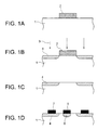
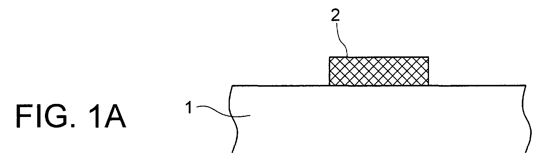
- the photovoltaic cell of the present invention is produced by the process shown in Figs. 1A to 1D.
- a highly viscous material containing silicon oxide is coated on a surface of p-type silicon semiconductor substrate 1 by a screen printing method in a pattern state, followed by firing to form a silicon oxide masking layer 2 (Fig. 1A).
- an n-type dopant layer 4 is formed on the portions having no masking layer 2 by gas phase diffusion using a gas 3 containing phosphorus which is a dopant showing n-type in silicon (Fig. 1B).
- the diffusion temperature is 870°C.
- the masking layer 2 is removed by using a hydrofluoric acid solution (Fig. 1C).
- an aluminum electrode 5 and a p-type dopant layer 6 are formed by coating aluminum in a pattern state using a screen printing method, followed by firing.
- a silver electrode 7 is formed by a screen printing method (Fig. 1D).
- the pn junction of the photovoltaic cell is constituted by the n-type dopant layer 4 and the p-type silicon semiconductor substrate 1. Further, even if the electroconductivity of the silicon semiconductor substrate 1 is n-type, the resulting product functions as a photovoltaic cell. In this case, the pn junction is constituted by the p-type dopant layer 6 and the n-type silicon semiconductor substrate.
- the masking layer 2 is formed by the screen printing method, but not limited thereto. There can be used other printing method such as an ink jet method, or the like. Further, by using a metal mask, the silicon oxide film can be deposited thereupon by plasma CVD, thermal CVD, or the like. In addition, the masking layer can be formed by using a silicon nitride (SiN x ) film, or the like.
- the masking layer 2 for the n-type dopant layer 4 and the silver electrode 7 are formed by the same method (the screen printing method), the tendency of deviation of pattern in the plane of semiconductor substrate 1 is the same. As a result, the generation percent of badness caused by misregistration can be reduced. This effect can also be seen in the following Examples taking the same constructing portion as this Example.
- a photovoltaic cell of this Example is produced by the process shown in Figs. 2A to 2C.
- a dopant layer 4 and a dopant layer 8 having the same electroconductivity and different dopant concentration profiles in the depth direction are formed on one surface of a semiconductor substrate 1.
- an n-type dopant layer 4 is formed in the same manner as described in Example 1 (Fig. 2A). Then, a masking layer 2 is removed by using a hydrofluoric acid solution, followed by diffusion of an n-type dopant at 830°C by gas phase diffusion using a gas 3 containing phosphorus which is a dopant showing n-type in silicon (Fig. 2B).
- n-type dopant layer 8 which has a different dopant concentration profile in the depth direction compared with the n-type dopant layer 4 and shallower in diffusion depth than the n-type dopant layer 4.
- the diffusion temperature (830°C) at the time of the formation of the n-type dopant layer 8 is lower than the diffusion temperature (870°C) at the time of formation of the n-type dopant layer 4.
- the influence of this gas phase diffution on the n-type dopant layer 4 previously formed is small.
- the photoelectric conversion efficiency can be enhanced.
- a silver electrode 7 for the n-type dopant layer 4 is formed by a screen printing method (Fig. 2C).
- a silver electrode is formed by a screen printing method on a rear side of the p-type semiconductor substrate 1 (not shown in the drawing).
- a photovoltaic cell of this Example is produced by the process shown in Figs. 3A to 3D.
- the masking layer 2 is also used as a solid phase diffusion source.
- a highly viscous material containing silicon oxide including boron which is a dopant showing p-type in silicon is coated by a screen printing method in pattern state, followed by firing to form a silicon oxide masking layer 2 (Fig. 3A).
- an n-type dopant layer 4 is formed by gas phase diffusion on the portion wherein no masking layer 2 is present.
- the diffusion temperature is 950°C.
- the masking layer 2 functions as a solid phase diffusion source and forms a p-type dopant layer 6 under the masking layer 2 at the same time (Fig. 3B).
- the masking layer 2 is removed by using a hydrofluoric acid solution (Fig. 3C).
- electrodes 5 and 7 made of silver are formed by using a screen printing method (Fig. 3D).
- the type of electroconductivity of dopant layers is different depending on the portions having the masking layer 2 or not (the p-type dopant layer 6 and the n-type dopant layer 4). But it is possible to make the type of electroconductivity the same, or to make the dopant concentration profile in the depth direction in the same electroconductivity different by properly selecting the type of electroconductivity and concentration of dopant contained in the masking layer 2 as a solid phase diffusion source, the type of electroconductivity and concentration of dopant in gas phase diffusion, treating temperature, treating atmosphere, and the like.
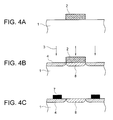
- Figs. 4A to 4C shows an example of producing a photovoltaic cell wherein the type of electroconductivity of a dopant layer formed by the gas phase diffusion and that of a dopant layer fomred by using the masking layer 2 as the solid phase diffusion source are made the same.
- an n-type dopant layer 4 is formed by gas phase diffusion and an n-type dopant layer 8 is formed by using the solid phase diffusion source at the same time.
- An electrode (not shown in the drawing) for p-type semiconductor substrate 1 is formed by using silver on a rear side of the p-type semiconductor substrate 1 by a screen printing method.
- a photovoltaic cell of this Example is produced by the process shown in Figs. 5A to 5D.
- This Example is fundamentally the same as Example 1.
- This Example is characterized by retaining the masking layer 2 finally, and opening the inside of masking layer to make a contact portion 19 of an electrode 5 and the semiconductor.
- the masking layer 2 is finally retained in the photovoltaic cell as in this Example, it is necessary to make the masking layer 2 from an electrically insulating substance.
- a highly viscous material containing silicon oxide is coated by a screen printing method so as to have an opening at the contact portion 19, followed by firing to form the masking layer 2 made of silicon oxide (Fig. 5A).
- an n-type dopant layer 4 is formed by gas phase diffusion on the portion wherein the masking layer 2 is not present (Fig. 5B).
- the diffusion temperature is 870°C.
- a p-type alloy layer is formed from aluminum and the semiconductor. This alloy layer penetrates the n-type dopant layer 4 to form a p-type dopant layer 6 by converting the n-type dopant layer 4 to the p-type (Fig. 5C).
- a silver electrode 7 is formed by a screen printing method (Fig. 5D).
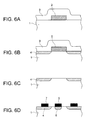
- a photovoltaic cell of this Example is produced by the process shown in Figs. 6A to 6D.
- solid phase diffusion is used in place of the gas phase diffusion used in Example 1.
- a silicon oxide solid phase diffusion source film 9 functioning as a solid phase diffusion source is formed on the whole surface of a p-type silicon semiconductor substrate 1 using a screen printing method.
- the solid phase diffusion source film 9 contains phosphorus therein which is a dopant showing n-type in silicon.
- an n-type dopant layer 4 is formed on the portion wherein the masking layer 2 is not present (Fig. 6B).
- the solid phase diffusion source film 9 and the masking layer 2 are removed by using a hydrofluoric acid solution (Fig. 6C).
- aluminum is coated in pattern state using a screen printing method, followed by firing to form an aluminum electrode 5 and a p-type dopant layer 6 under the electrode 5.
- a silver electrode 7 is formed by using a screen printing method (Fig. 6D).
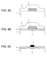
- photovoltaic cells having structures shown in Figs. 7D, 8C, 9D, and 10C can be produced by changing the type of electroconductivity of dopant contained in the solid phase diffusion source film 9, the concentration of dopant, the heat treatment temperature, the heat treatment time, the timing of the formation of solid phase diffusion source film 9 by the processes shown in Figs. 7A to 7D, 8A to 8C, 9A to 9D and 10A to 10C.
- a photovoltaic cell of this Example is produced by the process shown in Figs. 11A to 11D.
- a masking layer 2 is formed (Fig. 11A). Then, on the portion having no masking layer 2 of the surface of the p-type silicon substrate 1, an n-type dopant layer 4 is formed by converting the p-type dopant layer 6 by gas phase growth (Fig. 11B). In Figs. 11A to 11D, other conditions for production steps are the same as those of Example 1.
- an n-type dopant layer 4 can previously be formed on the whole surface of a p-type silicon semiconductor substrate 1, followed by conversion of the n-type dopant layer 4 under the masking layer 2 to a p-type dopant layer 6 by using the masking layer 2 also as a solid phase diffusion source.
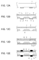
- a photovoltaic cell of this Example is produced by the process shown in Figs. 12A to 12E.
- a masking layer 2 having about 1 ⁇ m thickness is formed (Fig. 12A).
- n-type dopant layer 4 on the portions having no masking layer 2 (Fig. 12B).
- the n-type dopant layer 4 on the rear side functions as an n float.
- a silver electrode 7 for the n-type dopant layer 4 on the front surface and an aluminum electrode 5 for the p-type semiconductor substrate 1 are formed by using a screen printing method, while penetrating the antireflection coating film 16 and passivation film 15, respectively (Fig. 12E).
- Figs. 12A to 12E other conditions for production steps are the same as those in Example 1.
- a float-type photovoltaic cell of this Example is produced by the process shown in Figs. 13A to 13E.
- the steps are the same as those in Example 7 except for using the masking layer 2 as a solid phase diffusion source.
- a p-type dopant layer 6 is formed by solid phase diffusion.
- Conditions for producing the solid phase diffusion source are the same as those in Example 3.
- Other production conditions are the same as those in Example 1.
- the photovoltaic cell having high photoelectric conversion efficiency can be produced simply.
- a float-type photovolatic cell of this Example is produced by the process shown in Figs. 14A to 14D.
- This Example is characterized by retaining the masking layer 2 finally and opening the inside of the layer 2 to make a contact portion 19 of the electrode 5 and the semiconductor.
- a masking layer 2 having about 1 ⁇ m thickness and an opening at a contact portion 19 is formed (Fig. 14A).
- n-type dopant layer 4 on the portions having no masking layer 2 (Fig. 14B).
- the n-type dopant layer 4 on the rear side functions as an n float.
- thermal oxidation is conducted at 800°C to form an oxidation passivation film 15, on which a silicon nitride antireflection coating film 16 is formed by plasma CVD method (Fig. 14C).
- a silver electrode 7 for the n-type dopant layer 4 on the rear surface and an aluminum electrode 5 for the p-type semiconductor substrate 1 are formed by using a screen printing method, while penetrating the antireflection coating film 16 and passivation film 15, respectively.
- a p-type dopant layer 6 is formed under the electrode 5 (Fig. 14D).
- Figs. 14A to 14D other conditions for production steps are the same as those in Example 4.
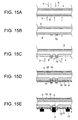
- a high-low junction type photovoltaic cell is produced by the process shown in Figs. 15A to 15E.
- This Example is characterized by retaining the masking layer 2 finally and opening the inside of the layer 2 to make a contact portion 19 of the electrode 5 and the semiconductor.
- a nitrogen gas containing BBr 3 as a p-type dopant diffusion gas 3 is blown on both surfaces of a p-type silicon semiconductor substrate 1 having resistivity of 3 ⁇ •cm at 950°C to form a p-type dopant layer 6 (Fig. 15A).
- a masking layer 2 having about 1 ⁇ m thickness and an opening at a contact portion 19 is formed (Fig. 15B).
- the portion of the rear side of the p-type silicon semiconductor substrate 1 having no masking layer 2 is subjected to conversion of the type of electroconductivity by gas phase diffusion only on the rear side by a back to back diffusion method to form an n-type dopant layer 4 (Fig. 15C).
- thermal oxidation is conducted at 800°C to form an oxidation passivation film 15, on which a titanium oxide (TiO 2 ) antireflection coating film 16 is formed by thermal CVD method (Fig. 15D).
- a silver electrode 10 for the n-type dopant layer 4 on the rear surface and an aluminum electrode 5 for the p-type dopant layer 6 are formed by using a screen printing method, while penetrating the antireflection coating film 16 and passivation film 15, respectively.
- the aluminum electrode 5 by firing the aluminum electrode 5 at 750°C, the dopant concentration of the p-type dopant layer 6 under the electrode 5 is increased (Fig. 15E).
- Figs. 15A to 15E other conditions for production steps are the same as those in Example 4.
- a photovoltaic cell of this Example is produced by the process shown in Figs. 16A to 16E.
- a through-hole 17 is made in, for example, a p-type silicon semiconductor substrate 1.
- the minority carrier generated on the front surface can be collected to the electrode 7 efficiently, resulting in producing the photovoltaic cell having high photoelectric conversion efficiency.
- a masking layer 2 containing boron is formed so as to partly cover the rear side of the through-hole of the p-type silicon semiconductor substrate 1 (Fig. 16A). Then, the boron in the masking layer 2 is diffused in the p-type silicon semiconductor substrate 1 by heat treatment at 900°C to form a p-type dopant layer 6 (Fig. 16B). Next, n-type dopant layers 4 are formed by gas phase diffusion on the portions other than the p-type dopant layer 6 of the p-type silicon semiconductor substrate 1 (Fig. 16C). After removing the masking layer 2, an oxide film 15 is formed by thermal oxidation (Fig. 16D).
- a silver electrode 7 for the n-type dopant layer 4 and a silver electrode 5 for the p-type semiconductor substrate 1 are formed through the oxide film 15 by a screen printing method (Fig. 16E).
- Other production conditions in Figs. 16A to 16E are the same as those in Example 3.
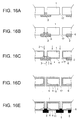
- Figs. 17A to 17F show concrete examples of the shape of masking layers 2 having openings used in the process for producing the photovoltaic cells of the present invention. Needless to say, the masking layers 2 of this Example can be used in Examples 4, 9 and 10.
- Figs. 17A, 17C, and 17E are plan views and Figs. 17B, 17D and 17F are cross-sectional views as taken on a dot and dash line of these plan views.
- the masking layer 2 shown at the left-hand side in Fig. 17A has an opening linearly.
- Fig. 17B by making the width of the electrode 5 narrower than that of the masking layer 2, even if the electrode 5 is shifted to right or left to some extent, it does not contact with the n-type dopant layer 4 formed outside of the masking layer 2.
- the width of precision is broadened to increase the yield of the production of the photovoltaic cells.
- the masking layer 2 shown at the right-hand side in Fig. 17A has an opening so as to have hole-like contact portion 19.
- the masking layer 2 shown in Fig. 17C has an opening in a doughnut shape. Since this shape can reduce the area of the contact portion 19 compared with the shapes of Fig. 17A, the photoelectric conversion efficiency can further be improved. Further, since the area of the n-type dopant layer 4 is also increased, the photoelectric conversion efficiency is also increase by this. As shown in Fig. 17D, it is necessary to connect each contact portion 19 by the electrode 15 in this shape, insulating layers 20 are inserted between the n-type dopant layer 4 and the electrode 5 to insulate both among individual contact portions 19.
- the masking layer 2 shown in Fig. 17E has a shape of a doughnut bonded by lines. In this shape, since the area of contact portion 19 can be reduced compared with the shape of Fig. 17A, the photoelectric conversion efficiency is further improved. In addition, since the area of the n-type dopant layer 4 increases, the photoelectric conversion efficiency is further increased by this. Moreover, comparing with the shape of Fig. 17C, since the insulating layer 20 is not necessary, the production steps can be simplified.
- the masking layer 2 can be formed by various methods as described in Example 1. For example, when the masking layer 2 is formed by a screen printing method, there appears a tendency specific to the coating method. When a shape shown in Fig. 18A is printed, the left-hand end of the pattern indicated by A portion takes the shape as shown in Fig. 18B (enlarged view), wherein there arise concave and convex between the most left end 21 and the most right end 22 with the width 25 of 10 ⁇ m or more. This is caused by precision of printing screen, deformation of the printing screen caused by stress at the time of printing, and further sag of printing material. Generally speaking, when a photolithography is used, the concave and convex is about 1 ⁇ m.
- the average position 24 of the left side shape shifts to the left with the length of numeral 26 compared with the position 23 on the design of the pattern of masking layer 2. This is caused by the shift of relative position with the printing screen and the semiconductor substrate 1 from the designed value.
- the shift is about 20 ⁇ m or more.
- the shift in the case of usual photolithography is about 1 ⁇ m.
- the difference in the width between the electrode 5 and the masking layer 2 should be larger than the total value of the concave and convex mentioned above and the shift of width. Further, by making the viscosity of the material for producing the masking layer 2 by screen printing method 50,000 to 1,000,000 cp, preferably 80,000 to 400,000 cp, it is possible to suppress blur and sag of the pattern.
- the concave and convex of pattern (width 31) and positional shift 32 as shown in Fig. 18C like Fig. 18B.
- Numerals 27, 28, 29 and 30 denote the most upper portion, the average position in the longitudinal direction, the most lower position, the position on design in the longitudinal direction, respectively. Therefore, in the design of pattern, shifts of these values should be taken into consideration.
- Examples 1 to 12 although explanation is omitted, it is possible to make a large number of concaves and convexes 14 as shown in Fig. 19 with the maximum height of about 10 ⁇ m on the surface of photovoltaic cells in order to reduce reflection of light. In this case, by enhancing the viscosity of the material for masking layer 2 for example, the top of concaves and convexes 14 can be covered with the masking layer 2.
- the electrode can be formed by a direct method for forming a pattern using a screen printing method, a photolithograhy method, or the like.
- the semiconductor substrate there can be used those obtained by using single crystals of silicon, germanium, galllium arsenic, or multi crystals of these elements and having an outer shape of circle, square, etc.
- the type of electroconductivity of the semiconductor substrate there can be used any types of i-type, p-type, and n-type.
- dopant layers and type of electroconductivity of semiconductor substrates are possible so long as photovoltaic cells can be formed.
- the dopant there can be used phosphorus, arsenic, antimony, boron, aluminum, gallium and the like conventionally used dopants.
Landscapes
- Photovoltaic Devices (AREA)
- Electrodes Of Semiconductors (AREA)
Abstract
A photovoltaic cell produced by adhering a
material for masking layer to a surface of a
semiconductor substrate in pattern state to form the
masking layer, and forming a dopant layer on the
portion having no masking layer by gas phase diffusion
or solid phase diffusion is high in photoelectric
conversion efficiency and is effective for preventing
lowering of minority carrier lifetime of the
semiconductor substrate.
Description
This invention relates to a photovoltaic cell
and a process for producing the same by using dopant
diffusion.
As photovoltaic cells produced by using
dopant diffusion, there are known, for example,
photovoltaic cells shown by Figs. 20A to 20F. The
photovoltaic cell shown in Fig. 20D is disclosed in
Fig. 1 (c) of Two Dimensional Study of Alternative Back
Surface Passivation Methods for High Efficiency Silicon
Solar Cells by M. Ghannam, et al (11th E.C.
Photovoltaic Solar Energy Conference, pp 45-48, 1992).
In Figs. 20A to 20F, numeral 1 denotes a p-type silicon
semiconductor substrate, numerals 4 and 8 denote n-type
dopant layers, numeral 6 denotes a p-type dopant layer,
and numerals 5, 7, and 10 denote electrodes.
A typical example for producing the known
photovoltaic cell of Fig. 20D is explained referring to
Figs. 21A to 21D. On surfaces of p-type silicon
semiconductor substrate 1, a SiO2 dopant (or impurity)
diffusion preventing films 11 are formed by using
thermal oxidation and photolithography and a p-type
dopant layer 6 is formed at an opening using a gas 3
containing a dopant which shows p-type in the silicon
(Fig. 21A). Then, the SiO2 dopant diffusion preventing
film 11 is removed and a SiO2 dopant diffusion
preventing film 12 is newly formed by using thermal
oxidation and photolithography, followed by formation
of n-type dopant layers 4 at the openings by gas phase
diffusion using a gas 3 containing a dopant which shows
n-typ in the silicon (Fig. 21B). Then, the dopant
diffusion preventing film 12 is removed (Fig. 21C).
Subsequently, silver electrodes 5 and 7 as electrodes
for the p-type dopant layer 6 and the n-type dopant
layer 4 are formed by a screen printing method (Fig.
21D).
In the above-mentioned production process,
since the semiconductor substrate 1 is exposed to high
temperatures by thermal oxidation during the formation
of two kinds of the SiO2 dopant diffusion preventing
films 11 and 12, a minority carrier lifetime of the
semiconductor substrate is lowered. This problem
arises not only in the photovoltaic cell of Fig. 20D
but also in the rest of photovoltaic cells shown in
Figs. 20A to 20F. Further, since the SiO2 dopant
diffusion preventing film 12 is formed on the p-type
dopant layer 6, the dopant in the p-type dopant layer 6
redistributes during the formation to change a dopant
concentration profile. This problem arises in the
photovoltaic cell of not only Fig. 20D but also Figs.
20C, 20 E and 20F, resulting in making the design of
photovoltaic cells difficult.
It is an object of the present invention to
provide photovoltaic cells preventing lowering of the
minority carrier lifetime of semiconductor substrates
and processes for producing the same.
The present invention provides a process for
producing a photovoltaic cell, which comprises
The present invention also provides a process
for producing a photovaltaic cell, which comprises
The present invention further provides a
photovoltaic cell comprising a semiconductor substrate,
an electrically insulating material layer formed on the
semiconductor substrate by a coating method, and
electrodes formed on openings of the electrically
insulating material layer.
The present invention still further provides
a photovoltaic cell comprising a semiconductor
substrate, and a dopant layer formed on the
semiconductor substrate and having different heights by
10 µm or more in periphery shape.
In order to prevent the lowering of minority
carrier lifetime of the semiconductor device, the
present inventors found that such an object can be
attained by adhering a material for a dopant diffusion
preventing mask (hereinafter referred to as "a masking
layer") to a surface of semiconductor substrate in
pattern state to form the masking layer and forming a
dopant layer on the portion wherein no masking layer is
present by gas phase diffusion or solid phase
diffusion. The adhesion of the material for the
masking layer can be carried out by a coating method
such as a printing method, e.g. a screen printing
method, an ink jet method, etc., a spraying method, a
chemical vapor deposition (CVD) method such as plasma
CVD, thermal CVD, etc.
The term "gas phase diffusion method" means a
diffusion method wherein atoms fly through a space and
reach the substrate, and includes an implantation
method, a plasma diffusion method, etc.
In the present invention, since the masking
layer, which functions as a mask at the time of forming
the dopant layer by the gas phase diffusion or solid
phase diffusion, is formed by adhering the material for
the masking layer in a pattern state to the substrate
not using the thermal oxidation method and the
photolithographic method, the semiconductor substrate
is not exposed to high temperatures. As a result,
lowering in the minority carrier lifetime can be
prevented.
The present invention includes the following
preferable embodiments.
The present invention is illustrated by way
of the following Examples, but needless to say, the
present invention is not limited to these Examples.
The photovoltaic cell of the present
invention is produced by the process shown in Figs. 1A
to 1D.
First, a highly viscous material containing
silicon oxide is coated on a surface of p-type silicon
semiconductor substrate 1 by a screen printing method
in a pattern state, followed by firing to form a
silicon oxide masking layer 2 (Fig. 1A).
Then, an n-type dopant layer 4 is formed on
the portions having no masking layer 2 by gas phase
diffusion using a gas 3 containing phosphorus which is
a dopant showing n-type in silicon (Fig. 1B). The
diffusion temperature is 870°C.
Then, the masking layer 2 is removed by using
a hydrofluoric acid solution (Fig. 1C).
Subsequently, an aluminum electrode 5 and a
p-type dopant layer 6 are formed by coating aluminum in
a pattern state using a screen printing method,
followed by firing. As an electrode for an n-type
dopant layer 4, a silver electrode 7 is formed by a
screen printing method (Fig. 1D).
In this Example, the pn junction of the
photovoltaic cell is constituted by the n-type dopant
layer 4 and the p-type silicon semiconductor substrate
1. Further, even if the electroconductivity of the
silicon semiconductor substrate 1 is n-type, the
resulting product functions as a photovoltaic cell. In
this case, the pn junction is constituted by the p-type
dopant layer 6 and the n-type silicon semiconductor
substrate.
As mentioned above, even if the electroconductivity
of semiconductor substrate is changed,
there can be obtained a structure which can function as
a photovoltaic cell. Such a structure will be
disclosed in the following Examples sometimes, but the
explanation is provided only to the use of p-type
silicon semiconductor substrate 1 for simplicity.
In this Example, the masking layer 2 is
formed by the screen printing method, but not limited
thereto. There can be used other printing method such
as an ink jet method, or the like. Further, by using a
metal mask, the silicon oxide film can be deposited
thereupon by plasma CVD, thermal CVD, or the like. In
addition, the masking layer can be formed by using a
silicon nitride (SiNx) film, or the like.
According to this Example, since the masking
layer 2 for the n-type dopant layer 4 and the silver
electrode 7 are formed by the same method (the screen
printing method), the tendency of deviation of pattern
in the plane of semiconductor substrate 1 is the same.
As a result, the generation percent of badness caused
by misregistration can be reduced. This effect can
also be seen in the following Examples taking the same
constructing portion as this Example.
A photovoltaic cell of this Example is
produced by the process shown in Figs. 2A to 2C. In
this Example, a dopant layer 4 and a dopant layer 8
having the same electroconductivity and different
dopant concentration profiles in the depth direction
are formed on one surface of a semiconductor substrate
1.
First, an n-type dopant layer 4 is formed in
the same manner as described in Example 1 (Fig. 2A).
Then, a masking layer 2 is removed by using a
hydrofluoric acid solution, followed by diffusion of an
n-type dopant at 830°C by gas phase diffusion using a
gas 3 containing phosphorus which is a dopant showing
n-type in silicon (Fig. 2B).
As a result, thre is formed on a portion from
which the masking layer 2 is removed an n-type dopant
layer 8, which has a different dopant concentration
profile in the depth direction compared with the n-type
dopant layer 4 and shallower in diffusion depth than
the n-type dopant layer 4. This is because the
diffusion temperature (830°C) at the time of the
formation of the n-type dopant layer 8 is lower than
the diffusion temperature (870°C) at the time of
formation of the n-type dopant layer 4. The influence
of this gas phase diffution on the n-type dopant layer
4 previously formed is small. As mentioned above, by
making the diffusion depth of the n-type dopant layer 8
which becomes a light receiving place shallow, the
photoelectric conversion efficiency can be enhanced.
Thereafter, a silver electrode 7 for the n-type
dopant layer 4 is formed by a screen printing
method (Fig. 2C). In the same manner, as an electrode
for the p-type semiconductor substrate 1, a silver
electrode is formed by a screen printing method on a
rear side of the p-type semiconductor substrate 1 (not
shown in the drawing).
A photovoltaic cell of this Example is
produced by the process shown in Figs. 3A to 3D. In
this Example, the masking layer 2 is also used as a
solid phase diffusion source.
First, on a surface of p-type silicon
semiconductor substrate 1, a highly viscous material
containing silicon oxide including boron which is a
dopant showing p-type in silicon is coated by a screen
printing method in pattern state, followed by firing to
form a silicon oxide masking layer 2 (Fig. 3A).
Then, using a gas 3 containing phosphorus
which is a dopant showing n-type in silicon, an n-type
dopant layer 4 is formed by gas phase diffusion on the
portion wherein no masking layer 2 is present. The
diffusion temperature is 950°C. At this time, the
masking layer 2 functions as a solid phase diffusion
source and forms a p-type dopant layer 6 under the
masking layer 2 at the same time (Fig. 3B).
Then, the masking layer 2 is removed by using
a hydrofluoric acid solution (Fig. 3C).
Subsequently, electrodes 5 and 7 made of
silver are formed by using a screen printing method
(Fig. 3D).
In the Example of Figs. 3A to 3D, the type of
electroconductivity of dopant layers is different
depending on the portions having the masking layer 2 or
not (the p-type dopant layer 6 and the n-type dopant
layer 4). But it is possible to make the type of
electroconductivity the same, or to make the dopant
concentration profile in the depth direction in the
same electroconductivity different by properly
selecting the type of electroconductivity and
concentration of dopant contained in the masking layer
2 as a solid phase diffusion source, the type of
electroconductivity and concentration of dopant in gas
phase diffusion, treating temperature, treating
atmosphere, and the like.
Figs. 4A to 4C shows an example of producing
a photovoltaic cell wherein the type of electroconductivity
of a dopant layer formed by the gas phase
diffusion and that of a dopant layer fomred by using
the masking layer 2 as the solid phase diffusion source
are made the same. As shown in Fig. 4B, an n-type
dopant layer 4 is formed by gas phase diffusion and an
n-type dopant layer 8 is formed by using the solid
phase diffusion source at the same time. An electrode
(not shown in the drawing) for p-type semiconductor
substrate 1 is formed by using silver on a rear
side of the p-type semiconductor substrate 1 by a
screen printing method.
A photovoltaic cell of this Example is
produced by the process shown in Figs. 5A to 5D. This
Example is fundamentally the same as Example 1. This
Example is characterized by retaining the masking layer
2 finally, and opening the inside of masking layer to
make a contact portion 19 of an electrode 5 and the
semiconductor. When the masking layer 2 is finally
retained in the photovoltaic cell as in this Example,
it is necessary to make the masking layer 2 from an
electrically insulating substance.
First, on a surface of p-type silicon
semiconductor substrate 1, a highly viscous material
containing silicon oxide is coated by a screen printing
method so as to have an opening at the contact portion
19, followed by firing to form the masking layer 2 made
of silicon oxide (Fig. 5A).
Then, using a gas 3 containing phosphorus as
a dopant showing n-type in silicon, an n-type dopant
layer 4 is formed by gas phase diffusion on the portion
wherein the masking layer 2 is not present (Fig. 5B).
The diffusion temperature is 870°C.
Subsequently, aluminum is coated in pattern
shape by a screen printing method, while retaining the
masking layer 2, followed by firing to form an aluminum
electrode 5. At this time, at the contact portion 19,
a p-type alloy layer is formed from aluminum and the
semiconductor. This alloy layer penetrates the n-type
dopant layer 4 to form a p-type dopant layer 6 by
converting the n-type dopant layer 4 to the p-type
(Fig. 5C). As an electrode for another n-type dopant
layer 4, a silver electrode 7 is formed by a screen
printing method (Fig. 5D).
In this Example, aluminum is used as a
material for electrode 5, but when a material for
electrode 5 containing antimony is used, it is possible
to form an n-type alloy layer. When a metal which
hardly forms an alloy layer with semiconductor is used
as a material for the electrode 5, it is possible to
form contact of the n-type dopant layer 4 and the
electrode 5 as shown in Fig. 5B. But even in this
case, it is possible to obtain direct contact with the
p-type silicon semiconductor substrate 1 by penetrating
the n-type dopant layer 4 when subjected to proper heat
treatment, or the like.
A photovoltaic cell of this Example is
produced by the process shown in Figs. 6A to 6D. In
this Example, solid phase diffusion is used in place of
the gas phase diffusion used in Example 1.
As shown in Fig. 6A, after forming a silicon
oxide masking layer 2, a silicon oxide solid phase
diffusion source film 9 functioning as a solid phase
diffusion source is formed on the whole surface of a p-type
silicon semiconductor substrate 1 using a screen
printing method. The solid phase diffusion source film
9 contains phosphorus therein which is a dopant showing
n-type in silicon.
After heat treating at 870°C, an n-type
dopant layer 4 is formed on the portion wherein the
masking layer 2 is not present (Fig. 6B).
Then, the solid phase diffusion source film 9
and the masking layer 2 are removed by using a
hydrofluoric acid solution (Fig. 6C). Subsequently,
aluminum is coated in pattern state using a screen
printing method, followed by firing to form an aluminum
electrode 5 and a p-type dopant layer 6 under the
electrode 5. Further, as an electrode for the n-type
dopant layer 4, a silver electrode 7 is formed by using
a screen printing method (Fig. 6D).
Based on the process of this Example,
photovoltaic cells having structures shown in Figs. 7D,
8C, 9D, and 10C can be produced by changing the type of
electroconductivity of dopant contained in the solid
phase diffusion source film 9, the concentration of
dopant, the heat treatment temperature, the heat
treatment time, the timing of the formation of solid
phase diffusion source film 9 by the processes shown in
Figs. 7A to 7D, 8A to 8C, 9A to 9D and 10A to 10C.
A photovoltaic cell of this Example is
produced by the process shown in Figs. 11A to 11D.
In this Example, after forming a p-type
dopant layer 6 by gas phase diffusion on the whole
surface of a p-type silicon semiconductor substrate 1,
a masking layer 2 is formed (Fig. 11A). Then, on the
portion having no masking layer 2 of the surface of the
p-type silicon substrate 1, an n-type dopant layer 4 is
formed by converting the p-type dopant layer 6 by gas
phase growth (Fig. 11B). In Figs. 11A to 11D, other
conditions for production steps are the same as those
of Example 1.
In the above process, an n-type dopant layer
4 can previously be formed on the whole surface of a p-type
silicon semiconductor substrate 1, followed by
conversion of the n-type dopant layer 4 under the
masking layer 2 to a p-type dopant layer 6 by using the
masking layer 2 also as a solid phase diffusion source.
A photovoltaic cell of this Example is
produced by the process shown in Figs. 12A to 12E.
First, on a rear side of a p-type silicon
semiconductor substrate 1 having resistivity of 3 Ω•cm,
a masking layer 2 having about 1 µm thickness is formed
(Fig. 12A).
Then, a nitrogen gas containing POCl3 is blown
on both surfaces of the p-type semiconductor substrate
1 at 870°C as a dopant diffusion gas 3 having n-type
electroconductivity to form an n-type dopant layer 4 on
the portions having no masking layer 2 (Fig. 12B). The
n-type dopant layer 4 on the rear side functions as an
n float.
Then, the masking layer 2 is removed (Fig.
12C). Subsequently, thermal oxidation is conducted at
800°C to form an oxidation passivation film 15, on
which a silicon nitride antireflection coating film 16
is formed by plasma CVD method (Fig. 12D).
Next, a silver electrode 7 for the n-type
dopant layer 4 on the front surface and an aluminum
electrode 5 for the p-type semiconductor substrate 1
are formed by using a screen printing method, while
penetrating the antireflection coating film 16 and
passivation film 15, respectively (Fig. 12E). In Figs.
12A to 12E, other conditions for production steps are
the same as those in Example 1.
A float-type photovoltaic cell of this
Example is produced by the process shown in Figs. 13A
to 13E. In this Example, the steps are the same as
those in Example 7 except for using the masking layer 2
as a solid phase diffusion source. At the time of
forming an n-type dopant layer 4 by gas phase
diffusion, a p-type dopant layer 6 is formed by solid
phase diffusion. Conditions for producing the solid
phase diffusion source are the same as those in Example
3. Other production conditions are the same as those
in Example 1.
Since good p-type dopant layer 6 can be
formed on a surface of the semiconductor substrate 1
under the electrode 5 at the rear side (Fig. 13E), the
photovoltaic cell having high photoelectric conversion
efficiency can be produced simply.
A float-type photovolatic cell of this
Example is produced by the process shown in Figs. 14A
to 14D. This Example is characterized by retaining the
masking layer 2 finally and opening the inside of the
layer 2 to make a contact portion 19 of the electrode 5
and the semiconductor.
First, on a rear side of a p-type silicon
semiconductor substrate 1 having resistivity of 3 Ω•cm,
a masking layer 2 having about 1 µm thickness and an
opening at a contact portion 19 is formed (Fig. 14A).
Then, a nitrogen gas containing POCl3 is blown
on both surfaces of the p-type semiconductor substrate
1 at 870°C as a dopant diffusion gas 3 having n-type
electroconductivity to form an n-type dopant layer 4 on
the portions having no masking layer 2 (Fig. 14B). The
n-type dopant layer 4 on the rear side functions as an
n float.
Then, while retaining the masking layer 2,
thermal oxidation is conducted at 800°C to form an
oxidation passivation film 15, on which a silicon
nitride antireflection coating film 16 is formed by
plasma CVD method (Fig. 14C).
Next, a silver electrode 7 for the n-type
dopant layer 4 on the rear surface and an aluminum
electrode 5 for the p-type semiconductor substrate 1
are formed by using a screen printing method, while
penetrating the antireflection coating film 16 and
passivation film 15, respectively. At this time, by
firing the aluminum electrode 5 at 750°C, a p-type
dopant layer 6 is formed under the electrode 5 (Fig.
14D). In Figs. 14A to 14D, other conditions for
production steps are the same as those in Example 4.
A high-low junction type photovoltaic cell is
produced by the process shown in Figs. 15A to 15E.
This Example is characterized by retaining the masking
layer 2 finally and opening the inside of the layer 2
to make a contact portion 19 of the electrode 5 and the
semiconductor.
First, a nitrogen gas containing BBr3 as a p-type
dopant diffusion gas 3 is blown on both surfaces
of a p-type silicon semiconductor substrate 1 having
resistivity of 3 Ω•cm at 950°C to form a p-type dopant
layer 6 (Fig. 15A).
Then, on rear side of the p-type silicon
semiconductor substrate 1, a masking layer 2 having
about 1 µm thickness and an opening at a contact
portion 19 is formed (Fig. 15B).
Next, the portion of the rear side of the p-type
silicon semiconductor substrate 1 having no
masking layer 2 is subjected to conversion of the type
of electroconductivity by gas phase diffusion only on
the rear side by a back to back diffusion method to
form an n-type dopant layer 4 (Fig. 15C).
Then, while retaining the masking layer 2,
thermal oxidation is conducted at 800°C to form an
oxidation passivation film 15, on which a titanium
oxide (TiO2) antireflection coating film 16 is formed by
thermal CVD method (Fig. 15D).
Next, a silver electrode 10 for the n-type
dopant layer 4 on the rear surface and an aluminum
electrode 5 for the p-type dopant layer 6 are formed by
using a screen printing method, while penetrating the
antireflection coating film 16 and passivation film 15,
respectively. At this time, by firing the aluminum
electrode 5 at 750°C, the dopant concentration of
the p-type dopant layer 6 under the electrode 5 is
increased (Fig. 15E). In Figs. 15A to 15E, other
conditions for production steps are the same as those
in Example 4.
A photovoltaic cell of this Example is
produced by the process shown in Figs. 16A to 16E. In
this Example, a through-hole 17 is made in, for
example, a p-type silicon semiconductor substrate 1.
In such a photovoltaic cell, since an n layer on the
front surface and an n layer on the rear surface are
connected by forming an n-type dopant layer 4 on the
front surface, rear surface and inside of the through-hole
17, the minority carrier generated on the front
surface can be collected to the electrode 7
efficiently, resulting in producing the photovoltaic
cell having high photoelectric conversion efficiency.
First, a masking layer 2 containing boron is
formed so as to partly cover the rear side of the
through-hole of the p-type silicon semiconductor
substrate 1 (Fig. 16A). Then, the boron in the masking
layer 2 is diffused in the p-type silicon semiconductor
substrate 1 by heat treatment at 900°C to form a p-type
dopant layer 6 (Fig. 16B). Next, n-type dopant layers
4 are formed by gas phase diffusion on the portions
other than the p-type dopant layer 6 of the p-type
silicon semiconductor substrate 1 (Fig. 16C). After
removing the masking layer 2, an oxide film 15 is
formed by thermal oxidation (Fig. 16D). Finally, a
silver electrode 7 for the n-type dopant layer 4 and a
silver electrode 5 for the p-type semiconductor
substrate 1 are formed through the oxide film 15 by a
screen printing method (Fig. 16E). Other production
conditions in Figs. 16A to 16E are the same as those in
Example 3.
Figs. 17A to 17F show concrete examples of
the shape of masking layers 2 having openings used in
the process for producing the photovoltaic cells of the
present invention. Needless to say, the masking layers
2 of this Example can be used in Examples 4, 9 and 10.
In the drawings, Figs. 17A, 17C, and 17E are plan views
and Figs. 17B, 17D and 17F are cross-sectional views as
taken on a dot and dash line of these plan views.
The masking layer 2 shown at the left-hand
side in Fig. 17A has an opening linearly. As shown in
Fig. 17B, by making the width of the electrode 5
narrower than that of the masking layer 2, even if the
electrode 5 is shifted to right or left to some extent,
it does not contact with the n-type dopant layer 4
formed outside of the masking layer 2. Thus, the width
of precision is broadened to increase the yield of the
production of the photovoltaic cells.
The masking layer 2 shown at the right-hand
side in Fig. 17A has an opening so as to have hole-like
contact portion 19. By making the area of contact
portion 19 between the electrode 5 and the p-type
semiconductor substrate small, recombination of
minority carrier at the interface between the electrode
5 and the semiconductor substrate 1 can be made small,
resulting in improving the photoelectric conversion
efficiency.
The masking layer 2 shown in Fig. 17C has an
opening in a doughnut shape. Since this shape can
reduce the area of the contact portion 19 compared with
the shapes of Fig. 17A, the photoelectric conversion
efficiency can further be improved. Further, since the
area of the n-type dopant layer 4 is also increased,
the photoelectric conversion efficiency is also
increase by this. As shown in Fig. 17D, it is
necessary to connect each contact portion 19 by the
electrode 15 in this shape, insulating layers 20 are
inserted between the n-type dopant layer 4 and the
electrode 5 to insulate both among individual contact
portions 19. In the case of a one-side light-receiving
type wherein the incident light enters from the
substrate side, when a white insulating material is
used as the insulating layer 20, the reflection
rate of the incident light at the insulating layer 20
increases and a light confinement ratio also increases.
The masking layer 2 shown in Fig. 17E has a
shape of a doughnut bonded by lines. In this shape,
since the area of contact portion 19 can be reduced
compared with the shape of Fig. 17A, the photoelectric
conversion efficiency is further improved. In
addition, since the area of the n-type dopant layer 4
increases, the photoelectric conversion efficiency is
further increased by this. Moreover, comparing with
the shape of Fig. 17C, since the insulating layer 20 is
not necessary, the production steps can be simplified.
The masking layer 2 can be formed by various
methods as described in Example 1. For example, when
the masking layer 2 is formed by a screen printing
method, there appears a tendency specific to the
coating method. When a shape shown in Fig. 18A is
printed, the left-hand end of the pattern indicated by
A portion takes the shape as shown in Fig. 18B
(enlarged view), wherein there arise concave and convex
between the most left end 21 and the most right end 22
with the width 25 of 10 µm or more. This is caused by
precision of printing screen, deformation of the
printing screen caused by stress at the time of
printing, and further sag of printing material.
Generally speaking, when a photolithography is used,
the concave and convex is about 1 µm. Further, the
average position 24 of the left side shape shifts to
the left with the length of numeral 26 compared with
the position 23 on the design of the pattern of masking
layer 2. This is caused by the shift of relative
position with the printing screen and the semiconductor
substrate 1 from the designed value. In a usual screen
printing method, the shift is about 20 µm or more. The
shift in the case of usual photolithography is about 1
µm.
As explained above using Figs. 17A and 17B,
the difference in the width between the electrode 5 and
the masking layer 2 should be larger than the total
value of the concave and convex mentioned above and the
shift of width. Further, by making the viscosity of
the material for producing the masking layer 2 by
screen printing method 50,000 to 1,000,000 cp,
preferably 80,000 to 400,000 cp, it is possible to
suppress blur and sag of the pattern. In addition, as
to the B portion of the upper portion of pattern shown
in Fig. 18A, there also arise the concave and convex of
pattern (width 31) and positional shift 32 as shown in
Fig. 18C like Fig. 18B. Numerals 27, 28, 29 and 30
denote the most upper portion, the average position in
the longitudinal direction, the most lower position,
the position on design in the longitudinal direction,
respectively. Therefore, in the design of pattern,
shifts of these values should be taken into
consideration.
In Examples 1 to 12, although explanation is
omitted, it is possible to make a large number of
concaves and convexes 14 as shown in Fig. 19 with the
maximum height of about 10 µm on the surface of
photovoltaic cells in order to reduce reflection of
light. In this case, by enhancing the viscosity of the
material for masking layer 2 for example, the top of
concaves and convexes 14 can be covered with the
masking layer 2.
The electrode can be formed by a direct
method for forming a pattern using a screen printing
method, a photolithograhy method, or the like.
As the semiconductor substrate, there can be
used those obtained by using single crystals of
silicon, germanium, galllium arsenic, or multi crystals
of these elements and having an outer shape of circle,
square, etc. As the type of electroconductivity of the
semiconductor substrate, there can be used any types of
i-type, p-type, and n-type. Various combinations of
dopant layers and type of electroconductivity of
semiconductor substrates are possible so long as photovoltaic
cells can be formed. As the dopant, there can
be used phosphorus, arsenic, antimony, boron, aluminum,
gallium and the like conventionally used dopants.
Claims (18)
- A process for producing a photovoltaic cell, which comprisesa step of forming a dopant diffusion preventing mask on a surface of a semiconductor substrate by adhering a material for the dopant diffusion preventing mask in a pattern state to the semiconductor substrate surface, anda step of forming a first dopant layer on a portion not covered by the dopant diffusion preventing mask by a first gas phase diffusion.
- A process according to claim 1, which further comprisesa step of removing the dopant diffusion preventing mask after the first dopant layer forming step, anda step of forming a second dopant layer by a second gas phase diffusion on the region from which the dopant diffusion preventing mask is removed.
- A process according to claim 1, wherein the dopant diffusion preventing mask contains a dopant so as to function as a solid phase diffusion source, and a third dopant layer is formed under the dopant diffusion preventing mask.
- A process according to claim 1, wherein the semiconductor substrate is made of silicon, the dopant diffusion preventing mask is made of an electrically insulating material and has an opening, said process further comprises after the step of forming the first dopant layera step of coating a metal containing a dopant which decides a type of electroconductivity in the opening in the dopant diffusion preventing mask,a step of converting the first dopant layer to a dopant layer having an opposite electroconductivity by firing, anda step of forming a metallic electrode for the impurity layer having the opposite electroconductivity.
- A process according to claim 1, wherein the semiconductor substrate is made of silicon, the dopant diffusion preventing mask is made of an electrically insulating material and has an opening, said process further comprises after the step of forming the first dopant layera step of coating aluminum containing a dopant which decides a type of electroconductivity in the opening in the dopant diffusion preventing mask,a step of converting the first dopant layer to a p-type dopant layer by firing, anda step of forming an aluminum electrode for the p-type dopant layer.
- A process according to claim 1, wherein a dopant layer having an opposite electroconductivity to the first dopant layer is formed before the step of formation of the dopant diffusion preventing mask.
- A process according to claim 1, wherein the semiconductor substrate has a through-hole which penetrates from a front surface to a rear surface and said process comprisinga step of forming the first dopant layer on the front surface and rear surface of the semiconductor substrate having no dopant diffusion preventing mask and inside wall of the through-hole by the first gas phase diffusion.
- A process for producing a photovaltaic cell, which comprisesa step of forming a dopant diffusion preventing mask on a surface of a semiconductor substrate by adhering a material for the dopant diffusion preventing mask in a pattern state to the semiconductor substrate surface,a step of forming a solid phase diffusion source layer, anda step of forming a first dopant layer on the portion having no dopant diffusion preventing mask by solid phase diffusion from the solid phase diffusion source layer.
- A process according to claim 8, wherein the dopant diffusion preventing mask contains a dopant so as to function as a solid phase diffusion source, and a second dopant layer is formed under the dopant diffusion preventing mask.
- A process according to claim 1 or 8, wherein the material for the dopant diffusion preventing mask is adhered to the semiconductor substrate by a printing method.
- A process according to claim 1 or 8, wherein the material for the dopant diffusion preventing mask contains silicon oxide or silicon nitride.
- A process according to claim 1, wherein the material for the dopant diffusion preventing mask has a viscosity of 500,000 cp to 1,000,000 cp.
- A process according to claim 8, wherein the material for the dopant diffusion preventing mask and a material for the solid phase diffusion source layer have a viscosity of 500,000 cp to 1,000,000 cp.
- A photovoltaic cell comprising a semiconductor substrate, an electrically insulating material layer formed on the semiconductor substrate by a coating method, and electrodes formed on openings of the electrically insulating material layer.
- A photovoltaic cell according to claim 14, which further comprises a first dopant layer formed on outside of the electrically insulating material layer on the semiconductor substrate, and a second dopant layer having an opposite electroconductivity to the first dopant layer and formed in the opening of the electrically insulating material layer, said second dopant layer containing p-type dopant and n-type dopant.
- A photovoltaic cell according to claim 15, wherein the fist dopant layer is an n-type dopant layer, the second dopant layer is a p-type dopant layer, the semiconductor substate is made of silicon, the electrode is made of aluminum, and said p-type dopant layer contains aluminum and an n-type dopant.
- A photovoltaic cell comprising a semiconductor substrate, and a dopant layer formed on the semiconductor substrate and having different heights by 10 µm or more in periphery shape.
- A photovoltaic cell according to claim 17, which further comprises a through-hole penetrating the semiconductor substrate from a front surface to a rear surface, and a dopant layer having the same electroconductivity and connecting the front surface, the rear surface and inside of through-hole.
Applications Claiming Priority (2)
| Application Number | Priority Date | Filing Date | Title |
|---|---|---|---|
| JP2000318236 | 2000-10-13 | ||
| JP2000318236A JP2002124692A (en) | 2000-10-13 | 2000-10-13 | Solar cell and method of manufacturing the same |
Publications (1)
| Publication Number | Publication Date |
|---|---|
| EP1199754A2 true EP1199754A2 (en) | 2002-04-24 |
Family
ID=18796890
Family Applications (1)
| Application Number | Title | Priority Date | Filing Date |
|---|---|---|---|
| EP01106171A Withdrawn EP1199754A2 (en) | 2000-10-13 | 2001-03-13 | Photovoltaic cell and process for producing the same |
Country Status (3)
| Country | Link |
|---|---|
| US (1) | US20020046765A1 (en) |
| EP (1) | EP1199754A2 (en) |
| JP (1) | JP2002124692A (en) |
Cited By (3)
| Publication number | Priority date | Publication date | Assignee | Title |
|---|---|---|---|---|
| EP1763086A1 (en) * | 2005-09-09 | 2007-03-14 | Interuniversitair Micro-Elektronica Centrum | Photovoltaic cell with thick silicon oxide and silicon nitride passivation and fabrication method |
| EP2164113A1 (en) * | 2008-09-16 | 2010-03-17 | Gintech Energy Corporation | One-step diffusion method for fabricating a differential doped solar cell |
| WO2019091112A1 (en) * | 2017-11-10 | 2019-05-16 | 常州亿晶光电科技有限公司 | Preparation process without etching treatment for solar cell |
Families Citing this family (31)
| Publication number | Priority date | Publication date | Assignee | Title |
|---|---|---|---|---|
| US20060060238A1 (en) * | 2004-02-05 | 2006-03-23 | Advent Solar, Inc. | Process and fabrication methods for emitter wrap through back contact solar cells |
| JP4481869B2 (en) * | 2005-04-26 | 2010-06-16 | 信越半導体株式会社 | SOLAR CELL MANUFACTURING METHOD, SOLAR CELL, AND SEMICONDUCTOR DEVICE MANUFACTURING METHOD |
| JP2006310368A (en) * | 2005-04-26 | 2006-11-09 | Shin Etsu Handotai Co Ltd | Solar cell manufacturing method and solar cell |
| US7846823B2 (en) | 2005-08-12 | 2010-12-07 | Sharp Kabushiki Kaisha | Masking paste, method of manufacturing same, and method of manufacturing solar cell using masking paste |
| JP5283824B2 (en) * | 2006-01-18 | 2013-09-04 | 東京応化工業株式会社 | Film-forming composition |
| US8008575B2 (en) * | 2006-07-24 | 2011-08-30 | Sunpower Corporation | Solar cell with reduced base diffusion area |
| JP2008186927A (en) * | 2007-01-29 | 2008-08-14 | Sharp Corp | Back junction solar cell and manufacturing method thereof |
| JP5236914B2 (en) * | 2007-09-19 | 2013-07-17 | シャープ株式会社 | Manufacturing method of solar cell |
| KR20100135276A (en) * | 2008-03-26 | 2010-12-24 | 메르크 파텐트 게엠베하 | SIO 2 resist layer composition composition and its use method |
| US20090283145A1 (en) * | 2008-05-13 | 2009-11-19 | Kim Yun-Gi | Semiconductor Solar Cells Having Front Surface Electrodes |
| US20100035422A1 (en) * | 2008-08-06 | 2010-02-11 | Honeywell International, Inc. | Methods for forming doped regions in a semiconductor material |
| US8053867B2 (en) * | 2008-08-20 | 2011-11-08 | Honeywell International Inc. | Phosphorous-comprising dopants and methods for forming phosphorous-doped regions in semiconductor substrates using phosphorous-comprising dopants |
| US7951696B2 (en) * | 2008-09-30 | 2011-05-31 | Honeywell International Inc. | Methods for simultaneously forming N-type and P-type doped regions using non-contact printing processes |
| US8518170B2 (en) * | 2008-12-29 | 2013-08-27 | Honeywell International Inc. | Boron-comprising inks for forming boron-doped regions in semiconductor substrates using non-contact printing processes and methods for fabricating such boron-comprising inks |
| DE102009005168A1 (en) * | 2009-01-14 | 2010-07-22 | Fraunhofer-Gesellschaft zur Förderung der angewandten Forschung e.V. | Solar cell and method for producing a solar cell from a silicon substrate |
| JP2010205839A (en) * | 2009-03-02 | 2010-09-16 | Sharp Corp | Method of manufacturing semiconductor device |
| US8288645B2 (en) * | 2009-03-17 | 2012-10-16 | Sharp Laboratories Of America, Inc. | Single heterojunction back contact solar cell |
| US8324089B2 (en) * | 2009-07-23 | 2012-12-04 | Honeywell International Inc. | Compositions for forming doped regions in semiconductor substrates, methods for fabricating such compositions, and methods for forming doped regions using such compositions |
| WO2011017659A1 (en) * | 2009-08-06 | 2011-02-10 | Energy Focus, Inc. | Method of passivating and reducing reflectance of a photovoltaic cell |
| JP2011119341A (en) * | 2009-12-01 | 2011-06-16 | Sharp Corp | Method of forming diffusion-preventive mask, and method of manufacturing solar cell using the same |
| MY166305A (en) * | 2009-12-09 | 2018-06-25 | Solexel Inc | High-efficiency photovoltaic back-contact solar cell structures and manufacturing methods using thin planar semiconductor absorbers |
| KR101699313B1 (en) * | 2010-10-05 | 2017-02-13 | 엘지전자 주식회사 | Method for manufacturing solar cell |
| US8586403B2 (en) | 2011-02-15 | 2013-11-19 | Sunpower Corporation | Process and structures for fabrication of solar cells with laser ablation steps to form contact holes |
| US8629294B2 (en) | 2011-08-25 | 2014-01-14 | Honeywell International Inc. | Borate esters, boron-comprising dopants, and methods of fabricating boron-comprising dopants |
| US8975170B2 (en) | 2011-10-24 | 2015-03-10 | Honeywell International Inc. | Dopant ink compositions for forming doped regions in semiconductor substrates, and methods for fabricating dopant ink compositions |
| US20130306130A1 (en) * | 2012-05-21 | 2013-11-21 | Stion Corporation | Solar module apparatus with edge reflection enhancement and method of making the same |
| JP5905966B2 (en) * | 2012-08-09 | 2016-04-20 | 三菱電機株式会社 | Manufacturing method of solar cell |
| CN103746039A (en) * | 2014-01-09 | 2014-04-23 | 东莞南玻光伏科技有限公司 | Back passivation method of crystalline silicon solar cell and preparation method of crystalline silicon solar cell |
| JP2015211117A (en) * | 2014-04-25 | 2015-11-24 | 三菱電機株式会社 | Method of manufacturing solar cell and solar cell |
| KR102325522B1 (en) * | 2015-01-29 | 2021-11-12 | 엘지전자 주식회사 | Method for manufacturing metal chalcogenide film |
| EP3404724B1 (en) * | 2017-05-19 | 2022-08-03 | LG Electronics Inc. | Solar cell and method for manufacturing the same |
-
2000
- 2000-10-13 JP JP2000318236A patent/JP2002124692A/en active Pending
-
2001
- 2001-03-13 EP EP01106171A patent/EP1199754A2/en not_active Withdrawn
- 2001-03-20 US US09/811,407 patent/US20020046765A1/en not_active Abandoned
Cited By (4)
| Publication number | Priority date | Publication date | Assignee | Title |
|---|---|---|---|---|
| EP1763086A1 (en) * | 2005-09-09 | 2007-03-14 | Interuniversitair Micro-Elektronica Centrum | Photovoltaic cell with thick silicon oxide and silicon nitride passivation and fabrication method |
| EP2164113A1 (en) * | 2008-09-16 | 2010-03-17 | Gintech Energy Corporation | One-step diffusion method for fabricating a differential doped solar cell |
| US7867809B2 (en) | 2008-09-16 | 2011-01-11 | Gintech Energy Corporation | One-step diffusion method for fabricating a differential doped solar cell |
| WO2019091112A1 (en) * | 2017-11-10 | 2019-05-16 | 常州亿晶光电科技有限公司 | Preparation process without etching treatment for solar cell |
Also Published As
| Publication number | Publication date |
|---|---|
| US20020046765A1 (en) | 2002-04-25 |
| JP2002124692A (en) | 2002-04-26 |
Similar Documents
| Publication | Publication Date | Title |
|---|---|---|
| EP1199754A2 (en) | Photovoltaic cell and process for producing the same | |
| US5258077A (en) | High efficiency silicon solar cells and method of fabrication | |
| AU2006237110B2 (en) | Rear contact solar cell and method for making same | |
| EP1449261B1 (en) | SOLAR CELL WITH BACKSIDE CONTACTS and its manufacturing method | |
| US20110253211A1 (en) | Solar cell and method for manufacturing same | |
| US20110000530A1 (en) | Method of fabrication of a back-contacted photovoltaic cell, and back-contacted photovoltaic cell made by such a method | |
| CN119008722A (en) | Interdigital back contact type solar cell with p-type conductivity | |
| EP2086015A2 (en) | Solar Cell and Method for Manufacturing the same | |
| JP2007184580A (en) | Solar cell and manufacturing method thereof | |
| KR19990063990A (en) | Self-Regulating (SALDE) Solar Cells with Partially Deeply Dispersed Emitters and Methods of Manufacturing the Same | |
| JPH10233518A (en) | Method of manufacturing solar cell, method of manufacturing solar cell and semiconductor device | |
| EP2581942A1 (en) | Solar cell | |
| US20170194519A1 (en) | Solar cell element | |
| US20090050202A1 (en) | Solar cell and method for forming the same | |
| TW202404111A (en) | Back-contact solar cells with passivated contacts and methods of making them | |
| JP2003209271A (en) | Solar cell and method of manufacturing the same | |
| JP2013187462A (en) | Photoelectric conversion element and method for manufacturing the same | |
| KR101093114B1 (en) | Solar cell with back junction structure | |
| KR20050098472A (en) | Solar cell and fabrication method thereof | |
| JP3368145B2 (en) | Method of manufacturing solar cell | |
| KR101321538B1 (en) | Bulk silicon solar cell and method for producing same | |
| JPH11135812A (en) | Method of forming solar cell element | |
| JPH08274356A (en) | Solar cell element | |
| JP2005167291A (en) | Method for manufacturing solar cell and method for manufacturing semiconductor device | |
| JP2006295212A (en) | Method for manufacturing solar cell and method for manufacturing semiconductor device |
Legal Events
| Date | Code | Title | Description |
|---|---|---|---|
| PUAI | Public reference made under article 153(3) epc to a published international application that has entered the european phase |
Free format text: ORIGINAL CODE: 0009012 |
|
| AK | Designated contracting states |
Kind code of ref document: A2 Designated state(s): AT BE CH CY DE DK ES FI FR GB GR IE IT LI LU MC NL PT SE TR |
|
| AX | Request for extension of the european patent |
Free format text: AL;LT;LV;MK;RO;SI |
|
| STAA | Information on the status of an ep patent application or granted ep patent |
Free format text: STATUS: THE APPLICATION HAS BEEN WITHDRAWN |
|
| 18W | Application withdrawn |
Effective date: 20030623 |