EP1198011A1 - Semiconductor device including mos field-effect transistor - Google Patents
Semiconductor device including mos field-effect transistor Download PDFInfo
- Publication number
- EP1198011A1 EP1198011A1 EP00946307A EP00946307A EP1198011A1 EP 1198011 A1 EP1198011 A1 EP 1198011A1 EP 00946307 A EP00946307 A EP 00946307A EP 00946307 A EP00946307 A EP 00946307A EP 1198011 A1 EP1198011 A1 EP 1198011A1
- Authority
- EP
- European Patent Office
- Prior art keywords
- conductivity type
- regions
- source electrode
- region
- source
- Prior art date
- Legal status (The legal status is an assumption and is not a legal conclusion. Google has not performed a legal analysis and makes no representation as to the accuracy of the status listed.)
- Withdrawn
Links
Images


Classifications
-
- H—ELECTRICITY
- H10—SEMICONDUCTOR DEVICES; ELECTRIC SOLID-STATE DEVICES NOT OTHERWISE PROVIDED FOR
- H10D—INORGANIC ELECTRIC SEMICONDUCTOR DEVICES
- H10D84/00—Integrated devices formed in or on semiconductor substrates that comprise only semiconducting layers, e.g. on Si wafers or on GaAs-on-Si wafers
- H10D84/101—Integrated devices comprising main components and built-in components, e.g. IGBT having built-in freewheel diode
- H10D84/141—VDMOS having built-in components
- H10D84/143—VDMOS having built-in components the built-in components being PN junction diodes
- H10D84/144—VDMOS having built-in components the built-in components being PN junction diodes in antiparallel diode configurations
-
- H—ELECTRICITY
- H10—SEMICONDUCTOR DEVICES; ELECTRIC SOLID-STATE DEVICES NOT OTHERWISE PROVIDED FOR
- H10D—INORGANIC ELECTRIC SEMICONDUCTOR DEVICES
- H10D30/00—Field-effect transistors [FET]
- H10D30/60—Insulated-gate field-effect transistors [IGFET]
- H10D30/64—Double-diffused metal-oxide semiconductor [DMOS] FETs
- H10D30/66—Vertical DMOS [VDMOS] FETs
- H10D30/665—Vertical DMOS [VDMOS] FETs having edge termination structures
-
- H—ELECTRICITY
- H10—SEMICONDUCTOR DEVICES; ELECTRIC SOLID-STATE DEVICES NOT OTHERWISE PROVIDED FOR
- H10D—INORGANIC ELECTRIC SEMICONDUCTOR DEVICES
- H10D62/00—Semiconductor bodies, or regions thereof, of devices having potential barriers
- H10D62/10—Shapes, relative sizes or dispositions of the regions of the semiconductor bodies; Shapes of the semiconductor bodies
- H10D62/124—Shapes, relative sizes or dispositions of the regions of semiconductor bodies or of junctions between the regions
- H10D62/126—Top-view geometrical layouts of the regions or the junctions
- H10D62/127—Top-view geometrical layouts of the regions or the junctions of cellular field-effect devices, e.g. multicellular DMOS transistors or IGBTs
-
- H—ELECTRICITY
- H10—SEMICONDUCTOR DEVICES; ELECTRIC SOLID-STATE DEVICES NOT OTHERWISE PROVIDED FOR
- H10D—INORGANIC ELECTRIC SEMICONDUCTOR DEVICES
- H10D84/00—Integrated devices formed in or on semiconductor substrates that comprise only semiconducting layers, e.g. on Si wafers or on GaAs-on-Si wafers
- H10D84/101—Integrated devices comprising main components and built-in components, e.g. IGBT having built-in freewheel diode
- H10D84/141—VDMOS having built-in components
- H10D84/146—VDMOS having built-in components the built-in components being Schottky barrier diodes
-
- H—ELECTRICITY
- H10—SEMICONDUCTOR DEVICES; ELECTRIC SOLID-STATE DEVICES NOT OTHERWISE PROVIDED FOR
- H10D—INORGANIC ELECTRIC SEMICONDUCTOR DEVICES
- H10D62/00—Semiconductor bodies, or regions thereof, of devices having potential barriers
- H10D62/10—Shapes, relative sizes or dispositions of the regions of the semiconductor bodies; Shapes of the semiconductor bodies
- H10D62/17—Semiconductor regions connected to electrodes not carrying current to be rectified, amplified or switched, e.g. channel regions
- H10D62/393—Body regions of DMOS transistors or IGBTs
Definitions
- the present invention relates to a semiconductor device having a MOS field-effect transistor (hereinafter abbreviated as MOSFET) such as a vertical-type power MOSFET or a double diffusion-type MOSFET. More particularly, the present invention relates to such a MOSFET that has a very short turn-ON/OFF time and an improved reverse withstanding voltage.
- MOSFET MOS field-effect transistor
- a driver circuit is frequently used which employs a vertical-type or double diffusion-type power MOSFET to drive an inductive load such as a motor.
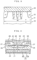
- the vertical-type power MOSFET has such a configuration, as shown in FIG. 4, that a P-well 21 is formed on the surface of an N-type semiconductor layer 20 provided on a N + -type semiconductor substrate 20a, and at an outer periphery of this P-well 21 is formed a ring-shaped N + -type source diffusion layer 22.
- the semiconductor layer 20 outside the P-well 21 and the semiconductor substrate 20a act as a drain layer 23.
- the surface region of the P-well 21 between the drain layer 23 and the source layer 22 acts as a channel region 26, on which is provided a gate electrode 28 with a gate insulator film 27 interposed therebetween.
- a P + -type region 25 for ohmic-contact is provided at the center of the P-well 21 at the center of the P-well 21 at the center of the P-well 21 .
- the drain electrode 24 is provided on the back surface of the semiconductor substrate 20a.
- the vertical-type MOSFET is formed.
- a PN junction of the P-well 21 and the N-type semiconductor layer 20 forms a so-called built-in diode (body diode).
- This built-in diode is structured so as to be connected in the reverse direction between the drain and the source and can be used as a flywheel diode for inducing a reverse recovery current ascribed to a counter electromotive force of an inductive load.
- the counter electromotive force of the inductive load acts to apply a voltage in the forward direction on the built-in diode, which is accompanied, as well known, by accumulation of minority carrier, that is, electrons in the P-well.
- accumulated minority carrier inhibits rapid interruption of the operation of the built-in diode at the time of rectification when the current is changed in flow direction.
- the flow of this minority carrier is concentrated to part of the device, the PN junction portion of the P-well and the drain layer is broken and hence the power MOSFET is broken eventually.
- a semiconductor device including a MOS field-effect transistor according to the present invention includes; a MOS field-effect transistor; and a diode which is built in the transistor and connected between a source electrode and a drain electrode thereof so that when a voltage in the reverse direction is applied between the source electrode and the drain electrode at the time of operation, which forms a current path between the source electrode and the drain electrode, wherein a contact portion of the diode with the source electrode has such a construction that a high-impurity concentration region having a second conductivity type which is a conductivity type of the source electrode side semiconductor layer of the diode, and a region having a first conductivity type opposite to the conductivity type or a low-impurity concentration region having the second conductivity type are formed alternately in a plan structure.
- the "high-impurity concentration" of the high-impurity concentration region of the second conductivity type means such an impurity concentration as to form an ohmic contact with the source electrode.
- the MOS field-effect transistor is a double-diffusion type MOS field-effect transistor that has a first conductivity type semiconductor layer which provides a drain region, second conductivity type regions which are formed by diffusion in the first conductivity type semiconductor layer, and source regions having a first conductivity type formed by diffusion at an outer periphery of each of the second conductivity type regions in such a configuration that such portions of the second conductivity type regions which are positioned between each of the source regions and the drain region act as channel regions.
- the source electrode is provided so as to be in contact with each of the source regions and a surface portion of each of the second conductivity type regions opposite to each of the channel regions with respect to each of the source regions.
- the second conductivity type regions are formed in a matrix in the first conductivity type semiconductor layer
- each of the source regions is formed in a ring shape on a plan view in each of the second conductivity type regions so as to give a constant gap at the periphery of each of the second conductivity type regions
- the source electrode is formed at a predetermined region of an inner circumference of each of the ring-shaped source regions and the entire inner surface of each of the second conductivity type regions, thus providing a mass-capacity power MOSFET.
- the contact portion has such a construction that a contact portion of each of the second conductivity type regions with the source electrode has such a construction that one or more first conductivity type high impurity-concentration regions each of which is ring shape on a plan view and one or more second conductivity type high impurity-concentration regions are provided alternately or that the second conductivity type regions have a low impurity concentration; and wherein a contact portion of each of the second conductivity type regions with the source electrode has such a construction that second conductivity type high impurity-concentration regions are evenly spaced in each of the second conductivity type regions.
- a semiconductor device having a MOSFET according to the present invention with reference to the drawings.
- a semiconductor device having a MOSFET of the present invention in a surface of the N-type semiconductor layer 20 is formed a predetermined pattern of a P-wells 21 by diffusion.
- a large-area P-well 21a P-well below the pad
- each of P-wells 21 is, for example, rectangular in a plan view.
- each of the P-wells 21 is formed, for example, a rectangular ring-shaped N + -type diffused source region 22.
- the semiconductor layer 20 except this P-well 21 and an N + -type semiconductor substrate 20a on which this semiconductor layer 20 is grown act as a drain region 23, thus providing a vertical-type double-diffusion MOSFET.
- a drain electrode 24 On the back side surface of the N + -type semiconductor substrate 20a is provided a drain electrode 24.
- a surface layer portion positioned between the drain region 23 and the diffused source region 22 provides a channel region 26 in which is formed a channel 50 when the MOSFET is turned ON.
- a gate electrode 28 with a gate insulator film 27 interposed therebetween is formed above this channel region 26 .
- the gate electrode 28 directly below the gate pad 36 is connected to the gate pad 36 through a contact hole 30 formed in the insulator film 29 on the gate electrode 28.
- the other gate electrodes 28 are connected to the gate electrodes 28 directly below the gate pad 36 at a position not shown in the figure.
- a source electrode 33 formed on the insulator film 29 is commonly connected through this source contact holes 31 to all of the diffused source region 22 provided on the surface of each P-well 21 and the surfaces of portions surrounded by the diffused source region 22 in each P-well 21.
- a contact portion 40 of the p-well 21 with the source electrode 33 is not formed of a contact region only of a p + -type region but is formed in such a configuration that a P + -type region and an N + -type region alternate with each other in a plan view.
- FIG. 2A illustrating a plan view of the contact portion 40 with the source electrode 33 etc. as removed and FIG. 2B illustrating an expanded cross-sectional view of part of FIG. 2A
- in the outer surface layer of such a region of the P-well 21 that is surrounded by the rectangular ring-shaped diffused source region 22 are formed concentrically a small-width N + -type (or N-type) ring-shaped region 41 and an equivalently small-width P + -type ring-shaped region 42 alternately.
- These regions 41 and 42 make up the contact portion 40 and all come in contact with the source electrode 33 in an ohmic manner. That is, the N + -type region 41 and the P + -type region 42 are arrayed alternately in a plan view.
- a turn-ON voltage is applied at the gate electrode 28 to form a channel 50 (see FIG. 1) to thereby interconnect the source region 22 and the drain region 23 therethrough.
- the MOSFET When the MOSFET is ON, it turns out as a voltage in the reverse direction is applied on the built-in diode D, which results in as the built-in diode D presents no actions.
- a reverse electromotive force is applied from the inductive load to apply a voltage in the forward direction to the built-in diode D, through which in turn a reverse recovery current flows, thus canceling the reverse electromotive force.
- a minority carrier (electrons in an example shown in FIG. 1), if left in the P-well 21, may retard the operations of the transistor when a turn-ON voltage is applied on its gate and so needs to disappear rapidly.
- the contact portion of the diode D with the source electrode has such a construction that the N + -type and P + -type regions alternate with each other in the P-well, so that the minority-carrier electrons can fall into the N + -type region and then be drawn out to the source electrode.
- the reverse recovery time t rr of the built-in diode D could be shortened by about 30% and the avalanche current (largest current that does not destroy the PN junction) of the built-in diode D could be increased by about 20%.
- FIG. 3 is a cross-sectional view for showing another configuration example of the contact portion 40 between the P-well and the source electrode 33.
- the contact portion 40 is comprised of a plurality of evenly spaced P + -type regions 42. Therefore, in the construction shown by the cross-sectional view of FIG. 3 or a construction of a plan view not shown (similar to FIG. 2A), the P + -type region 42 and the P-well 21 region are formed alternately.
- This P-well 21 has a low impurity concentration and has a Schottky junction formed between itself and the source electrode 33.
- the Schottky portion has the same actions as those by the N + -type region shown in FIGS. 2A and 2B to thereby rapidly remove the minority-carrier electrons, thus achieving the same effects as those mentioned above.
- the N + -type region 41 may be an N-type region as far as an ohmic contact can be obtained with the source electrode 33 in terms of impurity concentration and also, the contact portion 40 of the P-well 21 with the source electrode 33 having a configuration that one pair of a P + -type region and an N + -type (or N-type) region or P-type region are formed functions as a minority-carrier take-in structure of the invention.
- the invention is applicable also to other embodiments.
- the above-mentioned embodiment has employed a vertical-type double-diffusion MOSFET
- the present invention is applicable also to a horizontal-type double-diffusion MOSFET and not limited to double-diffusion MOSFET even also to a CMOSFET with the same construction.
- an N-channel type MOSFET has been exemplified
- the invention is applicable also to a P-channel type MOSFET.
- an N + region and a P + region may be arrayed alternately in an N-well or a plurality of N- regions is evenly spaced to provide a Schottky junction portion.
- some of the electrode materials for the source electrode 33 may be made of Titanium (Ti) or Molybdenum (Mo) in place of Aluminum (Al).
- the impurity-diffused regions which make up the contact portion need not be formed concentrically but may be formed in a straight stripe or any other appropriate shape.
- the contact portion is formed in a stripe shape correspondingly.
- the invention is applicable also to such a semiconductor device that has a plurality of MOSFETs or that a functional element other than a MOSFET on the same semiconductor substrate.
- MOSFET which has a fast switching speed and a high breakdown resistance amount (withstanding voltage) and effectively use it in, for example, a power source IC, a motor driver, or a solenoid drive in a DVD apparatus, a portable audio apparatus, a switching power source, and the like.
Landscapes
- Metal-Oxide And Bipolar Metal-Oxide Semiconductor Integrated Circuits (AREA)
- Insulated Gate Type Field-Effect Transistor (AREA)
Abstract
Description
Claims (6)
- A semiconductor device comprising:wherein a contact portion of said diode with said source electrode has such a construction that a high-impurity concentration region having a second conductivity type which is a conductivity type of said source electrode side semiconductor layer of said diode, and a region having a first conductivity type opposite to said conductivity type or a low-impurity concentration region having said second conductivity type are formed alternately in a plan structure.a MOS field-effect transistor; anda diode which is built in said transistor and connected between a source electrode and a drain electrode thereof so that when a voltage in the reverse direction is applied between said source electrode and said drain electrode at the time of operation , which forms a current path between said source electrode and drain electrode,
- The semiconductor device of claim 1, wherein said MOS field-effect transistor is a double-diffusion type MOS field-effect transistor that has a first conductivity type semiconductor layer which provides a drain region, second conductivity type regions which are formed by diffusion in said first conductivity type semiconductor layer, and source regions having a first conductivity type formed by diffusion at an outer periphery of each of said second conductivity type regions in such a configuration that such portions of said second conductivity type regions which are positioned between each of said source regions and said drain region act as channel regions.
- The semiconductor device of claim 2, wherein said source electrode is provided so as to be in contact with each of said source regions and a surface portion of each of said second conductivity type regions opposite to each of said channel regions with respect to each of said source regions.
- The semiconductor device of claim 3, wherein said second conductivity type regions are formed in a matrix in said first conductivity type semiconductor layer, each of said source regions is formed in a ring shape on a plan view in each of said second conductivity type regions so as to give a constant gap at the periphery of each of said second conductivity type regions, and also said source electrode is formed at a predetermined region of an inner circumference of each of said ring-shaped source regions and the entire inner surface of each of said second conductivity type regions.
- The semiconductor device of claim 4, wherein a contact portion of each of said second conductivity type regions with said source electrode has such a construction that one or more first conductivity type high impurity-concentration regions, each of which is ring shape on a plan view and one or more second conductivity type high impurity-concentration regions are provided alternately.
- The semiconductor device of claim 4, wherein each of said second conductivity type regions has a low impurity concentration; and wherein a contact portion of each of said second conductivity type regions with said source electrode has such a construction that second conductivity type high impurity-concentration regions are evenly spaced in each of said second conductivity type regions.
Applications Claiming Priority (3)
| Application Number | Priority Date | Filing Date | Title |
|---|---|---|---|
| JP20187599 | 1999-07-15 | ||
| JP20187599 | 1999-07-15 | ||
| PCT/JP2000/004715 WO2001006569A1 (en) | 1999-07-15 | 2000-07-13 | Semiconductor device including mos field-effect transistor |
Publications (2)
| Publication Number | Publication Date |
|---|---|
| EP1198011A1 true EP1198011A1 (en) | 2002-04-17 |
| EP1198011A4 EP1198011A4 (en) | 2008-02-27 |
Family
ID=16448328
Family Applications (1)
| Application Number | Title | Priority Date | Filing Date |
|---|---|---|---|
| EP00946307A Withdrawn EP1198011A4 (en) | 1999-07-15 | 2000-07-13 | SEMICONDUCTOR DEVICE COMPRISING A MOS FIELD EFFECT TRANSISTOR |
Country Status (5)
| Country | Link |
|---|---|
| US (1) | US6747315B1 (en) |
| EP (1) | EP1198011A4 (en) |
| JP (1) | JP4681176B2 (en) |
| TW (1) | TW465107B (en) |
| WO (1) | WO2001006569A1 (en) |
Cited By (1)
| Publication number | Priority date | Publication date | Assignee | Title |
|---|---|---|---|---|
| EP1432037A3 (en) * | 2002-12-20 | 2005-06-22 | STMicroelectronics S.r.l. | Integrated device with Schottky diode and with MOS transistor and related manufacturing process |
Families Citing this family (4)
| Publication number | Priority date | Publication date | Assignee | Title |
|---|---|---|---|---|
| JP3906184B2 (en) * | 2003-06-11 | 2007-04-18 | 株式会社東芝 | Semiconductor device and manufacturing method thereof |
| WO2008153142A1 (en) * | 2007-06-15 | 2008-12-18 | Rohm Co., Ltd. | Semiconductor device |
| US7973359B2 (en) * | 2008-08-19 | 2011-07-05 | Infineon Technologies Austria Ag | Semiconductor device with a charge carrier compensation structure and process |
| CN102473723B (en) * | 2009-07-15 | 2014-12-03 | 三菱电机株式会社 | Power semiconductor device and method for manufacturing the power semiconductor device |
Family Cites Families (5)
| Publication number | Priority date | Publication date | Assignee | Title |
|---|---|---|---|---|
| GB2050694B (en) * | 1979-05-07 | 1983-09-28 | Nippon Telegraph & Telephone | Electrode structure for a semiconductor device |
| JPS61182264A (en) * | 1985-02-08 | 1986-08-14 | Nissan Motor Co Ltd | Vertical type mos transistor |
| DE69029180T2 (en) * | 1989-08-30 | 1997-05-22 | Siliconix Inc | Transistor with voltage limiting arrangement |
| KR100284746B1 (en) * | 1999-01-15 | 2001-03-15 | 김덕중 | Power MOSFET with decresed body resistance under source region |
| JP3708057B2 (en) * | 2001-07-17 | 2005-10-19 | 株式会社東芝 | High voltage semiconductor device |
-
2000
- 2000-07-13 WO PCT/JP2000/004715 patent/WO2001006569A1/en not_active Ceased
- 2000-07-13 JP JP2001510921A patent/JP4681176B2/en not_active Expired - Fee Related
- 2000-07-13 EP EP00946307A patent/EP1198011A4/en not_active Withdrawn
- 2000-07-13 US US10/030,089 patent/US6747315B1/en not_active Expired - Lifetime
- 2000-07-14 TW TW089114071A patent/TW465107B/en active
Cited By (1)
| Publication number | Priority date | Publication date | Assignee | Title |
|---|---|---|---|---|
| EP1432037A3 (en) * | 2002-12-20 | 2005-06-22 | STMicroelectronics S.r.l. | Integrated device with Schottky diode and with MOS transistor and related manufacturing process |
Also Published As
| Publication number | Publication date |
|---|---|
| JP4681176B2 (en) | 2011-05-11 |
| WO2001006569A1 (en) | 2001-01-25 |
| TW465107B (en) | 2001-11-21 |
| US6747315B1 (en) | 2004-06-08 |
| EP1198011A4 (en) | 2008-02-27 |
Similar Documents
| Publication | Publication Date | Title |
|---|---|---|
| JP4277496B2 (en) | Semiconductor device | |
| EP0505191B1 (en) | Semiconductor device with low concentration n region to improve dV/dt capability | |
| EP0671769B1 (en) | Insulated gate field effect transistor | |
| US6380566B1 (en) | Semiconductor device having FET structure with high breakdown voltage | |
| US5319221A (en) | Semiconductor device with MISFET-controlled thyristor | |
| JP2689703B2 (en) | MOS type semiconductor device | |
| JPH0821713B2 (en) | Conduction modulation type MOSFET | |
| EP0416805A2 (en) | Transistor with voltage clamp | |
| JPH11145466A (en) | MOS type semiconductor device | |
| US10601413B2 (en) | Power switching devices with DV/DT capability and methods of making such devices | |
| JP6218462B2 (en) | Wide gap semiconductor device | |
| KR20120055139A (en) | Ldmos semiconductor device | |
| US5170241A (en) | Metal insulator semiconductor transistor having guard region and semiconductor device having the same | |
| JP3218267B2 (en) | Semiconductor device | |
| JPH0778978A (en) | Vertical MOS field effect transistor | |
| JP2002076020A (en) | Semiconductor device | |
| US6747315B1 (en) | Semiconductor device having MOS field-effect transistor | |
| JPH0851197A (en) | MOS control thyristor having current saturation characteristics | |
| JPH07245398A (en) | Lateral MOSFET | |
| JPH04346477A (en) | Semiconductor device | |
| US6867103B1 (en) | Method of fabricating an ESD device on SOI | |
| US5298770A (en) | Power switching MOS transistor | |
| JPH05167070A (en) | Semiconductor device | |
| JP3211529B2 (en) | Vertical MIS transistor | |
| US20210375855A1 (en) | Semiconductor device |
Legal Events
| Date | Code | Title | Description |
|---|---|---|---|
| PUAI | Public reference made under article 153(3) epc to a published international application that has entered the european phase |
Free format text: ORIGINAL CODE: 0009012 |
|
| 17P | Request for examination filed |
Effective date: 20020114 |
|
| AK | Designated contracting states |
Kind code of ref document: A1 Designated state(s): DE FR GB IT |
|
| A4 | Supplementary search report drawn up and despatched |
Effective date: 20080124 |
|
| 17Q | First examination report despatched |
Effective date: 20080910 |
|
| RTI1 | Title (correction) |
Free format text: SEMICONDUCTOR DEVICE INCLUDING A DMOSFET |
|
| GRAC | Information related to communication of intention to grant a patent modified |
Free format text: ORIGINAL CODE: EPIDOSCIGR1 |
|
| GRAP | Despatch of communication of intention to grant a patent |
Free format text: ORIGINAL CODE: EPIDOSNIGR1 |
|
| RIC1 | Information provided on ipc code assigned before grant |
Ipc: H01L 29/78 20060101AFI20090625BHEP Ipc: H01L 29/10 20060101ALI20090625BHEP Ipc: H01L 29/06 20060101ALI20090625BHEP |
|
| STAA | Information on the status of an ep patent application or granted ep patent |
Free format text: STATUS: THE APPLICATION IS DEEMED TO BE WITHDRAWN |
|
| 18D | Application deemed to be withdrawn |
Effective date: 20091218 |