EP1197774A2 - Verfahren und Anordnung für die passive Ausrichtung optischer Komponenten - Google Patents
Verfahren und Anordnung für die passive Ausrichtung optischer Komponenten Download PDFInfo
- Publication number
- EP1197774A2 EP1197774A2 EP01120406A EP01120406A EP1197774A2 EP 1197774 A2 EP1197774 A2 EP 1197774A2 EP 01120406 A EP01120406 A EP 01120406A EP 01120406 A EP01120406 A EP 01120406A EP 1197774 A2 EP1197774 A2 EP 1197774A2
- Authority
- EP
- European Patent Office
- Prior art keywords
- alignment
- optical
- component
- positioning
- components
- Prior art date
- Legal status (The legal status is an assumption and is not a legal conclusion. Google has not performed a legal analysis and makes no representation as to the accuracy of the status listed.)
- Granted
Links
Images


Classifications
-
- G—PHYSICS
- G02—OPTICS
- G02B—OPTICAL ELEMENTS, SYSTEMS OR APPARATUS
- G02B6/00—Light guides; Structural details of arrangements comprising light guides and other optical elements, e.g. couplings
- G02B6/24—Coupling light guides
- G02B6/36—Mechanical coupling means
- G02B6/40—Mechanical coupling means having fibre bundle mating means
-
- G—PHYSICS
- G02—OPTICS
- G02B—OPTICAL ELEMENTS, SYSTEMS OR APPARATUS
- G02B6/00—Light guides; Structural details of arrangements comprising light guides and other optical elements, e.g. couplings
- G02B6/24—Coupling light guides
- G02B6/42—Coupling light guides with opto-electronic elements
- G02B6/4201—Packages, e.g. shape, construction, internal or external details
- G02B6/4219—Mechanical fixtures for holding or positioning the elements relative to each other in the couplings; Alignment methods for the elements, e.g. measuring or observing methods especially used therefor
- G02B6/4228—Passive alignment, i.e. without a detection of the degree of coupling or the position of the elements
- G02B6/423—Passive alignment, i.e. without a detection of the degree of coupling or the position of the elements using guiding surfaces for the alignment
- G02B6/4231—Passive alignment, i.e. without a detection of the degree of coupling or the position of the elements using guiding surfaces for the alignment with intermediate elements, e.g. rods and balls, between the elements
-
- G—PHYSICS
- G02—OPTICS
- G02B—OPTICAL ELEMENTS, SYSTEMS OR APPARATUS
- G02B6/00—Light guides; Structural details of arrangements comprising light guides and other optical elements, e.g. couplings
- G02B6/24—Coupling light guides
- G02B6/42—Coupling light guides with opto-electronic elements
- G02B6/4201—Packages, e.g. shape, construction, internal or external details
- G02B6/4249—Packages, e.g. shape, construction, internal or external details comprising arrays of active devices and fibres
Definitions
- This invention pertains to the alignment of optical data signal components, and more particularly to the passive alignment of two optical alignment components through low cost, high precision, mass production techniques.
- optical fibers have such small dimensions the alignment of these fibers with other fibers, lenses or optical devices requires a high degree of precision. This high degree of precision results in an increased cost for the implementation of optical communication networks.
- an opto-electronic device such as a Vertical Cavity Surface Emitting Lasers (VCSELs) and PIN anays
- the optical lenses for focusing and directing the optical signals
- the optical fibers Much work has been done on the alignment of the opto-electronic devices with lenses. However, there is no cost effective method for the alignment of the optical fibers with the lenses.
- optical fibers and optical devices require alignment on the order of a few microns and usually less.
- Some devices and components have been developed to provide alignment between two optical fibers.
- One example is an elongated connector plug which allows two optical fibers to be inserted, one into each end, to align the two optical fibers.
- this is only effective between optical fibers, and the precision needed in generating the connector plug makes the use of such plugs expensive. Further, this is an impractical method of aligning optical fibers with lenses.
- Another method used to cooperate or align two or more fibers is a pin-in-hole method. This method requires a structure having two opposing plugs to be formed around terminal ends of at least two optical fibers to be aligned.
- the male plug includes at least two thin, long pins which protrude from the surface of the plug.
- the second plug, the female plug includes at least two thin holes for receiving the pins.
- One example of the pin-in-hole method is the MT ferrule. This technique is effective for optical fiber alignment. But the alignment of fibers to lenses or opto-electronic devices is more complicated. The pin-in-hole technique for alignment of fibers with lenses or optical devices cannot be produced in a low-cost, mass-produced method. Generation of the protruding pin is costly and precise alignment if very difficult to achieve because the pin must extend out at exactly 90° from the surface of the plug.
- Opto-electronic modules require precise alignment of the optical devices to the lenses, and lenses to the fibers.
- Prior art alignment techniques required the devices to be powered, and then the lenses and fibers to be aligned to the device. This active alignment is costly and time consuming.
- a novel method and structure which provides alignment between a first optical alignment component and a second optical alignment component.
- the first optical alignment component includes at least one positioning aperture and at least one alignment element partially positioned within the positioning aperture.
- the second component includes at least one alignment channel configured to receive at least a portion of the alignment element providing alignment between the first and second optical alignment components.
- the alignment component is a sphere.
- the positioning aperture is a square V-shaped aperture.
- FIG. 1 depicts a cross-sectional view of one embodiment of the present invention which provide for high precision, passive alignment of optical alignment components, for example the alignment of an optical subassembly with optical fibers.
- This passive alignment is achieved in one embodiment through micromachining or etching techniques which allow for high speed, mass-production at low costs.
- a first optical alignment component for example, an optical subassembly (OSA) 132 housing a plurality of lenses 134 mounted within optical subassembly (OSA) 132
- a second optical alignment component for example, a multiple-fiber ferrule 130 having a plurality of optical fibers 142, such that the lenses 134 of OSA 132 precisely align with optical fibers 142 of ferrule 130.
- the alignment is achieved through the novel implementation of alignment elements 136 interconnecting or mating with alignment channels 140 formed within or coupled to ferrule 130.
- Alignment elements 136 fit into alignment channels 140 of ferrule 130 to provide the passive, precise alignment of the plurality of optical fibers 142 with the plurality of lenses 134 as shown in FIG. 2.
- the precise alignment is achieve through the precise positioning of alignment elements 136. This positioning is achieved, in one embodiment, through conventional etching or micromachining techniques as will be described in more detail below.
- the alignment apparatus and method of the present invention allows for high precision alignment, within one micron or less, through a mass-production process in a significantly reduced time and at a significantly reduced cost.
- FIGS. 1 and 2 both depict the alignment of a plurality of optical fibers 142 with the plurality of lenses 134.
- the passive alignment apparatus and method of the present invention is equally applicable to single fiber/lens alignment, a matrix of fibers to a matrix of lenses, a fiber to fiber alignment, a plurality of fibers to a plurality of fibers alignment, as well as the alignment of other components requiring precision alignment.
- the mounting of alignment element 136 onto the first optical alignment component is achieved by etching a positioning or mounting aperture 152 into an interface surface 160 of first optical alignment component 132 and securing alignment element 136 within positioning aperture 152.
- the etching of the positioning aperture 152 is performed as an individual step or during any procedure where interface surface 160 of first optical alignment component 132 is etched.
- the novel passive alignment method and apparatus is described in the alignment of an optical subassembly (OSA) with a corresponding multi-fiber ferrule utilizing the passive alignment method and apparatus of the present invention.
- OSA optical subassembly
- present alignment method and apparatus can be implemented in substantially any optical signal interface.
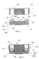
- FIG. 3 depicts a cross-sectional view of one embodiment of an OSA 132, similar to the OSAs depicted in FIGS. 1 and 2, which includes the passive alignment apparatus of the present invention.
- OSA 132 comprises three layers, an optical lens array 144 having a plurality of lenses 134, positioned between two spacers 146a-b.
- spacers 146a-b are configured from a material, such as silicon, Gallium Arsenide or any other material which is capable of being etched through any convenient etching technique, such as those known in the art.
- Spacers 146a-b are fixed or bound to lens array 144 through any convenient manner including adhesive, metal-to-metal bonding, glass seal, and any other manner known in the art.
- an opto-electronic device 150 Coupled to second spacer 146b, in one embodiment, is an opto-electronic device 150.
- the opto-electronic device may be various types of devices such as, but not limited to, Vertical Cavity Surface Emitting Lasers (VCSELs), other surface emitting devices, photo-detectors, and edge-emitting lasers.
- VCSELs Vertical Cavity Surface Emitting Lasers
- Opto-electronic device 150 may also be integrated devices combining one or more devices such as the combination of VCSELs and transistors, and photo-detectors and transistors.
- Opto-electronic device 150 is designed to transmit or receive optical signals to and from optical fibers 142 through lenses 134.
- Opto-electronic device 150 is positioned and secured to second spacer 146b, for example through soldering and other well known techniques, and will not be further described.
- first spacer 146a includes at least one etching or micromachining procedure.
- First spacer 146a is formed to include one or more positioning apertures 152.
- Positioning apertures 152 are etched through any convenient etching technique, including preferential etching, chemical etching and any other etching techniques known in the art. The formation of positioning apertures 152 through etching techniques allows positioning apertures 152 to be quickly and easily produced. Further, because etching is used, positioning apertures 152 are precisely located on interface surface 160 of first spacer 146a.
- first spacer 146a is formed through molding techniques as known in the art to include positioning apertures 152 at predefined locations within a high degree of precision.
- the alignment apparatus of the present invention implemented in OSA 132 further includes at least one alignment element 136.
- alignment element 136 is configured as alignment ball or bead 136.
- Alignment balls 136 are easily placed or positioned within positioning apertures 152 without the need for any further alignment, thus providing precise positioning of alignment balls 136 within interface surface 160 of OSA 132.
- Alignment balls 136 are fixed or secured within positioning apertures 152 through any convenient manner, including adhesive bonding, metal-to-metal bonding and any other manner known in the art.
- positioning apertures 152 are formed in precisely defined locations to within 3 and usually within 1 micron, thus allowing alignment balls 136 to be easily positioned within positioning apertures 152 while maintaining alignment balls 136 in a precise position.
- positioning apertures 152 are formed as a square V-shaped positioning apertures or pit as shown in FIGS. 4A and 4B.
- FIG. 4A shows a cross-sectional view of a portion of first spacer 146a including square V-shaped positioning aperture 152.
- FIG. 4B shows a top planar view of square V-shaped positioning aperture 136.
- Square V-shaped positioning apertures 152 are etched through known techniques which provide side walls 164 having a definite angle with respect to interface surface 160 regardless of the aperture size. Angled side walls 164 provide a plurality of advantages including precise positioning of alignment ball 136 within the center of positioning aperture 152, as well as compensating for slight manufacturing deviations from design parameters. Thus, if positioning aperture 152 or alignment ball 136 are slightly larger or smaller than ideal dimensions, an effective fit between alignment ball 136 and positioning aperture 152 is still maintained.
- Angled side walls 164 also allow a single size positioning aperture 152 to accommodate a plurality of different sized alignment balls 136 while still maintaining the precise accuracy needed. Angled side walls 164 further provide for simplified manufacturing and reduced construction time resulting in reduced costs as compared with the prior art alignment techniques because alignment balls 136 are easily positioned directly within the center of positioning aperture 152 and maintained within positioning apertures 152.
- FIG. 5 shows a top planar view of interface surface 160 of OSA 132, including two positioning apertures 152a and 152b each populated with an alignment ball 136a and 136b, respectively. Positioning apertures 152 can be formed in alternate shapes without departing from the inventive aspects of the present invention.
- positioning apertures 152 are formed as cylinders having vertical sides, or as circular V-shaped or cone shaped apertures which also provide precise placement of alignment balls and compensates for slight manufacturing deviations.
- positioning aperture is formed between ridges or other protruding structures which are etched to extend up from interface surface 160 such that alignment ball 136 is positioned between protruding ridges.
- positioning aperture 152 is formed such that positioning aperture 152 is a through-hole.
- each layer of the optical alignment component in one embodiment, is formed while in wafer form. Then the individual wafers comprising each layer of OSA 132 are combined to complete a plurality of optical alignment components which are easily separated into individual components.
- the assembly of OSA 132 is performed while spacers 146a-b and lens array 144 are in wafer form as is known in the art.
- spacer wafers and lens array wafers are formed including the etching of positioning apertures 152 in interface surface 160 of first spacer 146a, wafers are stacked and fixed or secured in position through any convenient bonding technique, including adhesive, metal-to-metal bond, glass seal and any other bonding technique known in the art.
- the alignment of spacer wafers with lens array wafer is achieved by aligning features of the wafers, as is known in the art.
- positioning apertures 152 are populated with alignment balls 136. Alignment balls 136 are fixed or secured into positioning apertures 152 though any convenient manner as described above. In one embodiment, alignment balls 136 are fixed into positioning apertures 152 prior to first spacer wafer being bound with lens array wafer.
- the stacked wafers include a plurality of individual, precisely configured and constructed OSAs 132. OSAs 132 are then separated through any convenient manner including wafer sawing.
- opto-electronic device 150 is fixed or soldered to second spacer 146b prior to the wafers being secured together. In an alternative embodiment, opto-electronic device 150 is fixed to second spacer 146b prior to separating the plurality of OSAs 132.
- OSAs 132 are self contained including I/O pads and optical alignment features.
- the single OSAs are individually testable and are capable, in this form, of being burned-in, thus allowing direct implementation into optical networks.
- OSAs are mass produced at substantially the same time through etching techniques which are substantially less expensive to manufacture than prior art techniques for aligning optical alignment components. Because the mass produced OSAs include the novel alignment apparatus, there is no need to actively align each OSA.
- the alignment apparatus and method of the present invention produces large numbers of optical alignment components with passive alignment capabilities providing greatly enhanced production and implementation at reduced costs. For example, a single, 6-inch composite wafer (including spacers 146a-b and lens array 144) provides for two thousand or more OSAs, similar to those shown in FIGS. 1 and 2 and described above. If each OSA includes 10 optics, the present apparatus and method provides for the substantially simultaneous alignment of 20,000 optics without the need to power the devices to obtain alignment. This is a vast improvement over the prior art which only allows for single optical alignment component alignment at one time where the component must be powered to be actively aligned.
- ferrule 130 is easily aligned utilizing the alignment balls 136 in cooperation with alignment or mating channels 140 to complete the alignment of optical fibers 142 with lenses 134.
- ferrule 130 is constructed to include alignment channels 140.
- Alignment balls 136 of OSA 132 are positioned to correspond with alignment channels 140 of ferrule 130.
- Ferrule 130 is formed through any convenient manner including molding and any other manner known in the art. In one embodiment, alignment balls 136 are positioned to correspond with previously existing molded ferrules 130, including those initially designed for use in the prior art pin-in-hole arrangement.
- Alignment channels 140 are formed in a cylindrical shape with a diameter which is substantially equal to the diameter of alignment ball 136 such that channel 140 fits around alignment ball 136, or rests on alignment ball 136 while alignment ball 136 partially extends into channel 140.
- channel diameter is slightly larger than the diameter of alignment ball allowing an x-axis ad y-axis positioning margin of shift while the margin of shift is within alignment tolerances to maintain alignment between fiber 142 and lens 134.
- alignment channel 140 is formed as a square tube having a width substantially equal to the diameter of alignment ball 136.
- alignment channel 140 can be formed in a variety of different configurations without departing from the inventive aspect of the present invention in providing cooperation with alignment ball 136, including, but not limited to, alignment channels formed as square V-shaped apertures similar to those formed in interface surface 160 of first spacer, or in a cone shape.
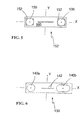
- alignment balls 136 provide accurate and precise alignment between a first optical alignment component, such as OSA 132, and a second optical alignment component, such as ferrule 130, where channels within ferrule are formed as a "hole-and-slot" configuration as shown in FIG. 6.
- a first channel 140a is a cylinder precisely molded to mate with an alignment ball 136.
- a second channel 140b is formed as a groove with a y-axis width precisely molded to mate with alignment ball 136 while the x-axis length allows the location of alignment ball 136 on first optical alignment component to vary.
- ferrule 130 described above and depicted in the figures are directed towards a multi-fiber ferrule.
- passive alignment of a single fiber ferrule can also be implemented through the same inventive method and apparatus described above without departing from the inventive aspects of the present invention.
- Alignment balls 136 are preferably configured as substantially spherical bodies to simplify construction of OSAs 132 as well as simplifying the mating of the OSAs 132 with ferrules 130.
- the spherical design allows for precise placement within the center of positioning aperture 152 without the need for any further manipulation to achieve the needed precision.
- Alignment balls 136 further ease alignment between the two optical alignment components by allowing channels to easily slip over sphere. Further, mating is eased because at initial cooperation between channel 140 and spherical alignment ball 136, channel 140 is larger than alignment ball 136 allowing channel 140 to easily slip over alignment ball 136.
- alignment balls 136 are configured as tapered, rectangular cubicles which are easily mated with ferrules 130.
- alignment ball 136 is formed as a pyramid, and a cubical diamond shape. It will be apparent to one skilled in the art that other configurations and shapes of alignment elements 136 can be implemented without departing from the inventive aspects of the present invention.
- Alignment balls can be formed in any size or diameter to provide accurate alignment with channels 140 and to maintain the alignment.
- Alignment balls 136 are constructed from substantially any convenient material which can be formed into a sphere having precise dimensions and sufficiently rigid to maintain alignment between the two components, including stainless steel, glass, sapphire, high carbon steel, ceramic, plastic and any other materials known in the art which allows precision formation and sufficient compression strength.
- a plurality of alignment balls are positioned on a single optical alignment component such that at least two of the alignment balls 136 have different diameters.
- an OSA 132 includes a first and second alignment ball where the first alignment ball has a larger diameter than the second alignment ball.
- OSA 132 includes an alignment ball 136 positioned within a positioning aperture 152 and an alignment channel 140
- ferrule 130 also includes an alignment ball 136 positioned within a positioning aperture 152 and an alignment channel 140, such that alignment ball 136 of OSA 132 is received by alignment channel 140 of ferrule 130 and alignment ball 136 of ferrule 130 is received by alignment channel 140 of OSA 132.
- positioning aperture 152 and alignment balls 136 are configured to replace the "pins" in the prior art "pin-in-hole” configuration.
Landscapes
- Physics & Mathematics (AREA)
- General Physics & Mathematics (AREA)
- Optics & Photonics (AREA)
- Optical Couplings Of Light Guides (AREA)
- Mounting And Adjusting Of Optical Elements (AREA)
Applications Claiming Priority (2)
| Application Number | Priority Date | Filing Date | Title |
|---|---|---|---|
| US687934 | 2000-10-13 | ||
| US09/687,934 US6526205B1 (en) | 2000-10-13 | 2000-10-13 | Method and apparatus for the passive alignment of optical components |
Publications (3)
| Publication Number | Publication Date |
|---|---|
| EP1197774A2 true EP1197774A2 (de) | 2002-04-17 |
| EP1197774A3 EP1197774A3 (de) | 2004-02-04 |
| EP1197774B1 EP1197774B1 (de) | 2006-12-13 |
Family
ID=24762447
Family Applications (1)
| Application Number | Title | Priority Date | Filing Date |
|---|---|---|---|
| EP01120406A Expired - Lifetime EP1197774B1 (de) | 2000-10-13 | 2001-08-27 | Verfahren und Anordnung für die passive Ausrichtung optischer Komponenten |
Country Status (5)
| Country | Link |
|---|---|
| US (1) | US6526205B1 (de) |
| EP (1) | EP1197774B1 (de) |
| JP (1) | JP2002182088A (de) |
| KR (1) | KR20020029627A (de) |
| DE (1) | DE60125123T2 (de) |
Families Citing this family (15)
| Publication number | Priority date | Publication date | Assignee | Title |
|---|---|---|---|---|
| US6740495B1 (en) * | 2000-04-03 | 2004-05-25 | Rigel Pharmaceuticals, Inc. | Ubiquitin ligase assay |
| JP2002202440A (ja) * | 2000-12-28 | 2002-07-19 | Japan Aviation Electronics Industry Ltd | 光モジュールの実装構造及び実装方法 |
| US7040814B2 (en) * | 2001-10-15 | 2006-05-09 | The Furukawa Electric Co., Ltd. | Functional optical module |
| US6764227B2 (en) * | 2002-03-07 | 2004-07-20 | Agilent Technologies, Inc. | Interconnecting optical components with passive alignment |
| JP4364594B2 (ja) * | 2003-03-18 | 2009-11-18 | セイコーインスツル株式会社 | 光デバイスおよびその製造方法 |
| JP4697698B2 (ja) * | 2003-11-07 | 2011-06-08 | セイコーインスツル株式会社 | 光デバイスおよびその製造方法 |
| US7454105B2 (en) * | 2004-11-22 | 2008-11-18 | Avago Technologies Fiber Ip (Singapore) Pte. Ltd. | Passive alignment using elastic averaging in optoelectronics applications |
| JP4744211B2 (ja) * | 2005-07-08 | 2011-08-10 | 独立行政法人産業技術総合研究所 | 光モジュール |
| US7619312B2 (en) * | 2005-10-03 | 2009-11-17 | Sun Microsystems, Inc. | Method and apparatus for precisely aligning integrated circuit chips |
| US9250399B2 (en) * | 2006-08-31 | 2016-02-02 | Optogig, Inc. | High density active modular optoelectronic device for use with push-release mechanism and method for using same |
| CN102089690A (zh) | 2008-05-09 | 2011-06-08 | 惠普开发有限公司 | 接近自由空间光学互连 |
| US8669633B2 (en) * | 2010-07-28 | 2014-03-11 | Teledyne Dalsa, Inc. | Packaged device with an image sensor aligned to a faceplate using fiducial marks and connection bodies registered thereto |
| US9620934B2 (en) | 2010-08-31 | 2017-04-11 | Avago Technologies General Ip (Singapore) Pte. Ltd. | Flip-chip assembly comprising an array of vertical cavity surface emitting lasers (VCSELs) |
| US9188751B2 (en) * | 2010-08-31 | 2015-11-17 | Avago Technologies General Ip (Singapore) Pte. Ltd. | Flip-chip assembly comprising an array of vertical cavity surface emitting lasers (VCSELSs), and an optical transmitter assembly that incorporates the flip-chip assembly |
| WO2016018363A1 (en) | 2014-07-31 | 2016-02-04 | Hewlett-Packard Development Company, L. P. | Interposer registration elements |
Family Cites Families (8)
| Publication number | Priority date | Publication date | Assignee | Title |
|---|---|---|---|---|
| AU635172B2 (en) * | 1991-05-13 | 1993-03-11 | Nippon Telegraph & Telephone Corporation | Multifiber optical connector plug with low reflection and low insertion loss |
| US5179609A (en) * | 1991-08-30 | 1993-01-12 | At&T Bell Laboratories | Optical assembly including fiber attachment |
| US5259054A (en) * | 1992-01-10 | 1993-11-02 | At&T Bell Laboratories | Self-aligned optical subassembly |
| US5778123A (en) * | 1996-03-12 | 1998-07-07 | Minnesota Mining And Manufacturing Company | Alignment assembly for multifiber or single fiber optical cable connector |
| JP3824797B2 (ja) * | 1999-01-08 | 2006-09-20 | 古河電気工業株式会社 | 受発光素子モジュール |
| US6454469B1 (en) * | 1999-06-29 | 2002-09-24 | International Business Machines Corporation | Actively aligned optical coupling assembly |
| US6234687B1 (en) * | 1999-08-27 | 2001-05-22 | International Business Machines Corporation | Self-aligning method and interlocking assembly for attaching an optoelectronic device to a coupler |
| US6450704B1 (en) * | 2000-10-05 | 2002-09-17 | Corona Optical Systems, Inc. | Transparent substrate and hinged optical assembly |
-
2000
- 2000-10-13 US US09/687,934 patent/US6526205B1/en not_active Expired - Lifetime
-
2001
- 2001-08-27 DE DE60125123T patent/DE60125123T2/de not_active Expired - Lifetime
- 2001-08-27 EP EP01120406A patent/EP1197774B1/de not_active Expired - Lifetime
- 2001-10-12 KR KR1020010062950A patent/KR20020029627A/ko not_active Ceased
- 2001-10-15 JP JP2001316692A patent/JP2002182088A/ja not_active Withdrawn
Also Published As
| Publication number | Publication date |
|---|---|
| JP2002182088A (ja) | 2002-06-26 |
| US6526205B1 (en) | 2003-02-25 |
| DE60125123D1 (de) | 2007-01-25 |
| DE60125123T2 (de) | 2007-10-25 |
| KR20020029627A (ko) | 2002-04-19 |
| EP1197774A3 (de) | 2004-02-04 |
| EP1197774B1 (de) | 2006-12-13 |
Similar Documents
| Publication | Publication Date | Title |
|---|---|---|
| US6526205B1 (en) | Method and apparatus for the passive alignment of optical components | |
| US10429597B2 (en) | Interposer assemblies and arrangements for coupling at least one optical fiber to at least one optoelectronic device | |
| US6328482B1 (en) | Multilayer optical fiber coupler | |
| US8360659B2 (en) | Fiber-optic pin-and-socket connector having a beam expansion device | |
| US6234687B1 (en) | Self-aligning method and interlocking assembly for attaching an optoelectronic device to a coupler | |
| US5907650A (en) | High precision optical fiber array connector and method | |
| US9563028B2 (en) | Method to manufacture an optoelectronic assembly | |
| JP3824797B2 (ja) | 受発光素子モジュール | |
| US6456761B2 (en) | Apparatus, assembly, and method for making micro-fixtured lensed assembly for optoelectronic devices and optical fibers | |
| CA2380240C (en) | Method and device for passive alignment | |
| WO2014176472A1 (en) | Optical fiber subassembly | |
| JP2001215358A (ja) | 光ファイバ用フェルール及びその製造方法 | |
| US5522001A (en) | Optical fiber coupled devices and method of assembling same | |
| US20060097137A1 (en) | True position bench | |
| US10291332B2 (en) | Self-aligned silicon fiber optic connector | |
| WO2003005085A1 (en) | Integration of fused collimated coupler for use in opto-electronic modules | |
| US20040213523A1 (en) | Multi-piece fiber optic component and manufacturing technique | |
| US6764227B2 (en) | Interconnecting optical components with passive alignment | |
| Han et al. | Integration of silicon bench micro-optics | |
| EP2762937A1 (de) | Verfahren zum Herstellen einer optoelektronischen Anordnung | |
| US20250306294A1 (en) | On-Package Self-Aligning Expanded-Beam Connector | |
| Sasaki et al. | Marker alignment method for passive laser coupling on silicon waferboard | |
| KR100456468B1 (ko) | 레이저 미세가공을 이용한 광송수신 모듈 및 그 제조 방법 | |
| Morimoto et al. | Design And Fabrication Of Low Loss Single-Mode Optical Fiber Connector | |
| CN113281854A (zh) | 具有透镜阵列的套圈组件 |
Legal Events
| Date | Code | Title | Description |
|---|---|---|---|
| PUAI | Public reference made under article 153(3) epc to a published international application that has entered the european phase |
Free format text: ORIGINAL CODE: 0009012 |
|
| AK | Designated contracting states |
Kind code of ref document: A2 Designated state(s): AT BE CH CY DE DK ES FI FR GB GR IE IT LI LU MC NL PT SE TR |
|
| AX | Request for extension of the european patent |
Free format text: AL;LT;LV;MK;RO;SI |
|
| RAP1 | Party data changed (applicant data changed or rights of an application transferred) |
Owner name: AGILENT TECHNOLOGIES, INC. (A DELAWARE CORPORATION |
|
| PUAL | Search report despatched |
Free format text: ORIGINAL CODE: 0009013 |
|
| AK | Designated contracting states |
Kind code of ref document: A3 Designated state(s): AT BE CH CY DE DK ES FI FR GB GR IE IT LI LU MC NL PT SE TR |
|
| AX | Request for extension of the european patent |
Extension state: AL LT LV MK RO SI |
|
| 17P | Request for examination filed |
Effective date: 20040511 |
|
| 17Q | First examination report despatched |
Effective date: 20040716 |
|
| AKX | Designation fees paid |
Designated state(s): DE FR GB |
|
| GRAP | Despatch of communication of intention to grant a patent |
Free format text: ORIGINAL CODE: EPIDOSNIGR1 |
|
| GRAS | Grant fee paid |
Free format text: ORIGINAL CODE: EPIDOSNIGR3 |
|
| GRAA | (expected) grant |
Free format text: ORIGINAL CODE: 0009210 |
|
| AK | Designated contracting states |
Kind code of ref document: B1 Designated state(s): DE FR GB |
|
| REG | Reference to a national code |
Ref country code: GB Ref legal event code: FG4D |
|
| RAP2 | Party data changed (patent owner data changed or rights of a patent transferred) |
Owner name: AVAGO TECHNOLOGIES FIBER IP (SINGAPORE) PTE. LTD. |
|
| REF | Corresponds to: |
Ref document number: 60125123 Country of ref document: DE Date of ref document: 20070125 Kind code of ref document: P |
|
| REG | Reference to a national code |
Ref country code: GB Ref legal event code: ERR Free format text: NOTIFICATION HAS NOW BEEN RECEIVED FROM THE EUROPEAN PATENT OFFICE THAT THE CORRECT NAME IS: AVAGO TECHNOLOGIES FIBER IP (SINGAPORE) PTE, LTD THIS CORRECTION WAS PUBLISHED IN THE EUROPEAN PATENT BULLETIN 06/52 DATED 20061227 |
|
| ET | Fr: translation filed | ||
| PLBE | No opposition filed within time limit |
Free format text: ORIGINAL CODE: 0009261 |
|
| STAA | Information on the status of an ep patent application or granted ep patent |
Free format text: STATUS: NO OPPOSITION FILED WITHIN TIME LIMIT |
|
| 26N | No opposition filed |
Effective date: 20070914 |
|
| REG | Reference to a national code |
Ref country code: FR Ref legal event code: ST Effective date: 20080430 |
|
| PG25 | Lapsed in a contracting state [announced via postgrant information from national office to epo] |
Ref country code: FR Free format text: LAPSE BECAUSE OF NON-PAYMENT OF DUE FEES Effective date: 20070831 |
|
| REG | Reference to a national code |
Ref country code: DE Ref legal event code: R082 Ref document number: 60125123 Country of ref document: DE Representative=s name: DILG HAEUSLER SCHINDELMANN PATENTANWALTSGESELL, DE |
|
| REG | Reference to a national code |
Ref country code: DE Ref legal event code: R082 Ref document number: 60125123 Country of ref document: DE Representative=s name: DILG HAEUSLER SCHINDELMANN PATENTANWALTSGESELL, DE Effective date: 20130702 Ref country code: DE Ref legal event code: R081 Ref document number: 60125123 Country of ref document: DE Owner name: AVAGO TECHNOLOGIES GENERAL IP (SINGAPORE) PTE., SG Free format text: FORMER OWNER: AVAGO TECHNOLOGIES FIBER IP (SINGAPORE) PTE. LTD., SINGAPORE, SG Effective date: 20130702 |
|
| PGFP | Annual fee paid to national office [announced via postgrant information from national office to epo] |
Ref country code: GB Payment date: 20150724 Year of fee payment: 15 |
|
| GBPC | Gb: european patent ceased through non-payment of renewal fee |
Effective date: 20160827 |
|
| PG25 | Lapsed in a contracting state [announced via postgrant information from national office to epo] |
Ref country code: GB Free format text: LAPSE BECAUSE OF NON-PAYMENT OF DUE FEES Effective date: 20160827 |
|
| REG | Reference to a national code |
Ref country code: DE Ref legal event code: R082 Ref document number: 60125123 Country of ref document: DE Representative=s name: DILG, HAEUSLER, SCHINDELMANN PATENTANWALTSGESE, DE Ref country code: DE Ref legal event code: R081 Ref document number: 60125123 Country of ref document: DE Owner name: BROADCOM INTERNATIONAL PTE. LTD., SG Free format text: FORMER OWNER: AVAGO TECHNOLOGIES GENERAL IP (SINGAPORE) PTE. LTD., SINGAPORE, SG Ref country code: DE Ref legal event code: R082 Ref document number: 60125123 Country of ref document: DE Representative=s name: DILG HAEUSLER SCHINDELMANN PATENTANWALTSGESELL, DE Ref country code: DE Ref legal event code: R081 Ref document number: 60125123 Country of ref document: DE Owner name: AVAGO TECHNOLOGIES INTERNATIONAL SALES PTE. LT, SG Free format text: FORMER OWNER: AVAGO TECHNOLOGIES GENERAL IP (SINGAPORE) PTE. LTD., SINGAPORE, SG |
|
| REG | Reference to a national code |
Ref country code: DE Ref legal event code: R082 Ref document number: 60125123 Country of ref document: DE Representative=s name: DILG, HAEUSLER, SCHINDELMANN PATENTANWALTSGESE, DE Ref country code: DE Ref legal event code: R081 Ref document number: 60125123 Country of ref document: DE Owner name: BROADCOM INTERNATIONAL PTE. LTD., SG Free format text: FORMER OWNER: AVAGO TECHNOLOGIES INTERNATIONAL SALES PTE. LTD., SINGAPUR, SG |
|
| PGFP | Annual fee paid to national office [announced via postgrant information from national office to epo] |
Ref country code: DE Payment date: 20200827 Year of fee payment: 20 |
|
| REG | Reference to a national code |
Ref country code: DE Ref legal event code: R071 Ref document number: 60125123 Country of ref document: DE |