EP1197296A2 - Pad conditioning disk - Google Patents
Pad conditioning disk Download PDFInfo
- Publication number
- EP1197296A2 EP1197296A2 EP01307888A EP01307888A EP1197296A2 EP 1197296 A2 EP1197296 A2 EP 1197296A2 EP 01307888 A EP01307888 A EP 01307888A EP 01307888 A EP01307888 A EP 01307888A EP 1197296 A2 EP1197296 A2 EP 1197296A2
- Authority
- EP
- European Patent Office
- Prior art keywords
- end effector
- crystals
- backing plate
- polishing pad
- matrix material
- Prior art date
- Legal status (The legal status is an assumption and is not a legal conclusion. Google has not performed a legal analysis and makes no representation as to the accuracy of the status listed.)
- Withdrawn
Links
Images


Classifications
-
- B—PERFORMING OPERATIONS; TRANSPORTING
- B24—GRINDING; POLISHING
- B24B—MACHINES, DEVICES, OR PROCESSES FOR GRINDING OR POLISHING; DRESSING OR CONDITIONING OF ABRADING SURFACES; FEEDING OF GRINDING, POLISHING, OR LAPPING AGENTS
- B24B53/00—Devices or means for dressing or conditioning abrasive surfaces
- B24B53/017—Devices or means for dressing, cleaning or otherwise conditioning lapping tools
-
- H—ELECTRICITY
- H10—SEMICONDUCTOR DEVICES; ELECTRIC SOLID-STATE DEVICES NOT OTHERWISE PROVIDED FOR
- H10P—GENERIC PROCESSES OR APPARATUS FOR THE MANUFACTURE OR TREATMENT OF DEVICES COVERED BY CLASS H10
- H10P52/00—Grinding, lapping or polishing of wafers, substrates or parts of devices
-
- B—PERFORMING OPERATIONS; TRANSPORTING
- B24—GRINDING; POLISHING
- B24D—TOOLS FOR GRINDING, BUFFING OR SHARPENING
- B24D18/00—Manufacture of grinding tools or other grinding devices, e.g. wheels, not otherwise provided for
Definitions
- the present invention relates to the field of polishing pad conditioners, and more particularly to an improved end effector for conditioning pads used to polish the surface of semiconductor wafers or semiconductor devices, glass substrates and the like.
- a semiconductor wafer is planarized or "polished" using a chemical mechanical polishing apparatus that presses a surface of the wafer against a surface of an abrasive pad and that moves the surface of the wafer relative to the surface of the abrasive pad.
- the surface of the abrasive pad may become compacted and lose its abrasive quality.
- Such compaction reduces the quality and efficiency of the polishing process.
- the abrasive pad is conditioned or roughened (in situ or ex situ) via a device known as a pad conditioning end effector.
- the end effector comprises one or more diamond crystals held by mechanical means (e.g., by screw type holding mechanisms).
- the diamond crystals are pressed against the surface of the polishing pad and are moved relative to the surface of the polishing pad.
- the crystals are necessarily relatively large and provide less than optimal pad conditioning. Accordingly, an improved pad conditioning end effector is needed.
- an inventive end effector for conditioning a polishing pad.
- the end effector comprises a backing plate, a matrix material adhered to a first surface of the backing plate, and a plurality of crystals embedded in the matrix material an amount sufficient to prevent the plurality of crystals from becoming dislodged from the matrix material during pad conditioning.
- the plurality of crystals have an absolute crystal height distribution that may be skewed toward zero.
- FIG. 1A is a side view of a conventional end effector in contact with an abrasive pad.
- FIG. 1B illustrates a close-up view of the conventional end effector of FIG. 1A.
- FIG. 1C illustrates an exemplary distribution of absolute crystal heights for the conventional end effector of FIGS. 1A and 1B.
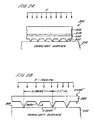
- FIG. 2A illustrates a side view of a first embodiment of an inventive end effector shown in contact with a compliant surface.
- FIG. 2B illustrates a side view of a second embodiment of an inventive end effector shown in contact with a compliant surface.
- FIG. 3 shows a top plan view of a semiconductor device polishing apparatus which employs the inventive end effector of FIGS. 2A and 2B.
- FIG. 1A is a side view of a conventional end effector 100 in contact with an abrasive pad 102.
- the conventional end effector 100 includes a plurality of diamond crystals 104 that extend from a backing plate 106 of the end effector 100 toward the abrasive pad 102.
- FIG. 1B illustrates a close-up view of the conventional end effector 100 of FIG. 1A.
- each of the diamond crystals 104 of the conventional end effector 100 may extend from the backing plate 106 by a different amount, and some of the crystals do not contact the abrasive pad 102. Accordingly, these "non-contacting" crystals cannot roughen the surface of the abrasive pad 102 during pad conditioning.
- the height (H) of a diamond crystal above the abrasive pad 102 when the end effector 100 is placed in contact with the abrasive pad 102 is termed the "absolute crystal height" of the crystal.
- a crystal that contacts the abrasive pad 102 such as crystal 104a in FIG. 1B
- FIG. 1C illustrates an exemplary distribution 108 of absolute crystal heights (absolute crystal height distribution 108) for the conventional end effector 100 of FIGS. 1A and 1B.
- the "mean" absolute crystal height is shown as M in FIG. 1C.
- the mean absolute crystal height of an end effector is zero (e.g., all crystals of the end effector contact the abrasive pad 102).
- any technique that can "skew" the absolute crystal height distribution of an end effector toward zero e.g., as shown by the exemplary absolute crystal height distribution 110 of FIG. 1C which has a mean absolute crystal height of M'
- the resulting end effector may uniformly and efficiently condition a polishing pad (e.g., as more crystals will contact the abrasive pad during pad conditioning).
- an inventive end effector 200 has a plurality of crystals 202 (e.g., diamonds) embedded in a matrix material (e.g., a metal substrate 204 such as a nickel alloy matrix material as is known in the art) an amount sufficient to prevent the plurality of crystals from becoming dislodged from the matrix material during pad conditioning.
- a matrix material e.g., a metal substrate 204 such as a nickel alloy matrix material as is known in the art
- the matrix material may comprise any suitable matrix material, the crystals may be, for example, 9 mil. in height and the crystals may extend, for example, about 2.5 to 3.5 mils from the matrix material with a standard deviation of about 0.75 mil. The height each crystal extends from the matrix material is termed the exposure height of the crystal.
- the end effector 200 also has an absolute crystal height distribution skewed toward zero.
- an absolute crystal height distribution of the end effector 200 may be skewed toward zero by: (1) obtaining the metal alloy substrate 204 having the crystals 202 extending therefrom with a first absolute crystal height distribution (e.g., the absolute crystal height distribution 108 of FIG.
- the metal alloy substrate 204 will deflect slightly at locations wherein a crystal does not touch the compliant surface 210 (e.g., at locations of the polishing pad having a large absolute crystal height), the absolute crystal height distribution of the end effector 200 will be skewed toward zero as shown by the absolute crystal height distribution 110 of FIG. 1C (relative to a normal "bell curve" distribution 108) as crystals that do not contact the surface 210 will move toward the surface 210 (e.g., crystal 202a in FIG. 2B).
- the metal alloy substrate 204 comprises a nickel alloy having a thickness of about 0.032 inches with diamond crystals 202 spaced by about 0.1 inches as shown in FIG. 2B.
- the mean absolute crystal height distribution of the diamond crystals 202 before curing may be about 1.5 mils, the average diamond crystal size may be about 9 mils and the average exposure height of each diamond crystal may be about 3 to 3.5 mils with a standard deviation of about 0.75 mil or less.
- the metal backing plate 206 may be a stainless steel backing plate having a thickness of about 0.2 inches and the bonding material 208 comprises a conventional bonding material (as is known in the art) having a thickness of about 0.5 to 2 mils.
- the bonding material 208 may be cured, for example, by heating the bonding material 208 (e.g., to a curing temperature set by the manufacturer of the bonding material 208) while a force of about 1000 pounds per square inch may be applied to the backing plate 206. Following curing under the application of the 1000 pounds per square inch force, the mean absolute crystal height distribution of the diamond crystals 202 may be about 0.75 mils. Deviations resulting from deflection of the metal substrate 204 will be filled by the bonding material 208.
- a substrate may be coated with an adhesive and then may be contacted with the abrasive particles (e.g., diamond crystals).
- the adhered crystals may be oriented, for example, by shaking/vibrating the substrate such that the adhered crystals assume a stable position, and/or by applying a magnetic force such that the crystals may be aligned according to their crystallographic structure and according to lines of magnetic force.
- the crystals may be sprayed with an adhesive, or sprayed with a liquid which may be subsequently frozen, so as to maintain the crystals' orientation. Thereafter, to permanently hold the crystals, the crystals may be contacted with a sinterable or fusible material (possibly in the form of a preform) and heat and/or pressure may be applied to complete the abrasive material.
- a sinterable or fusible material possibly in the form of a preform
- FIG. 3 shows a top plan view of a semiconductor device polishing apparatus 300 which employs the inventive end effector 200 of FIGS. 2A and 2B.
- the polishing apparatus 300 comprises a polishing pad 302 which rotates about a center point 304 at a given speed.
- the polishing pad 302 has a plurality of grooves 306 formed in the top surface of the polishing pad 302. These grooves aid the channeling of an abrasive slurry across the surface of the pad.
- the abrasive slurry (not shown) is supplied via an inlet 308.
- a conditioning arm 310 may be rotatably disposed along the side of the polishing pad 302.
- the inventive end effector 200 may be mounted to the conditioning arm 310 (e.g., via screws attached to the backing plate 206).
- the polishing pad 302 may be conditioned during the polishing of the semiconductor device (i.e., in situ conditioning) or during a separate pad conditioning step (i.e., ex situ conditioning).
- in situ conditioning a wafer 312 may be mounted along one side of the end effector 200 and rotates in a first direction while being swept radially across the surface of the polishing pad 302.
- the polishing pad 302 rotates as the slurry (not shown) is supplied to the surface of the polishing pad via the inlet 308.
- the conditioning arm 310 sweeps the inventive end effector 200, which in one embodiment may rotate in the same direction the pad rotates, radially across the surface of the polishing pad 302 while applying a downward force.
- the end effector 200 rotates at a rate of 20-120 r.p.m. and may be pressed against the polishing pad 302 with a downward force of 5-10 pounds given the area of the end effector and density of crystals.
- the inventive end effector 200 with its skewed absolute crystal height distribution, may provide a desired balance of polishing pad surface roughening, so that a consistent polish rate may be maintained, and of polishing pad life, so that material and downtime costs may be minimized.
- crystals which extend farthest from the metal substrate 204 will wear as the crystals contact the polishing pad first.
- the skew of the absolute crystal height distribution may ensure that the polishing pad 302 may be continuously contacted by "sharp" crystal surfaces.
- a mechanism for moving the end effector across the polishing pad is to be construed broadly to cover movement of the end effector and/or movement (e.g., rotary, linear, etc.) of the polishing pad.
- the invention applies to any end effector having a plurality of crystals as described herein. Any known technique may be employed to adhere the substrate 204 to the backing plate 206 (e.g., such as via use of any conventional compliant bonding material), and other crystal exposure heights may be employed. In at least one embodiment of the invention, an average crystal exposure height of 1 mil. or greater may be employed. Other crystal spacings may be employed, and the force applied to the backing plate 206 may be varied (e.g., depending on the crystal spacing, the backing plate thickness, etc.).
- the matrix material 204 alternatively may be a polymer.
- the polymer When used in connection with the polishing of oxide layers the polymer may be chemically inert so that it is not reactive with the polishing slurry. Further, should polymer particles become embedded on the surface of a silicon wafer being polished, the polymer particles (unlike particles of a metal matrix) will not act as a conductor. For an oxide polish the polymer's modulus may be substantially less than the modulus of oxide, fused silicon, or quartz. Further, the matrix 15 may be treated to resist corrosion.
- the term matrix, as used herein refers to any material in which diamonds may be embedded. The crystals may be approximately the same size or may vary in size.
- a known amount of crystals may be applied to the matrix, may be embedded a predetermined amount (e.g., 75 percent of the crystal's height) so as to substantially deter or prevent crystal dislodgment during normal polishing conditions, and may be approximately evenly spaced, as taught by U.S. Patent Application Serial No. 09/241,910 titled “Improved End Effector for Pad Conditioning", filed on February 2, 1999, the entire disclosure of which is incorporated herein by reference.
- the average absolute crystal height distribution may be selected so as to introduce new cutting edges at a rate that produces approximately constant pad wear during pad conditioning and/or during polishing (e.g., a skewed absolute crystal height distribution may introduce new (and more) cutting edges faster than a "normal" absolute crystal height distribution as cutting edges round during pad conditioning and/or during chemical mechanical polishing).
- the average absolute crystal height distribution may be selected so that the number of cutting edges that contact a pad during conditioning remains approximately constant for an approximately constant force applied to the end effector 200 (e.g., despite rounding of the crystals 202 during conditioning).
Landscapes
- Engineering & Computer Science (AREA)
- Mechanical Engineering (AREA)
- Manufacturing & Machinery (AREA)
- Finish Polishing, Edge Sharpening, And Grinding By Specific Grinding Devices (AREA)
- Mechanical Treatment Of Semiconductor (AREA)
- Grinding-Machine Dressing And Accessory Apparatuses (AREA)
- Polishing Bodies And Polishing Tools (AREA)
Abstract
Description
Claims (18)
- An end effector (200) for conditioning a polishing pad (102), comprising:a backing plate (206);a matrix material adhered to a first surface of the backing plate (206); anda plurality of crystals (202) embedded in the matrix material; wherein the plurality of crystals (202) have an absolute crystal height distribution (108) that is skewed toward zero.
- The end effector of claim 1 wherein the backing plate (206) comprises stainless steel.
- The end effector of claim 2 wherein the backing plate (206) has a thickness of about 0.2 inches (5 mm).
- The end effector of claim 1, claim 2 or claim 3, wherein the matrix material comprises a metal substrate (204).
- The end effector of claim 4 wherein the metal substrate (204) comprises a nickel alloy.
- The end effector of claim 5 wherein the metal substrate (204) has a thickness of about 0.032 inches (813 µm).
- The end effector of any preceding claim, wherein the plurality of crystals (202) are spaced by about 0.1 inches (2.5 mm).
- The end effector of any preceding claim, wherein the plurality of crystals (202) have an average exposure height of about 3 to 3.5 mils (76 to 89 µm) with a standard deviation of about 0.75 mil (19 µm) or less.
- The end effector of any preceding claim, wherein the matrix material is adhered to the backing plate (206) with a bonding material (208).
- The end effector of claim 9 wherein the bonding material (208) comprises a heat-curable bonding material.
- The end effector of claim 10 wherein the bonding material (208) has a thickness of about 0.5 to 2 mils (13 to 51 µm).
- The end effector of any preceding claim, wherein the plurality of crystals (202) have a mean absolute crystal height distribution of about 0.75 mils (19 µm).
- An apparatus comprising:an inlet (308) adapted to supply a slurry to a polishing pad (302);a conditioning arm (310) disposed along the polishing pad (310); andthe end effector (200) of any one of the preceding claims, coupled to the conditioning arm (310) and adapted to condition the polishing pad (302).
- A method of forming an end effector comprising:obtaining a matrix material having a plurality of crystals (202) extending from a first side of the matrix material, the plurality of crystals (202) having a first absolute crystal height distribution (108);bonding a second side of the matrix material to a backing plate (206) using a bonding material (208) ;contacting at least a portion of the plurality of crystals (202) to a surface (210);applying a force to the backing plate (206) so as to press the at least a portion of the plurality of crystals (202) against the surface; andallowing the bonding material (208) to cure during the step of applying the force.
- The method of claim 14 wherein the surface (210) comprises polyurethane.
- The method of claim 14 wherein the force exerts a pressure of about 1000 pounds per square inch (6.9 MPa).
- An end effector (200) formed from the method of any one of claims 14 to 16.
- A method of conditioning a polishing pad (302) comprising:providing a polishing pad (302); andcontacting the polishing pad (302) with a conditioner comprising a plurality of crystals (202) embedded in a matrix material such that the plurality of crystals (202) have an absolute crystal height distribution (108) that is skewed toward zero.
Applications Claiming Priority (2)
| Application Number | Priority Date | Filing Date | Title |
|---|---|---|---|
| US09/684,141 US6551176B1 (en) | 2000-10-05 | 2000-10-05 | Pad conditioning disk |
| US684141 | 2003-10-10 |
Publications (2)
| Publication Number | Publication Date |
|---|---|
| EP1197296A2 true EP1197296A2 (en) | 2002-04-17 |
| EP1197296A3 EP1197296A3 (en) | 2003-12-17 |
Family
ID=24746846
Family Applications (1)
| Application Number | Title | Priority Date | Filing Date |
|---|---|---|---|
| EP01307888A Withdrawn EP1197296A3 (en) | 2000-10-05 | 2001-09-17 | Pad conditioning disk |
Country Status (5)
| Country | Link |
|---|---|
| US (1) | US6551176B1 (en) |
| EP (1) | EP1197296A3 (en) |
| JP (1) | JP2002178259A (en) |
| KR (1) | KR20020027268A (en) |
| TW (1) | TW546183B (en) |
Families Citing this family (34)
| Publication number | Priority date | Publication date | Assignee | Title |
|---|---|---|---|---|
| US9199357B2 (en) | 1997-04-04 | 2015-12-01 | Chien-Min Sung | Brazed diamond tools and methods for making the same |
| US9463552B2 (en) | 1997-04-04 | 2016-10-11 | Chien-Min Sung | Superbrasvie tools containing uniformly leveled superabrasive particles and associated methods |
| US9221154B2 (en) | 1997-04-04 | 2015-12-29 | Chien-Min Sung | Diamond tools and methods for making the same |
| US9409280B2 (en) | 1997-04-04 | 2016-08-09 | Chien-Min Sung | Brazed diamond tools and methods for making the same |
| US9868100B2 (en) | 1997-04-04 | 2018-01-16 | Chien-Min Sung | Brazed diamond tools and methods for making the same |
| US9238207B2 (en) | 1997-04-04 | 2016-01-19 | Chien-Min Sung | Brazed diamond tools and methods for making the same |
| US7201645B2 (en) * | 1999-11-22 | 2007-04-10 | Chien-Min Sung | Contoured CMP pad dresser and associated methods |
| US6847041B2 (en) * | 2001-02-09 | 2005-01-25 | Canon Kabushiki Kaisha | Scintillator panel, radiation detector and manufacture methods thereof |
| JP2002299289A (en) * | 2001-03-30 | 2002-10-11 | Toshiba Corp | Chemical mechanical polishing method and semiconductor device manufacturing method |
| US6764389B1 (en) * | 2002-08-20 | 2004-07-20 | Lsi Logic Corporation | Conditioning bar assembly having an abrasion member supported on a polycarbonate member |
| US20040045419A1 (en) * | 2002-09-10 | 2004-03-11 | Bryan William J. | Multi-diamond cutting tool assembly for creating microreplication tools |
| US6945857B1 (en) | 2004-07-08 | 2005-09-20 | Applied Materials, Inc. | Polishing pad conditioner and methods of manufacture and recycling |
| US7097542B2 (en) | 2004-07-26 | 2006-08-29 | Intel Corporation | Method and apparatus for conditioning a polishing pad |
| US7089925B1 (en) | 2004-08-18 | 2006-08-15 | Kinik Company | Reciprocating wire saw for cutting hard materials |
| US7066795B2 (en) * | 2004-10-12 | 2006-06-27 | Applied Materials, Inc. | Polishing pad conditioner with shaped abrasive patterns and channels |
| US8393934B2 (en) * | 2006-11-16 | 2013-03-12 | Chien-Min Sung | CMP pad dressers with hybridized abrasive surface and related methods |
| US8678878B2 (en) | 2009-09-29 | 2014-03-25 | Chien-Min Sung | System for evaluating and/or improving performance of a CMP pad dresser |
| US9138862B2 (en) | 2011-05-23 | 2015-09-22 | Chien-Min Sung | CMP pad dresser having leveled tips and associated methods |
| US8974270B2 (en) | 2011-05-23 | 2015-03-10 | Chien-Min Sung | CMP pad dresser having leveled tips and associated methods |
| US8398466B2 (en) | 2006-11-16 | 2013-03-19 | Chien-Min Sung | CMP pad conditioners with mosaic abrasive segments and associated methods |
| US9724802B2 (en) | 2005-05-16 | 2017-08-08 | Chien-Min Sung | CMP pad dressers having leveled tips and associated methods |
| US8622787B2 (en) * | 2006-11-16 | 2014-01-07 | Chien-Min Sung | CMP pad dressers with hybridized abrasive surface and related methods |
| US20140120807A1 (en) * | 2005-05-16 | 2014-05-01 | Chien-Min Sung | Cmp pad conditioners with mosaic abrasive segments and associated methods |
| TWI290337B (en) * | 2005-08-09 | 2007-11-21 | Princo Corp | Pad conditioner for conditioning a CMP pad and method of making the same |
| US20080014845A1 (en) * | 2006-07-11 | 2008-01-17 | Alpay Yilmaz | Conditioning disk having uniform structures |
| US7410411B2 (en) * | 2006-09-28 | 2008-08-12 | Araca, Incorporated | Method of determining the number of active diamonds on a conditioning disk |
| US7815495B2 (en) * | 2007-04-11 | 2010-10-19 | Applied Materials, Inc. | Pad conditioner |
| TWI388402B (en) | 2007-12-06 | 2013-03-11 | Methods for orienting superabrasive particles on a surface and associated tools | |
| US8550879B2 (en) * | 2008-10-23 | 2013-10-08 | Applied Materials, Inc. | Polishing pad conditioner |
| WO2012040373A2 (en) | 2010-09-21 | 2012-03-29 | Ritedia Corporation | Diamond particle mololayer heat spreaders and associated methods |
| WO2016164498A1 (en) * | 2015-04-06 | 2016-10-13 | M Cubed Technologies, Inc. | Article having diamond-only contact surfaces |
| US12054439B2 (en) | 2020-04-28 | 2024-08-06 | Ii-Vi Delaware, Inc. | Ceramic substrate with reaction-bonded silicon carbide having diamond particles |
| US11584694B2 (en) | 2021-01-19 | 2023-02-21 | Ii-Vi Delaware, Inc. | Silicon carbide body with localized diamond reinforcement |
| US12338187B2 (en) | 2023-01-17 | 2025-06-24 | Ii-Vi Delaware, Inc. | Multi-component device and method of making a multi-component device |
Family Cites Families (27)
| Publication number | Priority date | Publication date | Assignee | Title |
|---|---|---|---|---|
| US4992082A (en) | 1989-01-12 | 1991-02-12 | Ford Motor Company | Method of toughening diamond coated tools |
| US5011513A (en) | 1989-05-31 | 1991-04-30 | Norton Company | Single step, radiation curable ophthalmic fining pad |
| US5380390B1 (en) | 1991-06-10 | 1996-10-01 | Ultimate Abras Systems Inc | Patterned abrasive material and method |
| US5273558A (en) | 1991-08-30 | 1993-12-28 | Minnesota Mining And Manufacturing Company | Abrasive composition and articles incorporating same |
| MY114512A (en) | 1992-08-19 | 2002-11-30 | Rodel Inc | Polymeric substrate with polymeric microelements |
| US5216843A (en) | 1992-09-24 | 1993-06-08 | Intel Corporation | Polishing pad conditioning apparatus for wafer planarization process |
| US5549962A (en) | 1993-06-30 | 1996-08-27 | Minnesota Mining And Manufacturing Company | Precisely shaped particles and method of making the same |
| JP2914166B2 (en) | 1994-03-16 | 1999-06-28 | 日本電気株式会社 | Polishing cloth surface treatment method and polishing apparatus |
| US5547417A (en) | 1994-03-21 | 1996-08-20 | Intel Corporation | Method and apparatus for conditioning a semiconductor polishing pad |
| ZA9410384B (en) | 1994-04-08 | 1996-02-01 | Ultimate Abrasive Syst Inc | Method for making powder preform and abrasive articles made therefrom |
| US5536202A (en) | 1994-07-27 | 1996-07-16 | Texas Instruments Incorporated | Semiconductor substrate conditioning head having a plurality of geometries formed in a surface thereof for pad conditioning during chemical-mechanical polish |
| JPH08168953A (en) | 1994-12-16 | 1996-07-02 | Ebara Corp | Dressing equipment |
| JP3438383B2 (en) | 1995-03-03 | 2003-08-18 | ソニー株式会社 | Polishing method and polishing apparatus used therefor |
| US5895270A (en) | 1995-06-26 | 1999-04-20 | Texas Instruments Incorporated | Chemical mechanical polishing method and apparatus |
| TW344695B (en) | 1995-08-24 | 1998-11-11 | Matsushita Electric Industrial Co Ltd | Method for polishing semiconductor substrate |
| US5785585A (en) * | 1995-09-18 | 1998-07-28 | International Business Machines Corporation | Polish pad conditioner with radial compensation |
| KR970023800A (en) * | 1995-10-19 | 1997-05-30 | 마에다 시게루 | Dressing method and apparatus of polishing cloth |
| US6022807A (en) | 1996-04-24 | 2000-02-08 | Micro Processing Technology, Inc. | Method for fabricating an integrated circuit |
| US5683289A (en) | 1996-06-26 | 1997-11-04 | Texas Instruments Incorporated | CMP polishing pad conditioning apparatus |
| JPH106218A (en) * | 1996-06-27 | 1998-01-13 | Minnesota Mining & Mfg Co <3M> | Abrasive products for dressing |
| US6371838B1 (en) | 1996-07-15 | 2002-04-16 | Speedfam-Ipec Corporation | Polishing pad conditioning device with cutting elements |
| US5851138A (en) | 1996-08-15 | 1998-12-22 | Texas Instruments Incorporated | Polishing pad conditioning system and method |
| AU4472997A (en) * | 1996-10-15 | 1998-05-11 | Nippon Steel Corporation | Semiconductor substrate polishing pad dresser, method of manufacturing the same, and chemicomechanical polishing method using the same dresser |
| US5782675A (en) | 1996-10-21 | 1998-07-21 | Micron Technology, Inc. | Apparatus and method for refurbishing fixed-abrasive polishing pads used in chemical-mechanical planarization of semiconductor wafers |
| US5921856A (en) | 1997-07-10 | 1999-07-13 | Sp3, Inc. | CVD diamond coated substrate for polishing pad conditioning head and method for making same |
| US6027659A (en) * | 1997-12-03 | 2000-02-22 | Intel Corporation | Polishing pad conditioning surface having integral conditioning points |
| US6159087A (en) | 1998-02-11 | 2000-12-12 | Applied Materials, Inc. | End effector for pad conditioning |
-
2000
- 2000-10-05 US US09/684,141 patent/US6551176B1/en not_active Expired - Lifetime
-
2001
- 2001-08-29 TW TW090121383A patent/TW546183B/en not_active IP Right Cessation
- 2001-09-17 EP EP01307888A patent/EP1197296A3/en not_active Withdrawn
- 2001-10-05 JP JP2001310356A patent/JP2002178259A/en not_active Withdrawn
- 2001-10-05 KR KR1020010061441A patent/KR20020027268A/en not_active Withdrawn
Also Published As
| Publication number | Publication date |
|---|---|
| TW546183B (en) | 2003-08-11 |
| EP1197296A3 (en) | 2003-12-17 |
| JP2002178259A (en) | 2002-06-25 |
| KR20020027268A (en) | 2002-04-13 |
| US6551176B1 (en) | 2003-04-22 |
Similar Documents
| Publication | Publication Date | Title |
|---|---|---|
| US6551176B1 (en) | Pad conditioning disk | |
| US6159087A (en) | End effector for pad conditioning | |
| TW519702B (en) | Planarization process for semiconductor substrates | |
| TWI444247B (en) | Improved chemical mechanical polishing pad and method of making and using same | |
| US6402883B1 (en) | Polishing pad conditioning surface having integral conditioning points | |
| US6945857B1 (en) | Polishing pad conditioner and methods of manufacture and recycling | |
| JP5340668B2 (en) | Improved chemical mechanical polishing pad and method for making and using the same | |
| EP1052062A1 (en) | Pré-conditioning fixed abrasive articles | |
| US20020173234A1 (en) | Diamond grid CMP pad dresser | |
| US7666061B2 (en) | Method for conditioning processing pads | |
| US7097542B2 (en) | Method and apparatus for conditioning a polishing pad | |
| KR100413371B1 (en) | A diamond grid cmp pad dresser | |
| US20040053567A1 (en) | End effectors and methods for manufacturing end effectors with contact elements to condition polishing pads used in polishing micro-device workpieces | |
| US6273797B1 (en) | In-situ automated CMP wedge conditioner | |
| US7001254B2 (en) | Apparatus and method for conditioning a contact surface of a processing pad used in processing microelectronic workpieces | |
| KR101453565B1 (en) | Chemical mechanical polishing method | |
| US7670209B2 (en) | Pad conditioner, pad conditioning method, and polishing apparatus | |
| US6821190B1 (en) | Static pad conditioner | |
| US20250041985A1 (en) | Pad conditioning disk gimbaling control | |
| WO2003059576A1 (en) | Abrasive grain burying device for lapping device | |
| JPH11320384A (en) | Chemical mechanical polishing method and chemical mechanical polishing apparatus using the same | |
| JPH09109005A (en) | Substrate polishing apparatus and substrate polishing method | |
| KR20050071213A (en) | Conditioning disc holder using a spring |
Legal Events
| Date | Code | Title | Description |
|---|---|---|---|
| PUAI | Public reference made under article 153(3) epc to a published international application that has entered the european phase |
Free format text: ORIGINAL CODE: 0009012 |
|
| AK | Designated contracting states |
Kind code of ref document: A2 Designated state(s): AT BE CH CY DE DK ES FI FR GB GR IE IT LI LU MC NL PT SE TR |
|
| AX | Request for extension of the european patent |
Free format text: AL;LT;LV;MK;RO;SI |
|
| PUAL | Search report despatched |
Free format text: ORIGINAL CODE: 0009013 |
|
| AK | Designated contracting states |
Kind code of ref document: A3 Designated state(s): AT BE CH CY DE DK ES FI FR GB GR IE IT LI LU MC NL PT SE TR |
|
| AX | Request for extension of the european patent |
Extension state: AL LT LV MK RO SI |
|
| AKX | Designation fees paid | ||
| REG | Reference to a national code |
Ref country code: DE Ref legal event code: 8566 |
|
| STAA | Information on the status of an ep patent application or granted ep patent |
Free format text: STATUS: THE APPLICATION IS DEEMED TO BE WITHDRAWN |
|
| 18D | Application deemed to be withdrawn |
Effective date: 20040618 |