EP1197049B1 - A method and apparatus for performing dc-offset compensation in a radio receiver - Google Patents
A method and apparatus for performing dc-offset compensation in a radio receiver Download PDFInfo
- Publication number
- EP1197049B1 EP1197049B1 EP00943857A EP00943857A EP1197049B1 EP 1197049 B1 EP1197049 B1 EP 1197049B1 EP 00943857 A EP00943857 A EP 00943857A EP 00943857 A EP00943857 A EP 00943857A EP 1197049 B1 EP1197049 B1 EP 1197049B1
- Authority
- EP
- European Patent Office
- Prior art keywords
- component values
- offset
- baseband component
- offset value
- training sequence
- Prior art date
- Legal status (The legal status is an assumption and is not a legal conclusion. Google has not performed a legal analysis and makes no representation as to the accuracy of the status listed.)
- Expired - Lifetime
Links
Images


Classifications
-
- H—ELECTRICITY
- H04—ELECTRIC COMMUNICATION TECHNIQUE
- H04L—TRANSMISSION OF DIGITAL INFORMATION, e.g. TELEGRAPHIC COMMUNICATION
- H04L25/00—Baseband systems
- H04L25/02—Details ; arrangements for supplying electrical power along data transmission lines
- H04L25/0202—Channel estimation
- H04L25/024—Channel estimation channel estimation algorithms
- H04L25/0242—Channel estimation channel estimation algorithms using matrix methods
-
- H—ELECTRICITY
- H04—ELECTRIC COMMUNICATION TECHNIQUE
- H04L—TRANSMISSION OF DIGITAL INFORMATION, e.g. TELEGRAPHIC COMMUNICATION
- H04L25/00—Baseband systems
- H04L25/02—Details ; arrangements for supplying electrical power along data transmission lines
- H04L25/06—Dc level restoring means; Bias distortion correction ; Decision circuits providing symbol by symbol detection
- H04L25/061—Dc level restoring means; Bias distortion correction ; Decision circuits providing symbol by symbol detection providing hard decisions only; arrangements for tracking or suppressing unwanted low frequency components, e.g. removal of dc offset
- H04L25/062—Setting decision thresholds using feedforward techniques only
-
- H—ELECTRICITY
- H04—ELECTRIC COMMUNICATION TECHNIQUE
- H04L—TRANSMISSION OF DIGITAL INFORMATION, e.g. TELEGRAPHIC COMMUNICATION
- H04L25/00—Baseband systems
- H04L25/02—Details ; arrangements for supplying electrical power along data transmission lines
- H04L25/0202—Channel estimation
- H04L25/0212—Channel estimation of impulse response
Definitions
- the present invention generally relates to a method and apparatus for compensating for DC-offset when receiving signals in a radio receiver. More specifically, the present invention proposes a method and apparatus for compensating for DC-offset introduced in the radio receiver in.such a way that the DC-offset estimation and channel estimation are separated, and that any bias in the DC-offset estimation due to the transmitted symbols is compensated for in a channel estimator and in an equalizer.
- transmission signals are produced by the modulation of a carrier signal with digital data to be transmitted.
- the digital data is commonly transmitted in bursts where each burst consists of a number of data bits.
- the transmitted signal is received, the signal requires demodulation in order to recover the data.
- Radio receiver architectures commonly employ direct conversion (i.e., homodyne) receivers to perform the demodulation of a received signal.
- a local oscillator operating at the carrier frequency is used to mix down the received signal to produce in-phase (I) and quadrature (Q) baseband signals.
- Direct conversion receivers are very efficient in terms of both cost and current consumption. The motivation behind the direct conversion receiver is to have the incoming carrier directly converted down to baseband, in both I and Q components, without use of any IF frequencies.
- direct conversion receivers also have drawbacks. For example, a DC-offset can be introduced to the DC level of received signal.
- a DC-offset arises from mainly three sources: (1) transistor mismatch in the signal path, (2) local oscillator signal leaking and self-downconverting to DC through the mixer, and (3) a large near-channel interferer leaking into the local oscillator and self-downconverting to DC.
- the DC-offset can be several decibels (dB) larger than the information signal, requiring the DC-offset to be compensated for in order to be able to recover the transmitted data in the decoder.
- WO 98/25351 discloses a method for calculating an impulse response in a receiver, whereby the impulse response is calculated prior to any DC-offset being removed.
- the simple and most immediate way to compensate for the DC-offset is to estimate the mean value of the received burst, subtract the estimate from the received signal and then feed the signal to the decoder.
- GB 2,267,629 discloses such a system.
- the estimate introduces a bias DC offset, due to the finite amount of data used for estimating the DC-offset.
- the bias DC offset can be so large that the bit error rate of the receiver does not decrease as the signal-to-noise ratio increases. As a result, the bias DC offset will determine the minimum amount of noise (i.e., the noise floor) that is combined with the data within the receiver.
- the present invention provides the ability to separate mean value estimation and channel estimation and the ability to compensate for bias DC offset introduced by the transmitted sequence.
- a method for compensating for DC-offset in a receiver comprising the steps of: receiving a transmitted signal burst at said receiver; downconverting said signal burst into a first set of baseband component values; finding a known training sequence in the first set of baseband component values; characterised by the steps of: estimating a DC-offset value using said known training sequence; subtracting said DC-offset value from said first set of baseband component values to obtain a second set of baseband component values; performing channel estimation using said second set of baseband component values and outputting a channel model and a bias DC-offset value, and performing equalization of said second set of baseband component values using said second set of baseband component values, said estimated channel model and said bias DC offset value.
- an apparatus for compensating for DC-offset in a receiver comprising: means for receiving a transmitted signal burst at said receiver; means for downconverting said signal burst into a first set of baseband component values; means for locating a known training sequence in the first set of baseband component values; characterised by: means for estimating a DC-offset value using said known training sequence; means for subtracting said DC-offset value from said first set of baseband component values to obtain a second set of baseband component values; means for performing channel estimation using said second set of baseband component values and outputting a channel model and a bias DC-offset value, and means for performing equalization of said second set of baseband component values using said second set of baseband component values, said estimated channel model and said bias DC-offset value.
- Figure 1 depicts a conventional homodyne receiver 100 which can be employed within mobile communication systems to receive data bursts.
- antenna 105 receives a burst of data and sends the received burst to first filter 110.
- the first filter 110 can be a bandpass filter which is designed to pass only the desired frequency band (for example, the GSM frequency band).
- the signal is sent to a first amplifier 120.
- the first amplifier can be a low noise amplifier.
- the signal is then down converted to baseband in-phase (I) and quadrature phase (Q) signals by means of respective first and second mixers 130 and 160.
- the first and second mixers 130 and 160 are each controlled by a local oscillator 175.
- a first output of the local oscillator 175 is coupled to an output of the first mixer 130, and a second output of the local oscillator 175, having the same frequency and 90 degrees out of phase with the first output, is coupled to the second mixer 160.
- the local oscillator 175 is set to the carrier frequency of the wanted signal.
- the signals output from the first and second mixers 130 and 160 are sent to filters 140 and 170, respectively.
- Filters 140 and 170 can be low pass filters which are employed in order to remove transient signals from the baseband I and Q signals.
- the filtered in-phase and quadrature signals are digitized by A/D converters 150 and 180, respectively.
- Outputs of the analog-to-digital converters 150 and 180 are next sent to respective filters 155 and 165.
- the output of filters 155 and 165 are sent to a signal processor 190 for signal processing and recovery of the transmitted information.
- FIG. 2 shows a block diagram of a DC-offset compensation apparatus 200 in accordance with an exemplary embodiment of the present invention.
- the DC-offset compensation apparatus 200 is located in the signal processor 190 of Figure 1, and is employed to compensate for DC-offset introduced by the receiver.
- the input baseband signal at time i which consists of B data in a burst can be written as follows: where y i is the desired information sequence, I i + jQ i , and m is the unknown DC-offset.
- the received signal is stored in buffer 210, where the in-phase and quadrature quantities can be stored separately.
- the received signal is also sent to a synchronization unit 220. Synchronization information can be determined by correlating the received data stream to a training sequence, d i:TS , known to be included in the burst. In determining synchronization information, the synchronization unit 220 finds the best match between the training sequence and the received signal and determines the position of the received samples in the burst that represent the training sequence.
- the synchronization unit 260 sends the received values to a DC estimation unit 260.
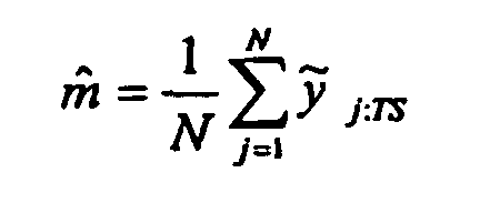
- a DC estimation unit 260 an estimation of m and is performed by using the received data determined to be the training sequence located in the received data generated by the training sequence, i.e., the estimate m and is generated according to where, is the j :th received signal generated by the pilot symbols (assuming there are N + L pilot symbols in each burst).
- the estimate of the DC-offset is performed by using N pilot symbols from the training sequence in the burst.
- bias DC offset value is introduced by modulation and this value adds to the estimate of m and .
- the bias DC offset value is determined as follows:
- the bias DC offset value, R DC can not yet be computed since the channel H is still unknown.
- U TS is known since it is based upon the known training sequence.
- the channel estimate H and obtained in the channel estimator 240 is then fed into an equalizer 250.
- the equalizer can be of any type, for example, an MLSE equalizer.
- An MLSE equalizer hypothesizes a received signal for all possible transmitted data sequences and after comparing each of these with the actually received signal, chooses the hypothesized data sequence with the maximum probability of being transmitted.
- the metric to be minimized is where N is the number of information symbols in the burst.
- the metric used in the equalizer 250 will be the same as the metric commonly used in classical MLSE equalizers for signals with no DC component.
- the DC-offset component will not determine the minimum amount of noise (i.e., the noise floor) in the receiver.
- compensation can be performed to accommodate for magnitude changes (a DC step) in the DC level of a received signal.
- a DC step can occur in a received signal when, for example, a strong nearby interferer ramps up its output signal.
- the baseband signal of a received burst is stored in buffer 210 and also is sent to a synchronization unit 220.
- the synchronization unit 220 locates the training sequence within the received data burst and supplies this synchronization information to the channel estimator 240.
- the data sequence values are fed to an offset change detection unit 310.
- the change detection unit 310 determines where changes in the DC-offset have occurred within a received burst of data.
- the offset change detection unit 310 may comprise, for example, a differentiator 410 and a threshold detector 420.
- the differentiator 410 and threshold detector 420 work in tandem to determine any step change in the DC level of the received data burst.
- the threshold detector 420 determines if
- the estimated power is determined in the threshold detector 420.
- the predefined threshold is a peak voltage value chosen based upon the particular application.
- the threshold will be small. If, for example, the receiver requires high accuracy for an application, the threshold will be small. If, for example, the receiver requires high accuracy for an application, the threshold will be small. If, for example, the receiver requires high accuracy for an application, the threshold will be small. If, for example, the receiver requires high accuracy for an application, the threshold will be small. If
- the received sequence, y i together with position information (i.e., the time instants where DC steps are found) are both fed to the DC offset estimator 260 that estimates ( n + 1) DC offsets, m and k (where n is the number of detected DC changes in the burst).
- the control unit 320 ensures that the DC offset estimates are subtracted from the received burst, y i , in synchronism.
- Figure 5A illustrates a typical burst of data containing a training sequence surrounded by transmitted data. If at least one DC step does not occur during the received burst or during a transmitted training sequence, the DC offset is estimated in the manner described above with respect to Figure 2. If, however, a DC step 500 occurs over a data sequence in a burst as illustrated in Figure 5B (when compared to Figure 5A), a rough compensation is performed. For the signal to the left of the DC step 500, compensation is performed in the manner described above with respect to Figure 2. However, in order to compensate for the DC offset to the right of the DC step 500 in Figure 5B the DC offset is estimated, as follows: where B is the number of bits in the burst. The DC offset estimation is then subtracted from the received signal as follows This calculation will result in an uncompensated bias DC offset for this part of the received signal because no known signals (i.e. training sequence) can be used when estimating.
- the DC offset to the left of the DC step 510 is estimated according to the following equation: where N 1 is the point in the data where the DC step occurs.
- the DC level to the right of the DC step 510 is estimated according to the following equation: where N is end of the training sequence of the burst.
Landscapes
- Engineering & Computer Science (AREA)
- Power Engineering (AREA)
- Computer Networks & Wireless Communication (AREA)
- Signal Processing (AREA)
- Physics & Mathematics (AREA)
- Mathematical Physics (AREA)
- Digital Transmission Methods That Use Modulated Carrier Waves (AREA)
- Cable Transmission Systems, Equalization Of Radio And Reduction Of Echo (AREA)
- Circuits Of Receivers In General (AREA)
- Amplifiers (AREA)
- Transmitters (AREA)
Abstract
Description
- The present invention generally relates to a method and apparatus for compensating for DC-offset when receiving signals in a radio receiver. More specifically, the present invention proposes a method and apparatus for compensating for DC-offset introduced in the radio receiver in.such a way that the DC-offset estimation and channel estimation are separated, and that any bias in the DC-offset estimation due to the transmitted symbols is compensated for in a channel estimator and in an equalizer.
- In digital communications systems, transmission signals are produced by the modulation of a carrier signal with digital data to be transmitted. The digital data is commonly transmitted in bursts where each burst consists of a number of data bits. When the transmitted signal is received, the signal requires demodulation in order to recover the data.
- Radio receiver architectures commonly employ direct conversion (i.e., homodyne) receivers to perform the demodulation of a received signal. A local oscillator operating at the carrier frequency is used to mix down the received signal to produce in-phase (I) and quadrature (Q) baseband signals. Direct conversion receivers are very efficient in terms of both cost and current consumption. The motivation behind the direct conversion receiver is to have the incoming carrier directly converted down to baseband, in both I and Q components, without use of any IF frequencies. However, direct conversion receivers also have drawbacks. For example, a DC-offset can be introduced to the DC level of received signal. A DC-offset arises from mainly three sources: (1) transistor mismatch in the signal path, (2) local oscillator signal leaking and self-downconverting to DC through the mixer, and (3) a large near-channel interferer leaking into the local oscillator and self-downconverting to DC. As a result, a signal that is received from a transmitter can be further distorted, and thereby lead to inaccurate data decoding. Additionally, the DC-offset can be several decibels (dB) larger than the information signal, requiring the DC-offset to be compensated for in order to be able to recover the transmitted data in the decoder.
- WO 98/25351 discloses a method for calculating an impulse response in a receiver, whereby the impulse response is calculated prior to any DC-offset being removed.
- The simple and most immediate way to compensate for the DC-offset is to estimate the mean value of the received burst, subtract the estimate from the received signal and then feed the signal to the decoder. GB 2,267,629 discloses such a system. However, the estimate introduces a bias DC offset, due to the finite amount of data used for estimating the DC-offset. The bias DC offset can be so large that the bit error rate of the receiver does not decrease as the signal-to-noise ratio increases. As a result, the bias DC offset will determine the minimum amount of noise (i.e., the noise floor) that is combined with the data within the receiver.
- Furthermore, since the transmitted data is unknown, it is impossible to compensate for the bias DC offset in the signal before it is supplied to the decoder unless a large amount of data is received (in which the bias DC offset will be reduced to zero) or both the transmitted symbols and the channel are known. A way to overcome this problem is to compensate the DC level in the decoder. However, while this solves the bias DC offset problem, the dynamics in the decoder will be too large because the DC-offset level can be several decibels (dB) larger than the received signal. Also, numerical problems are encountered when estimating the radio channel and the DC-offset simultaneously because of the magnitude difference between the channel parameters and the DC component. Therefore, there is a need for methods and apparatuses that separate the mean value estimation and channel estimation tasks and that also compensate for the bias DC offset introduced by the transmitted sequence.
- To remedy the problems encountered in conventional DC-offset compensation techniques, the present invention provides the ability to separate mean value estimation and channel estimation and the ability to compensate for bias DC offset introduced by the transmitted sequence.
- In according with one aspect of the present invention, there is provided a method for compensating for DC-offset in a receiver comprising the steps of: receiving a transmitted signal burst at said receiver; downconverting said signal burst into a first set of baseband component values; finding a known training sequence in the first set of baseband component values; characterised by the steps of: estimating a DC-offset value using said known training sequence; subtracting said DC-offset value from said first set of baseband component values to obtain a second set of baseband component values; performing channel estimation using said second set of baseband component values and outputting a channel model and a bias DC-offset value, and performing equalization of said second set of baseband component values using said second set of baseband component values, said estimated channel model and said bias DC offset value.
- Additionally, in accordance with another aspect of the present invention, there is provided an apparatus for compensating for DC-offset in a receiver comprising: means for receiving a transmitted signal burst at said receiver; means for downconverting said signal burst into a first set of baseband component values; means for locating a known training sequence in the first set of baseband component values; characterised by: means for estimating a DC-offset value using said known training sequence; means for subtracting said DC-offset value from said first set of baseband component values to obtain a second set of baseband component values; means for performing channel estimation using said second set of baseband component values and outputting a channel model and a bias DC-offset value, and means for performing equalization of said second set of baseband component values using said second set of baseband component values, said estimated channel model and said bias DC-offset value.
- These and other features, objects and advantages associated with the present invention will be more readily understood upon reading the following detailed description, in conjunction with the drawings in which like reference numerals refer to like elements and where:
- Figure 1 is a schematic diagram of a homodyne receiver which can be employed within cellular communications systems;
- Figure 2 is a block diagram of a DC-offset compensation device in accordance with an exemplary embodiment of the present invention;
- Figure 3 is a block diagram of a DC-offset compensation device to account for changing DC-offsets in accordance with an exemplary embodiment of the present invention;
- Figure 4 is a block diagram of a offset change detection unit in accordance with an exemplary embodiment of the present invention; and
- Figures 5A, 5B and 5C are diagrams of a typical TDMA burst, and DC steps that occur during a data sequence and during a training sequence of a typical TDMA burst in accordance with an exemplary embodiment of the present invention.
-
- The present invention will now be described with reference to the accompanying drawings, in which various exemplary embodiments of the invention are shown. However, this invention may be embodied in many different forms and should not be construed as limited to the specific embodiments shown. For example, while the present invention is described in a time division multiple access (TDMA) environment utilizing homodyne receivers, it could also be employed in other access environments and with other types of receivers where any type of channel estimator and equalization method can be used in digital communication.
- Figure 1 depicts a conventional
homodyne receiver 100 which can be employed within mobile communication systems to receive data bursts. As illustrated in Figure 1,antenna 105 receives a burst of data and sends the received burst tofirst filter 110. Thefirst filter 110 can be a bandpass filter which is designed to pass only the desired frequency band (for example, the GSM frequency band). Once filtered, the signal is sent to afirst amplifier 120. The first amplifier can be a low noise amplifier. The signal is then down converted to baseband in-phase (I) and quadrature phase (Q) signals by means of respective first andsecond mixers second mixers local oscillator 175. A first output of thelocal oscillator 175 is coupled to an output of thefirst mixer 130, and a second output of thelocal oscillator 175, having the same frequency and 90 degrees out of phase with the first output, is coupled to thesecond mixer 160. Thelocal oscillator 175 is set to the carrier frequency of the wanted signal. - The signals output from the first and
second mixers filters Filters D converters digital converters respective filters filters signal processor 190 for signal processing and recovery of the transmitted information. - Figure 2 shows a block diagram of a DC-
offset compensation apparatus 200 in accordance with an exemplary embodiment of the present invention. The DC-offset compensation apparatus 200 is located in thesignal processor 190 of Figure 1, and is employed to compensate for DC-offset introduced by the receiver. - The input baseband signal at time i,, which consists of B data in a burst can be written as follows:
 where y i is the desired information sequence, Ii + jQi, and m is the unknown DC-offset. The information sequence at time i can be written as follows:
U = [d i , d i-1,...,d i-L ] is a vector of transmitted symbols, and ei represents noise.
The received signalis stored in
buffer 210, where the in-phase and quadrature quantities can be stored separately. The received signalis also sent to a
synchronization unit 220. Synchronization information can be determined by correlating the received data stream to a training sequence, d i:TS , known to be included in the burst. In determining synchronization information, thesynchronization unit 220 finds the best match between the training sequence and the received signal and determines the position of the received samples in the burst that represent the training sequence. - In addition to determining synchronization information for later use by a channel estimator, the
synchronization unit 260 sends the received values to aDC estimation unit 260. At theDC estimation unit 260, an estimation of m and is performed by using the received data determined to be the training sequence located in the received data generated by the training sequence, i.e., the estimate m and is generated according towhere, is the j:th received signal generated by the pilot symbols (assuming there are N + L pilot symbols in each burst). In other words, the estimate of the DC-offset is performed by using N pilot symbols from the training sequence in the burst. By expanding m and, the estimate can be written as follows:
 where U j:TS = [d j:TS ,...,d j-L:TS ] T is the j:th vector of length L + 1 which only consists of pilot symbols d j:TS ,(i.e., known data).
- As discussed above, a bias DC offset value is introduced by modulation and this value adds to the estimate of m and. The bias DC offset value is determined as follows:The bias DC offset value, RDC, can not yet be computed since the channel H is still unknown. However,

U TS is known since it is based upon the known training sequence. By subtracting the estimated mean value determined in the DC-offsetestimation unit 260 from the received input sequence stored inbuffer 210 atadder 230, the following result is obtained:The signal y and i together with synchronization information determined in the
synchronization unit 220 are fed to achannel estimator 240 where y and j:TS , j=1,...,N is used for estimating the channel and y and j:TS can be written as follows:As can be seen from equation (7), it is possible to use the following model in the channel estimator:

- The difference between the model used in the
channel estimator 240 in accordance with an exemplary embodiment of the present invention and the classical channel model, is that the input sequence U j:TS -U TS is used instead of U j:TS , thereby compensating for the bias DC offset introduced by the modulation. Furthermore, note that this will be the best compensation able to be performed since in the noise free case (i.e., Var(e i ) = 0) equations (7) and (8) are perfectly matched, thereby indicating that H and → H when Var(e i ) → 0. Thus, in the noise free case perfect channel estimates can be obtained. - The channel estimate H and obtained in the
channel estimator 240 is then fed into anequalizer 250. The equalizer can be of any type, for example, an MLSE equalizer. An MLSE equalizer hypothesizes a received signal for all possible transmitted data sequences and after comparing each of these with the actually received signal, chooses the hypothesized data sequence with the maximum probability of being transmitted. The metric used in the equalizer includes the term R and DC = H and TU TS . The metric to be minimized iswhere N is the number of information symbols in the burst. As can be seen from (7) and (9), by including the extra term R and DC = H and T
U TS as shown in equation (9), the metric used in theequalizer 250 will be the same as the metric commonly used in classical MLSE equalizers for signals with no DC component. Thus, by using thechannel estimator 240 andequalizer 250 presented above, the DC-offset component will not determine the minimum amount of noise (i.e., the noise floor) in the receiver. - In accordance with another exemplary embodiment of the present invention, compensation can be performed to accommodate for magnitude changes (a DC step) in the DC level of a received signal. A DC step can occur in a received signal when, for example, a strong nearby interferer ramps up its output signal. In the DC offset
compensation apparatus 300 illustrated in Figure 3, the baseband signal of a received burst is stored inbuffer 210 and also is sent to asynchronization unit 220. Thesynchronization unit 220 locates the training sequence within the received data burst and supplies this synchronization information to thechannel estimator 240. The data sequence values are fed to an offsetchange detection unit 310. Thechange detection unit 310 determines where changes in the DC-offset have occurred within a received burst of data. - As illustrated in Figure 4, the offset
change detection unit 310 may comprise, for example, adifferentiator 410 and athreshold detector 420. Thedifferentiator 410 andthreshold detector 420 work in tandem to determine any step change in the DC level of the received data burst. Thedifferentiator 410 differentiates the received signal (e.g., let x i =- .). Next, the
threshold detector 420 determines if |x i |/Pow(y i ) > α, where Pow() is the estimated power of y i , and α is a predefined threshold. The estimated power is determined in the
threshold detector 420. The predefined threshold is a peak voltage value chosen based upon the particular application. If, for example, the receiver requires high accuracy for an application, the threshold will be small. If |x i |/Pow(y i ) is greater than α, then a DC step is determined to have.occurred at position i. Alternatively, the signal x i can be low pass filtered rather than being differentiated by a differentiator, before being compared to the predetermined threshold. - Referring back now to Figure 3, the received sequence, y i , together with position information (i.e., the time instants where DC steps are found) are both fed to the DC offset
estimator 260 that estimates (n + 1) DC offsets, m and k (where n is the number of detected DC changes in the burst). The estimated DC offsets m and k , where k = 1, ..., n + 1, are fed to acontrol unit 320. Thecontrol unit 320 ensures that the DC offset estimates are subtracted from the received burst,y i , in synchronism. - Figure 5A illustrates a typical burst of data containing a training sequence surrounded by transmitted data. If at least one DC step does not occur during the received burst or during a transmitted training sequence, the DC offset is estimated in the manner described above with respect to Figure 2. If, however, a
DC step 500 occurs over a data sequence in a burst as illustrated in Figure 5B (when compared to Figure 5A), a rough compensation is performed. For the signal to the left of theDC step 500, compensation is performed in the manner described above with respect to Figure 2. However, in order to compensate for the DC offset to the right of theDC step 500 in Figure 5B the DC offset is estimated, as follows:where B is the number of bits in the burst. The DC offset estimation is then subtracted from the received signal as follows This calculation will result in an uncompensated bias DC offset for this part of the received signal because no known signals (i.e. training sequence) can be used when estimating.
- In another example as illustrated in Figure 5C, if a DC step occurs somewhere within the training sequence, the DC offset to the left of the
DC step 510 is estimated according to the following equation:where N1 is the point in the data where the DC step occurs. The DC level to the right of the
DC step 510 is estimated according to the following equation:where N is end of the training sequence of the burst. Thus, each half burst is treated independently and a correction value is determined in the same way as described above for each half burst (m and 1, m and 2), and subtracted, and the residual DC for each burst is compensated for in the
channel estimator 240 andequalizer 250. - In this case the model used in the
channel estimator 240 is as follows:where
U j:TS =U 1:N1 -1.TS , j = 1, ... N 1 - 1 is the mean value vector of the training sequence fromtime 1 to N 1, - 1 andU j:TS =U N1 :N.TS , j = N 1, ..., N is the mean value vector of the training sequence from time N 1 to N. - While the present invention has been described with respect to its preferred embodiment, those skilled in the art will recognize that the present invention is not limited to the specific embodiment described and illustrated herein. Different embodiments and adaptations besides those shown herein and described as well as many variations, modifications and equivalent arrangements will now be apparent or will be reasonably suggested by the foregoing specification and drawings without departing from the substance of the scope of the invention.
Claims (20)
- A method for compensating for DC-offset in a receiver comprising the steps of:receiving a transmitted signal burst at said receiver;downconverting said signal burst into a first set of baseband component values;finding a known training sequence in first the set of baseband component values; characterised by the steps of:estimating a DC-offset value using said known training sequence;subtracting said DC-offset value from said first set of baseband component values to obtain a second set of baseband component values;performing channel estimation using said second set of baseband component values and outputting a channel model and a bias DC-offset value, andperforming equalization of said second set of baseband component values using said second set of baseband component values, said estimated channel model and said bias DC-offset value.
- The method of claim 1, wherein said first set of baseband component values are digitized signals.
- The method of claim 1, wherein said first set of baseband component values are in-phase and quadrature components of said received signal.
- The method of claim 1, wherein said known training sequence comprises N pilot symbols, and said DC-offset value estimation is performed according to the following equation:where,
 is a j:th vector of L+1 of the pilot symbols and L is the number of corresponding taps.
- The method of claim 1, wherein said bias DC-offset value is determined according to the following equation:where H is a channel model, U is a reference training sequence, and N is the number of pilot symbols from the training sequence.

- The method of claim 1, after said finding step, further comprising the step of:determining the location of at least one DC step value within said received baseband signal.
- The method of claim 6, wherein said determining step further comprises:differentiating said first set of baseband component values; anddetermining whether the differentiated baseband component values exceed a predetermined threshold value.
- The method of claim 6, wherein said subtracting step further comprises:controlling the subtraction of said DC offset estimates from said received signal to ensure data synchronism between the estimated DC offset values and said first set of baseband components.
- The method of claim 6, wherein if said DC step occurs within a training sequence of said transmitted sequence, the estimating step is performed independently over a part of the received message affected by said DC step and over a part of the message not affected by the DC step.
- The method of claim 6, wherein if a DC step does not occur over a training sequence of said received burst, said DC offset value estimation over the DC step is performed according to the following equation:where B is the number of bits in a burst, i 0 is the time of occurrence of the DC step and where
 is the kth vector of the received burst.
- An apparatus for compensating for DC-offset in a receiver comprising:means for receiving a transmitted signal burst at said receiver;means for downconverting said signal burst into a first set of baseband component values;means (220) for locating a known training sequence in the first set of baseband component values; characterised by:means (260) for estimating a DC-offset value using said known training sequence;means (230) for subtracting said DC-offset value from said first set of baseband component values to obtain a second set of baseband component values;means (240) for performing channel estimation using said second set of baseband component values and outputting a channel model and a bias DC-offset value, andmeans (250) for performing equalization of said second set of baseband component values using said second set of baseband component values, said estimated channel model and said bias DC-offset value.
- The apparatus of claim 11, wherein said first set of baseband signal components are digital signals.
- The apparatus of claim 11, wherein said first set of baseband component values are in-phase and quadrature components of said received signal.
- The apparatus of claim 11, wherein said known training sequence comprises N pilot symbols, and the means for estimating the DC-offset value is adapted to determine the DC offset value according to the following equation:where
 is a j:th vector of L+1 of the pilot symbols, and where L is the number of corresponding taps.
- The apparatus of claim 11, wherein said means for performing channel estimation is adapted to determine said bias DC-offset value according to the following equation:where H is a channel model, U is a reference training sequence, and N is the number of pilot symbols from the training sequence.

- The apparatus of claim 11, further comprising:means (310) for determining the location of at least one DC step value within said received baseband signal.
- The apparatus of claim 16, wherein said means for determining further comprises:means (410) for differentiating said first baseband component values; andmeans (420) for determining whether the differentiated baseband component values exceed a predetermined threshold value.
- The apparatus of claim 16, further comprising:means for controlling the subtraction of said DC offset estimates from said received signal to ensure data synchronism between the estimated DC offset values and said first set of baseband components.
- The apparatus of claim 16, wherein the means for estimating a DC-offset value is configured such that, if a DC step occurs within a training sequence of said transmitted sequence, an estimating step is performed independently over a part of the received message affected by the DC step and over a part of the message not affected by the DC step.
- The apparatus of claim 16, wherein the means for estimating a DC-offset value is configured such that, if a DC step does not occur over a training sequence of said received burst, said DC-offset value estimation over the DC step is performed according to the following equation:where B is the number of bits in a burst, i 0 is the time of occurrence of the DC step and y and k is the kth vector of the received burst.

Applications Claiming Priority (3)
| Application Number | Priority Date | Filing Date | Title |
|---|---|---|---|
| US347020 | 1999-07-02 | ||
| US09/347,020 US6370205B1 (en) | 1999-07-02 | 1999-07-02 | Method and apparatus for performing DC-offset compensation in a radio receiver |
| PCT/EP2000/005756 WO2001003395A1 (en) | 1999-07-02 | 2000-06-21 | A method and apparatus for performing dc-offset compensation in a radio receiver |
Publications (2)
| Publication Number | Publication Date |
|---|---|
| EP1197049A1 EP1197049A1 (en) | 2002-04-17 |
| EP1197049B1 true EP1197049B1 (en) | 2005-08-24 |
Family
ID=23361997
Family Applications (1)
| Application Number | Title | Priority Date | Filing Date |
|---|---|---|---|
| EP00943857A Expired - Lifetime EP1197049B1 (en) | 1999-07-02 | 2000-06-21 | A method and apparatus for performing dc-offset compensation in a radio receiver |
Country Status (9)
| Country | Link |
|---|---|
| US (1) | US6370205B1 (en) |
| EP (1) | EP1197049B1 (en) |
| JP (1) | JP2003503960A (en) |
| CN (1) | CN1372743A (en) |
| AT (1) | ATE303031T1 (en) |
| AU (1) | AU5817900A (en) |
| DE (1) | DE60022198D1 (en) |
| MY (1) | MY120478A (en) |
| WO (1) | WO2001003395A1 (en) |
Families Citing this family (52)
| Publication number | Priority date | Publication date | Assignee | Title |
|---|---|---|---|---|
| AUPP261898A0 (en) * | 1998-03-27 | 1998-04-23 | Victoria University Of Technology | Dc offset and im2 removal in direct conversion receivers |
| SE9900289D0 (en) * | 1999-01-27 | 1999-01-27 | Ericsson Telefon Ab L M | DC estimate method for a homodyne receiver |
| WO2000072441A1 (en) * | 1999-05-24 | 2000-11-30 | Level One Communications, Inc. | Automatic gain control and offset correction |
| US6449320B1 (en) * | 1999-07-02 | 2002-09-10 | Telefonaktiebolaget Lm Ericsson (Publ) | Equalization with DC-offset compensation |
| WO2001031867A1 (en) * | 1999-10-27 | 2001-05-03 | Nokia Corporation | Dc offset correction in a mobile communication system |
| US6985541B1 (en) | 1999-11-23 | 2006-01-10 | Micor Linear Corporation | FM demodulator for a low IF receiver |
| US7076217B1 (en) | 1999-11-23 | 2006-07-11 | Micro Linear Corporation | Integrated radio transceiver |
| US7027792B1 (en) | 1999-11-23 | 2006-04-11 | Micro Linear Corporation | Topology for a single ended input dual balanced mixer |
| US6987816B1 (en) * | 1999-11-23 | 2006-01-17 | Micro Linear Corporation | Iris data recovery algorithms |
| US6628706B1 (en) * | 1999-12-06 | 2003-09-30 | Telefonaktiebolaget Lm Ericsson (Publ) | Method and apparatus for transforming a channel estimate |
| GB2366460A (en) * | 2000-08-24 | 2002-03-06 | Nokia Mobile Phones Ltd | DC compensation for a direct conversion radio receiver |
| DE10043743A1 (en) * | 2000-09-05 | 2002-03-14 | Infineon Technologies Ag | Automatic frequency correction for mobile radio receivers |
| US7512109B2 (en) * | 2000-09-29 | 2009-03-31 | Intel Corporation | Slot structure for radio communications system |
| US7068987B2 (en) | 2000-10-02 | 2006-06-27 | Conexant, Inc. | Packet acquisition and channel tracking for a wireless communication device configured in a zero intermediate frequency architecture |
| US6977978B1 (en) * | 2000-10-02 | 2005-12-20 | Telefonaktiebolaget Lm Ericsson (Publ) | Adaptive channel filtration for communications systems |
| US6748200B1 (en) | 2000-10-02 | 2004-06-08 | Mark A. Webster | Automatic gain control system and method for a ZIF architecture |
| US6775340B1 (en) * | 2000-10-13 | 2004-08-10 | Ericsson Inc. | Synchronization and channel estimation with extended pilot symbols |
| US6725024B1 (en) * | 2000-11-07 | 2004-04-20 | Telefonaktiebolaget Lm Ericsson (Publ) | Offset local oscillator frequency |
| US6901121B1 (en) | 2001-02-20 | 2005-05-31 | Comsys Communication & Signal Processing Ltd. | Compensation of DC offset impairment in a communications receiver |
| US6977977B1 (en) | 2001-02-20 | 2005-12-20 | Comsys Communication & Signal Processing Ltd. | Compensation of I/Q gain mismatch in a communications receiver |
| FR2821218B1 (en) * | 2001-02-22 | 2006-06-23 | Cit Alcatel | RECEPTION DEVICE FOR A MOBILE RADIOCOMMUNICATION TERMINAL |
| US7231000B2 (en) * | 2001-10-22 | 2007-06-12 | Broadcom Corporation | System and method for DC offset compensation and bit synchronization |
| KR100436207B1 (en) * | 2002-06-18 | 2004-06-12 | 전자부품연구원 | Homerf system using channel estimation and dc offset compensation |
| US7190740B2 (en) * | 2002-08-19 | 2007-03-13 | Siemens Communications, Inc. | Arrangement for dynamic DC offset compensation |
| EP1422894B1 (en) * | 2002-11-20 | 2015-04-29 | TELEFONAKTIEBOLAGET LM ERICSSON (publ) | Method and corresponding arrangement for DC offset compensation using channel estimation |
| JP4414342B2 (en) * | 2002-11-20 | 2010-02-10 | テレフオンアクチーボラゲット エル エム エリクソン(パブル) | Method and apparatus for DC offset compensation using channel estimation |
| AU2003289425A1 (en) | 2002-12-20 | 2004-07-14 | Renesas Technology Corp. | Transmission circuit and transmitter/receiver using same |
| TWI256220B (en) * | 2003-04-17 | 2006-06-01 | United Radiotek Inc | Digital dc bias estimation apparatus and method |
| SE526872C2 (en) * | 2003-05-26 | 2005-11-15 | Infineon Technologies Wireless | Method and arrangement for removing DC offset from data symbols |
| JP2004362065A (en) | 2003-06-02 | 2004-12-24 | Denso Corp | Map information retrieval system, method and program |
| US6998908B1 (en) * | 2003-06-10 | 2006-02-14 | Rockwell Collins, Inc. | Adaptive interference cancellation receiving system using synthesizer phase accumulation |
| US7330320B1 (en) * | 2003-06-16 | 2008-02-12 | Marvell International Ltd. | Method and apparatus to limit DC-level in coded data |
| US7623596B2 (en) * | 2003-06-27 | 2009-11-24 | Ericsson, Inc. | Methods and systems for estimating a channel response by applying bias to an initial channel estimate |
| SE0302156D0 (en) * | 2003-08-01 | 2003-08-01 | Infineon Technologies Ag | Low-latency DC compensation |
| US7266160B2 (en) | 2003-10-20 | 2007-09-04 | Analog Devices, Inc. | Method for joint DC offset correction and channel coefficient estimation in a receiver |
| US7583765B2 (en) * | 2005-04-26 | 2009-09-01 | Skyworks Solutions, Inc. | DC offset detection and cancellation in a receiver |
| WO2007003979A1 (en) * | 2005-07-01 | 2007-01-11 | Telefonaktiebolaget Lm Ericsson (Publ) | Method and arrangement for estimating dc offset |
| US20070030095A1 (en) * | 2005-08-05 | 2007-02-08 | Mitsutaka Hikita | Antenna duplexer and wireless terminal using the same |
| US7622987B1 (en) | 2007-01-25 | 2009-11-24 | Pmc-Sierra, Inc. | Pattern-based DC offset correction |
| JP2008300958A (en) * | 2007-05-29 | 2008-12-11 | Panasonic Corp | Dynamic dc-offset canceling apparatus and dynamic dc offset canceling method |
| US20090122928A1 (en) * | 2007-11-13 | 2009-05-14 | Horizon Semiconductors Ltd. | Apparatus and method for frequency estimation in the presence of narrowband gaussian noise |
| GB0803710D0 (en) * | 2008-02-28 | 2008-04-09 | Nokia Corp | DC compensation |
| US8855580B2 (en) * | 2008-06-27 | 2014-10-07 | Telefonaktiebolaget L M Ericsson (Publ) | Methods and apparatus for reducing own-transmitter interference in low-IF and zero-IF receivers |
| US7995973B2 (en) * | 2008-12-19 | 2011-08-09 | Telefonaktiebolaget Lm Ericsson (Publ) | Own transmitter interference tolerant transceiver and receiving methods |
| US8055234B2 (en) * | 2008-06-27 | 2011-11-08 | Telefonaktiebolaget Lm Ericsson (Publ) | Methods and apparatus for suppressing strong-signal interference in low-IF receivers |
| US8027651B2 (en) * | 2008-12-05 | 2011-09-27 | Motorola Solutions, Inc. | Method and apparatus for removing DC offset in a direct conversion receiver |
| US8090320B2 (en) * | 2008-12-19 | 2012-01-03 | Telefonaktiebolaget Lm Ericsson (Publ) | Strong signal tolerant OFDM receiver and receiving methods |
| CN101938283B (en) * | 2009-06-29 | 2013-09-04 | 国基电子(上海)有限公司 | Multi-carrier interference eliminating circuit and a signal receiving and transmitting system using same |
| US8565351B2 (en) * | 2011-04-28 | 2013-10-22 | Mediatek Singapore Pte. Ltd. | Channel impulse response (CIR)/DC offset (DCO) joint estimation block and method |
| EP2941852A1 (en) * | 2013-01-03 | 2015-11-11 | Huawei Technologies Co., Ltd. | Method for estimating and removing dc offset |
| US8942316B2 (en) | 2013-03-15 | 2015-01-27 | Samsung Electronics Co., Ltd. | Wireless communication system with signal processing mechanism and method of operation thereof |
| GB201907717D0 (en) * | 2019-05-31 | 2019-07-17 | Nordic Semiconductor Asa | Apparatus and methods for dc-offset estimation |
Family Cites Families (20)
| Publication number | Priority date | Publication date | Assignee | Title |
|---|---|---|---|---|
| JP2538963B2 (en) | 1987-12-26 | 1996-10-02 | 株式会社東芝 | Waveform equalizer |
| US4873702A (en) | 1988-10-20 | 1989-10-10 | Chiu Ran Fun | Method and apparatus for DC restoration in digital receivers |
| US4887050A (en) * | 1989-03-31 | 1989-12-12 | Motorola, Inc. | Frequency control apparatus and method for a digital radio receiver |
| JPH04103222A (en) | 1990-08-22 | 1992-04-06 | Nec Home Electron Ltd | Analog/digital converter |
| US5241702A (en) | 1990-09-06 | 1993-08-31 | Telefonaktiebolaget L M Ericsson | D.c. offset compensation in a radio receiver |
| GB2267629B (en) | 1992-06-03 | 1995-10-25 | Fujitsu Ltd | Signal error reduction in receiving apparatus |
| GB9211712D0 (en) | 1992-06-03 | 1992-07-15 | Fujitsu Microelectronics Ltd | Gm digital receive processing |
| JP3084952B2 (en) | 1992-09-07 | 2000-09-04 | 松下電器産業株式会社 | Data decoding device |
| US5319679A (en) | 1992-12-09 | 1994-06-07 | Datum Systems | Method and apparatus for recovering data from a radio signal |
| GB2274759B (en) | 1993-02-02 | 1996-11-13 | Nokia Mobile Phones Ltd | Correction of D.C offset in received and demodulated radio signals |
| JPH07297869A (en) | 1994-04-25 | 1995-11-10 | Matsushita Electric Ind Co Ltd | Receiver |
| US5724653A (en) * | 1994-12-20 | 1998-03-03 | Lucent Technologies Inc. | Radio receiver with DC offset correction circuit |
| JPH08237317A (en) | 1995-02-28 | 1996-09-13 | Fujitsu Ltd | Demodulation circuit and receiver |
| US5748681A (en) * | 1995-10-27 | 1998-05-05 | Lucent Technologies Inc | Offset correction for a homodyne radio |
| FI962140A (en) * | 1996-05-21 | 1997-11-22 | Nokia Telecommunications Oy | Method for estimating impulse response and receiver |
| JPH09331257A (en) | 1996-06-11 | 1997-12-22 | Kokusai Electric Co Ltd | Dc offset canceling circuit |
| EP0876719B1 (en) * | 1996-11-13 | 2005-03-16 | Nokia Corporation | Method, transmitter and receiver for transmitting training signals in a tdma transmission system |
| FI101919B1 (en) | 1996-11-21 | 1998-09-15 | Nokia Telecommunications Oy | Method for calculating impulse response and receiver |
| JP3652039B2 (en) | 1996-12-04 | 2005-05-25 | 松下電器産業株式会社 | Data receiving device |
| KR100268449B1 (en) * | 1998-06-25 | 2000-10-16 | 윤종용 | System with improved base band-analog circuit |
-
1999
- 1999-07-02 US US09/347,020 patent/US6370205B1/en not_active Expired - Fee Related
-
2000
- 2000-06-21 EP EP00943857A patent/EP1197049B1/en not_active Expired - Lifetime
- 2000-06-21 AT AT00943857T patent/ATE303031T1/en not_active IP Right Cessation
- 2000-06-21 DE DE60022198T patent/DE60022198D1/en not_active Expired - Lifetime
- 2000-06-21 AU AU58179/00A patent/AU5817900A/en not_active Abandoned
- 2000-06-21 CN CN00812387.XA patent/CN1372743A/en active Pending
- 2000-06-21 WO PCT/EP2000/005756 patent/WO2001003395A1/en active IP Right Grant
- 2000-06-21 JP JP2001508133A patent/JP2003503960A/en not_active Withdrawn
- 2000-06-27 MY MYPI20002898A patent/MY120478A/en unknown
Also Published As
| Publication number | Publication date |
|---|---|
| EP1197049A1 (en) | 2002-04-17 |
| ATE303031T1 (en) | 2005-09-15 |
| WO2001003395A1 (en) | 2001-01-11 |
| JP2003503960A (en) | 2003-01-28 |
| AU5817900A (en) | 2001-01-22 |
| US6370205B1 (en) | 2002-04-09 |
| CN1372743A (en) | 2002-10-02 |
| MY120478A (en) | 2005-10-31 |
| DE60022198D1 (en) | 2005-09-29 |
Similar Documents
| Publication | Publication Date | Title |
|---|---|---|
| EP1197049B1 (en) | A method and apparatus for performing dc-offset compensation in a radio receiver | |
| EP1195033B1 (en) | Equalization with dc-offset compensation | |
| EP0563300B1 (en) | Apparatus and method for equalizing a corrupted signal in a receiver | |
| KR101054626B1 (en) | Modulation Type Detection | |
| EP1228611B1 (en) | Radio receiver with two stages of dc offset correction, synchronisation and channel estimation | |
| US6408023B1 (en) | Method and apparatus for performing equalization in a radio receiver | |
| US7301993B2 (en) | Channel estimation in a spread spectrum receiver | |
| US6628926B1 (en) | Method for automatic frequency control | |
| US7269234B2 (en) | Arrangement for dynamic DC offset compensation | |
| US6269131B1 (en) | Physical channel estimator | |
| JP2002000023U (en) | Receiver including frequency deviation evaluator | |
| US20070217550A1 (en) | System having a signal processor for detection of a signal type | |
| US7664210B2 (en) | Non-coherent synchronous direct-conversion receiving apparatus for compensating frequency offset | |
| US6934346B2 (en) | Apparatus and method for substantially eliminating a near-channel interfering amplitude modulated signal | |
| JP2005507570A (en) | Automatic frequency control system and combined demodulation method | |
| EP0883949B1 (en) | Channel estimation arrangement | |
| US6618453B1 (en) | Estimating interference in a communication system | |
| GB2287620A (en) | A Digital cellular mobile radio receiver | |
| EP1130866A1 (en) | Correction of quadrature and gain errors in homodyne receivers | |
| EP1337083A1 (en) | DC offset and channel impulse response estimation | |
| EP1466455B1 (en) | Frequency error estimation | |
| US7257180B2 (en) | Method for receiving a message signal, receiver, receiving device and message transmission system for this | |
| KR100978703B1 (en) | Method and apparatus for dc offset compensation in a digital communication system | |
| EP1061667A1 (en) | Improved channel estimation technique | |
| KR100480691B1 (en) | (apparatus for interfacing in broadcast receiving system's demodulator and decoder |
Legal Events
| Date | Code | Title | Description |
|---|---|---|---|
| PUAI | Public reference made under article 153(3) epc to a published international application that has entered the european phase |
Free format text: ORIGINAL CODE: 0009012 |
|
| 17P | Request for examination filed |
Effective date: 20020128 |
|
| AK | Designated contracting states |
Kind code of ref document: A1 Designated state(s): AT BE CH CY DE DK ES FI FR GB GR IE IT LI LU MC NL PT SE |
|
| AX | Request for extension of the european patent |
Free format text: AL;LT;LV;MK;RO;SI |
|
| RAP1 | Party data changed (applicant data changed or rights of an application transferred) |
Owner name: TELEFONAKTIEBOLAGET LM ERICSSON (PUBL) |
|
| 17Q | First examination report despatched |
Effective date: 20040611 |
|
| GRAP | Despatch of communication of intention to grant a patent |
Free format text: ORIGINAL CODE: EPIDOSNIGR1 |
|
| GRAS | Grant fee paid |
Free format text: ORIGINAL CODE: EPIDOSNIGR3 |
|
| GRAA | (expected) grant |
Free format text: ORIGINAL CODE: 0009210 |
|
| AK | Designated contracting states |
Kind code of ref document: B1 Designated state(s): AT BE CH CY DE DK ES FI FR GB GR IE IT LI LU MC NL PT SE |
|
| PG25 | Lapsed in a contracting state [announced via postgrant information from national office to epo] |
Ref country code: IT Free format text: LAPSE BECAUSE OF FAILURE TO SUBMIT A TRANSLATION OF THE DESCRIPTION OR TO PAY THE FEE WITHIN THE PRESCRIBED TIME-LIMIT;WARNING: LAPSES OF ITALIAN PATENTS WITH EFFECTIVE DATE BEFORE 2007 MAY HAVE OCCURRED AT ANY TIME BEFORE 2007. THE CORRECT EFFECTIVE DATE MAY BE DIFFERENT FROM THE ONE RECORDED. Effective date: 20050824 Ref country code: CH Free format text: LAPSE BECAUSE OF FAILURE TO SUBMIT A TRANSLATION OF THE DESCRIPTION OR TO PAY THE FEE WITHIN THE PRESCRIBED TIME-LIMIT Effective date: 20050824 Ref country code: FI Free format text: LAPSE BECAUSE OF FAILURE TO SUBMIT A TRANSLATION OF THE DESCRIPTION OR TO PAY THE FEE WITHIN THE PRESCRIBED TIME-LIMIT Effective date: 20050824 Ref country code: NL Free format text: LAPSE BECAUSE OF FAILURE TO SUBMIT A TRANSLATION OF THE DESCRIPTION OR TO PAY THE FEE WITHIN THE PRESCRIBED TIME-LIMIT Effective date: 20050824 Ref country code: AT Free format text: LAPSE BECAUSE OF FAILURE TO SUBMIT A TRANSLATION OF THE DESCRIPTION OR TO PAY THE FEE WITHIN THE PRESCRIBED TIME-LIMIT Effective date: 20050824 Ref country code: LI Free format text: LAPSE BECAUSE OF FAILURE TO SUBMIT A TRANSLATION OF THE DESCRIPTION OR TO PAY THE FEE WITHIN THE PRESCRIBED TIME-LIMIT Effective date: 20050824 Ref country code: BE Free format text: LAPSE BECAUSE OF FAILURE TO SUBMIT A TRANSLATION OF THE DESCRIPTION OR TO PAY THE FEE WITHIN THE PRESCRIBED TIME-LIMIT Effective date: 20050824 |
|
| REG | Reference to a national code |
Ref country code: GB Ref legal event code: FG4D |
|
| REG | Reference to a national code |
Ref country code: CH Ref legal event code: EP |
|
| REG | Reference to a national code |
Ref country code: IE Ref legal event code: FG4D |
|
| REF | Corresponds to: |
Ref document number: 60022198 Country of ref document: DE Date of ref document: 20050929 Kind code of ref document: P |
|
| PG25 | Lapsed in a contracting state [announced via postgrant information from national office to epo] |
Ref country code: SE Free format text: LAPSE BECAUSE OF FAILURE TO SUBMIT A TRANSLATION OF THE DESCRIPTION OR TO PAY THE FEE WITHIN THE PRESCRIBED TIME-LIMIT Effective date: 20051124 Ref country code: GR Free format text: LAPSE BECAUSE OF FAILURE TO SUBMIT A TRANSLATION OF THE DESCRIPTION OR TO PAY THE FEE WITHIN THE PRESCRIBED TIME-LIMIT Effective date: 20051124 Ref country code: DK Free format text: LAPSE BECAUSE OF FAILURE TO SUBMIT A TRANSLATION OF THE DESCRIPTION OR TO PAY THE FEE WITHIN THE PRESCRIBED TIME-LIMIT Effective date: 20051124 |
|
| PG25 | Lapsed in a contracting state [announced via postgrant information from national office to epo] |
Ref country code: DE Free format text: LAPSE BECAUSE OF FAILURE TO SUBMIT A TRANSLATION OF THE DESCRIPTION OR TO PAY THE FEE WITHIN THE PRESCRIBED TIME-LIMIT Effective date: 20051125 |
|
| PG25 | Lapsed in a contracting state [announced via postgrant information from national office to epo] |
Ref country code: ES Free format text: LAPSE BECAUSE OF FAILURE TO SUBMIT A TRANSLATION OF THE DESCRIPTION OR TO PAY THE FEE WITHIN THE PRESCRIBED TIME-LIMIT Effective date: 20051205 |
|
| PG25 | Lapsed in a contracting state [announced via postgrant information from national office to epo] |
Ref country code: PT Free format text: LAPSE BECAUSE OF FAILURE TO SUBMIT A TRANSLATION OF THE DESCRIPTION OR TO PAY THE FEE WITHIN THE PRESCRIBED TIME-LIMIT Effective date: 20060124 |
|
| NLV1 | Nl: lapsed or annulled due to failure to fulfill the requirements of art. 29p and 29m of the patents act | ||
| REG | Reference to a national code |
Ref country code: CH Ref legal event code: PL |
|
| PGFP | Annual fee paid to national office [announced via postgrant information from national office to epo] |
Ref country code: MC Payment date: 20060602 Year of fee payment: 7 |
|
| PGFP | Annual fee paid to national office [announced via postgrant information from national office to epo] |
Ref country code: FR Payment date: 20060620 Year of fee payment: 7 |
|
| PGFP | Annual fee paid to national office [announced via postgrant information from national office to epo] |
Ref country code: IE Payment date: 20060629 Year of fee payment: 7 |
|
| PGFP | Annual fee paid to national office [announced via postgrant information from national office to epo] |
Ref country code: LU Payment date: 20060630 Year of fee payment: 7 |
|
| PLBE | No opposition filed within time limit |
Free format text: ORIGINAL CODE: 0009261 |
|
| STAA | Information on the status of an ep patent application or granted ep patent |
Free format text: STATUS: NO OPPOSITION FILED WITHIN TIME LIMIT |
|
| 26N | No opposition filed |
Effective date: 20060526 |
|
| EN | Fr: translation not filed | ||
| PG25 | Lapsed in a contracting state [announced via postgrant information from national office to epo] |
Ref country code: FR Free format text: LAPSE BECAUSE OF FAILURE TO SUBMIT A TRANSLATION OF THE DESCRIPTION OR TO PAY THE FEE WITHIN THE PRESCRIBED TIME-LIMIT Effective date: 20061020 |
|
| PG25 | Lapsed in a contracting state [announced via postgrant information from national office to epo] |
Ref country code: MC Free format text: LAPSE BECAUSE OF NON-PAYMENT OF DUE FEES Effective date: 20070630 |
|
| REG | Reference to a national code |
Ref country code: IE Ref legal event code: MM4A |
|
| PG25 | Lapsed in a contracting state [announced via postgrant information from national office to epo] |
Ref country code: IE Free format text: LAPSE BECAUSE OF NON-PAYMENT OF DUE FEES Effective date: 20070621 |
|
| PG25 | Lapsed in a contracting state [announced via postgrant information from national office to epo] |
Ref country code: CY Free format text: LAPSE BECAUSE OF FAILURE TO SUBMIT A TRANSLATION OF THE DESCRIPTION OR TO PAY THE FEE WITHIN THE PRESCRIBED TIME-LIMIT Effective date: 20050824 |
|
| PGFP | Annual fee paid to national office [announced via postgrant information from national office to epo] |
Ref country code: GB Payment date: 20080627 Year of fee payment: 9 |
|
| PG25 | Lapsed in a contracting state [announced via postgrant information from national office to epo] |
Ref country code: LU Free format text: LAPSE BECAUSE OF NON-PAYMENT OF DUE FEES Effective date: 20070621 |
|
| GBPC | Gb: european patent ceased through non-payment of renewal fee |
Effective date: 20090621 |
|
| PG25 | Lapsed in a contracting state [announced via postgrant information from national office to epo] |
Ref country code: GB Free format text: LAPSE BECAUSE OF NON-PAYMENT OF DUE FEES Effective date: 20090621 |