EP1195905A1 - D/A-A/D method and arrangement for reducing interference - Google Patents
D/A-A/D method and arrangement for reducing interference Download PDFInfo
- Publication number
- EP1195905A1 EP1195905A1 EP01000368A EP01000368A EP1195905A1 EP 1195905 A1 EP1195905 A1 EP 1195905A1 EP 01000368 A EP01000368 A EP 01000368A EP 01000368 A EP01000368 A EP 01000368A EP 1195905 A1 EP1195905 A1 EP 1195905A1
- Authority
- EP
- European Patent Office
- Prior art keywords
- signal
- serial
- converter
- clock signal
- frequency
- Prior art date
- Legal status (The legal status is an assumption and is not a legal conclusion. Google has not performed a legal analysis and makes no representation as to the accuracy of the status listed.)
- Withdrawn
Links
Images

Classifications
-
- H—ELECTRICITY
- H04—ELECTRIC COMMUNICATION TECHNIQUE
- H04B—TRANSMISSION
- H04B14/00—Transmission systems not characterised by the medium used for transmission
- H04B14/02—Transmission systems not characterised by the medium used for transmission characterised by the use of pulse modulation
- H04B14/04—Transmission systems not characterised by the medium used for transmission characterised by the use of pulse modulation using pulse code modulation
- H04B14/046—Systems or methods for reducing noise or bandwidth
Definitions
- the invention relates to a method for reducing interference created in an output signal in connection with signal conversion.
- the first set of process steps comprises the step of generating a digital modulated input signal in serial mode which is converted into parallel mode, and simultaneously several digital signals are transferred using a clock signal for conversion into analogue output signals, the frequency of the clock signal being lower than the frequency of the clock signal used in serial-mode signal transmission
- the second set of process steps comprises the step of receiving analogue input signal, which is converted into several parallel digital output signals which are simultaneously transferred using a clock signal for conversion into serial mode signals, the frequency of the clock signal being lower than the frequency of the clock signal used in serial-mode signal transmission.
- the invention also relates to an arrangement for reducing interference in an output signal in connection with signal conversion.
- the arrangement of the invention is characterized in that the arrangement may employ two structural sets, whereof the arrangement comprises at least one, the first structural set comprises a modulator arranged to modulate the signal, and a DA converter arranged to convert the serial-mode input signal arriving from the modulator into an analogue output signal, and a serial/parallel converter arranged to convert the modulated signal into parallel mode, and a divider for generating a clock signal, the frequency of the clock signal generated by the divider being lower than the frequency of the clock signal used in serial-mode input signal transmission, and the divider is arranged to simultaneously clock several signals to the DA converter, and the second structural set comprises an AD converter arranged to convert an analogue input signal into several parallel digital output signals, and a parallel/serial converter arranged to receive several simultaneously arriving digital signals for conversion into serial mode signals using a clock signal, the frequency of which being lower than the frequency of the clock signal used in serial-mode signal transmission.
- the first structural set comprises a modulator arranged to modulate the signal, and a
- the invention is based on the idea to convert a signal into parallel mode, and thereafter to perform the required conversion for the signal, whereby a lower clock frequency can be used in signal transmission.
- a serial-mode signal is converted into parallel mode before carrying out a DA conversion, whereby the clock frequency of the clock signal used in analogue signal transmission can be reduced.
- Another advantage is that several signals can be simultaneously transmitted to a DA converter using a clock signal, the frequency thereof being lower than the frequency of the clock signal used in serial-mode signal transmission, in which case interference possibly created to the converted analogue signal can be reduced.
- the arrangement of the invention is easy to implement, for example using discrete components.
- the analogue signals are transferred to a bus, which may also reduce the interference caused by the signals to be transmitted.
- a clock signal having a frequency that is lower than the frequency of the clock signal used in serial-mode signal transmission, is used for transferring each signal on the bus.
- the arrangement comprises a modulator 10, a serial/parallel converter 20, a DA converter 30, a divider 40, a clock generator 50, a bus 60, an AD converter 70 and a parallel/serial converter 80.
- the AD converter 70 and the parallel/serial converter 80 are in turn placed into an ASIC circuit 200.
- the arrangement can also be implemented for one ASIC circuit.
- the modulator 10 is preferably a sigma-delta modulator, but the modulator can be of another type too.
- the blocks in the ASIC circuit 100 belong to the first structural set of the arrangement, which also comprises the modulator.
- the blocks in the ASIC circuit 200 belong to the second structural set.
- Figure 1 shows that an output signal 11 of the sigma-delta modulator 20 is connected to the input side of the serial/parallel converter 20.
- PDM Pulse Density Modulation
- PWM Pulse Width Modulation
- Each modulation result of the modulator 10 comprises one or more bits.
- the modulation result preferably comprises as few bits as possible.
- the modulation result preferably includes one bit.
- Figure 1 also shows that the output side of the converter 20 is connected to the input side of the DA converter 30.
- the output side of the AD converter 70 is connected to the input side of the parallel/serial converter 80.
- the bus 60 is connected from the output side of the DA converter 30 to the input side of the AD converter 70.
- the bus which is analogue, allows the ASIC circuits to be connected with one another.
- a clock generator 50 is connected to the serial/parallel converter 20.
- the clock generator 50 generates a clock signal 51, and the pace determined by the clock signal is used to transfer the output signal 11 generated by the modulator towards the input side of the serial/parallel converter 20.
- the same clock signal 51 is also conveyed to the parallel/serial converter 80, which generates a serial-mode signal 87.
- a clock signal 41 generated by the divider 40 is also connected to the serial/parallel converter 20 and the serial/parallel converter 80.
- Figure 2 shows a serial/parallel converter.
- Figure 2 illustrates that the serial/parallel converter 20 is at least partly implemented using flip-flop circuits.
- the converter can also be implemented using other than flip-flop circuits.
- the parallel/serial converter 80 can also be implemented, for example, using flip-flop circuits.
- the serial/parallel converter 20 comprises flip-flop circuits 21, 22, 23, 24 and 25, each one of which comprises a data input, a data output and a clock input.
- the input of circuit 21 and the inputs of circuit 23 are connected together.
- the output of circuit 21 is connected to the input of circuit 22 and to the input of circuit 24.
- the output of circuit 22 is connected to the input of circuit 22.
- Figure 2 also shows that a signal 41 is connected to the circuits 23, 24 and 25.
- the outputs of circuits 23, 24 and 25 are connected to the DA converter 30 as illustrated in Figure 1.
- a clock signal 51 which may have a frequency of 30 MHz, generated by the clock generator 50 is conveyed as such to the clock inputs of circuits 21 and 22.
- the clock signal being supplied to circuits 21 and 22 is also conveyed to the divider 40, which divides the frequency of the clock signal that it has received by an integer value. If the converter is three bits in length, said integer value is three.
- the divider 40 generates the clock signal 41 having a frequency that is lower than the frequency of the clock signal being supplied to circuits 21 and 22. If the divider divides the 30 MHz clock frequency it has received by for example three, then a clock signal is obtained from the divider output whose frequency is 10 MHz. The clock signal generated by the divider is conveyed to a specific clock input in each circuit 23, 24, 25.
- the serial/parallel converter 20 forms a delay line, which delays the signals arriving from the modulator.
- the serial/parallel conversion allows the chance to use the DA converter in the system.
- the DA converter comprises parallel inputs and parallel outputs.
- the parallel outputs form a bus 60, which is used when the signals formed by the DA converter 20 propagate to the AD converter 70.
- the bus 60 comprises at least one signal path, in which analogue signal comprising various signal levels is transferred.
- the type of the analogue signal may be a current signal or a voltage signal.
- the clock signal being smaller than the clock frequency used when transferring the output signal of the modulator, then the creation of high frequency noise to the DA-converted signal can be reduced.
- the created interference remains on the bus at low frequencies, and do not therefore interfere with other apparatuses, for example.
- the created interference may be for example noise, which is not disturbing, since the interference is of low frequency type.
- the signal on the signal path of the bus is clocked only using a 10 MHz clock signal.
- the method of the invention is applicable to be used both on the DA and AD converter sides.
- the outputs of the DA and AD converters may be, for example, differential.
- at least the AD converter is capable of receiving differential signals too.
- the arrangement may comprise several parallel DA converters, as well as several parallel AD converters.
- An AD converted signal can after being converted into serial mode be demodulated, for example, in a sigma delta demodulator.
- the arrangement comprises for example two three-bit D/A converters, which are in parallel. If the serial/parallel converter 20 in the above arrangement receives a two-bit input signal, a six-bit signal is transferred in one go towards the D/A converter. In a situation described above the divider generates a clock signal, which is a sixth of the clock signal that is correspondingly used for clocking a two-bit input signal to the serial/parallel converter 20. In the implementation alternative shown in Figure 1, a one-bit signal arrives at the serial/parallel converter 20, and said signal is converted into a three-bit signal, which is conveyed to the D/A converter for conversion into an analogue signal.
- the AD converter 70 receives the analogue signals arriving from the DA converter 30 and converts them into digital mode. In this case the AD converter simultaneously transmits three of the digital signals it has generated in one go to the parallel/serial converter 80 for conversion.
- FIG. 3 shows in more detail the arrangement comprising circuits 81, 82, 83, each one of which comprises a specific data input, a data output and a clock input.
- the circuits 81, 82, 83 are located between the AD converter 70 and the parallel/serial converter 80.
- the input of each circuit 81, 82, 83 is connected to different outputs in the AD converter.
- the clock inputs of the circuits 81, 82, 83 that receive signal from the divider are connected to one another.
- the circuits 81, 82, 83 are for example flip-flop circuits.
- three output signals of the AD converter 70 are simultaneously clocked in one go to the circuits 81, 82 and 83 so that each circuit receives one of the signals.
- the circuits 81, 82 and 83 are clocked using a clock signal 41 generated by the divider, the clock signal being the same as the one used for clocking the circuits 23, 24 and 25.
- the divider is thus arranged to simultaneously clock several output signals converted by the AD converter for conversion into parallel/serial mode.
- a data signal 87 with a data rate equalling the data rate of the signal 11 is obtained from the output of the parallel/serial converter 80 in the implementation alternative of Figure 3.
- a clock signal is here used for the circuits 81, 82 and 83, the frequency of said clock signal forming a third of the frequency of the clock signal used for transferring the signal 87.
- Signal is clocked for the circuits 81, 82 and 83 as well as for the parallel/serial converter 80 using the clock signal generated by the divider.
- the frequency of said clock signal is lower than the clock frequency of the signal used for transferring the output signal 87 of the parallel/serial converter 80.
- the method comprises two sets of process steps, whereof at least one is performed in the method in order to carry out the method of the invention.
- a modulated digital output signal in serial mode is generated in the first set of process steps, the output signal being converted into parallel mode.
- the parallel mode signal is transferred for conversion into analogue mode using a clock signal, whose frequency is lower than the frequency of the clock signal used in serial-mode signal transmission.
- Analogue input signal is received in the second set of process steps, and the input signal is converted into several parallel digital output signals.
- the generated digital signals are simultaneously transferred for conversion into serial-mode signals using a clock signal, whose frequency is lower than the frequency of the clock signal used in serial-mode signal transmission.
Landscapes
- Engineering & Computer Science (AREA)
- Computer Networks & Wireless Communication (AREA)
- Signal Processing (AREA)
- Compression, Expansion, Code Conversion, And Decoders (AREA)
- Analogue/Digital Conversion (AREA)
Abstract
Description
- The invention relates to a method for reducing interference created in an output signal in connection with signal conversion.
- It is more likely for data transmission to cause various forms of interference when a higher transmission rate is used. Fast bus structures in particular cause interference, as high clock frequencies are used in signal transmission. The use of a serial bus in particular creates noise and interference to the apparatuses close to the bus, when the data rate of the signals to be transmitted on the bus increases too much.
- It is an object of the invention to provide a method and an arrangement so as to solve the above problems. This is achieved with the method of the type set forth in the preamble, characterized in that in order to carry out the method two sets of process steps can be employed, whereof at least one is performed in this method, the first set of process steps comprises the step of generating a digital modulated input signal in serial mode which is converted into parallel mode, and simultaneously several digital signals are transferred using a clock signal for conversion into analogue output signals, the frequency of the clock signal being lower than the frequency of the clock signal used in serial-mode signal transmission, the second set of process steps comprises the step of receiving analogue input signal, which is converted into several parallel digital output signals which are simultaneously transferred using a clock signal for conversion into serial mode signals, the frequency of the clock signal being lower than the frequency of the clock signal used in serial-mode signal transmission.
- The invention also relates to an arrangement for reducing interference in an output signal in connection with signal conversion.
- The arrangement of the invention is characterized in that the arrangement may employ two structural sets, whereof the arrangement comprises at least one, the first structural set comprises a modulator arranged to modulate the signal, and a DA converter arranged to convert the serial-mode input signal arriving from the modulator into an analogue output signal, and a serial/parallel converter arranged to convert the modulated signal into parallel mode, and a divider for generating a clock signal, the frequency of the clock signal generated by the divider being lower than the frequency of the clock signal used in serial-mode input signal transmission, and the divider is arranged to simultaneously clock several signals to the DA converter, and the second structural set comprises an AD converter arranged to convert an analogue input signal into several parallel digital output signals, and a parallel/serial converter arranged to receive several simultaneously arriving digital signals for conversion into serial mode signals using a clock signal, the frequency of which being lower than the frequency of the clock signal used in serial-mode signal transmission.
- The preferred embodiments of the invention are disclosed in the dependent claims.
- The invention is based on the idea to convert a signal into parallel mode, and thereafter to perform the required conversion for the signal, whereby a lower clock frequency can be used in signal transmission.
- Several advantages can be achieved with the method and arrangement of the invention. A serial-mode signal is converted into parallel mode before carrying out a DA conversion, whereby the clock frequency of the clock signal used in analogue signal transmission can be reduced. Another advantage is that several signals can be simultaneously transmitted to a DA converter using a clock signal, the frequency thereof being lower than the frequency of the clock signal used in serial-mode signal transmission, in which case interference possibly created to the converted analogue signal can be reduced.
- The arrangement of the invention is easy to implement, for example using discrete components. The analogue signals are transferred to a bus, which may also reduce the interference caused by the signals to be transmitted. A clock signal, having a frequency that is lower than the frequency of the clock signal used in serial-mode signal transmission, is used for transferring each signal on the bus.
- In the following the invention will be described in greater detail by means of the preferred embodiments with reference to the accompanying drawings, in which
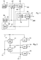
- Figure 1 shows an alternative implementation of the arrangement,
- Figure 2 shows in detail a serial/parallel converter, and
- Figure 3 shows the arrangement in detail.
-
- With reference to Figure 1 the arrangement comprises a
modulator 10, a serial/parallel converter 20, aDA converter 30, adivider 40, aclock generator 50, abus 60, anAD converter 70 and a parallel/serial converter 80. In the implementation shown in the Figure, the serial/parallel converter 20, theDA converter 30 and thedivider 40 are placed into an ASIC circuit 100 (ASIC = Application Specific integrated Circuit). TheAD converter 70 and the parallel/serial converter 80 are in turn placed into anASIC circuit 200. The arrangement can also be implemented for one ASIC circuit. - The
modulator 10 is preferably a sigma-delta modulator, but the modulator can be of another type too. The blocks in theASIC circuit 100 belong to the first structural set of the arrangement, which also comprises the modulator. The blocks in theASIC circuit 200 belong to the second structural set. - Figure 1 shows that an
output signal 11 of the sigma-delta modulator 20 is connected to the input side of the serial/parallel converter 20. The signal generated by the modulator is preferably of PDM type (PDM = Pulse Density Modulation) or of PWM type (=Pulse Width Modulation). Each modulation result of themodulator 10 comprises one or more bits. The modulation result preferably comprises as few bits as possible. In the implementation alternative shown in Figure 1 the modulation result preferably includes one bit. - Figure 1 also shows that the output side of the
converter 20 is connected to the input side of theDA converter 30. In addition, the output side of theAD converter 70 is connected to the input side of the parallel/serial converter 80. Thebus 60 is connected from the output side of theDA converter 30 to the input side of theAD converter 70. The bus, which is analogue, allows the ASIC circuits to be connected with one another. - A
clock generator 50 is connected to the serial/parallel converter 20. Theclock generator 50 generates aclock signal 51, and the pace determined by the clock signal is used to transfer theoutput signal 11 generated by the modulator towards the input side of the serial/parallel converter 20. Thesame clock signal 51 is also conveyed to the parallel/serial converter 80, which generates a serial-mode signal 87. Aclock signal 41 generated by thedivider 40 is also connected to the serial/parallel converter 20 and the serial/parallel converter 80. - Figure 2 shows a serial/parallel converter. Figure 2 illustrates that the serial/
parallel converter 20 is at least partly implemented using flip-flop circuits. The converter can also be implemented using other than flip-flop circuits. The parallel/serial converter 80 can also be implemented, for example, using flip-flop circuits. - The serial/
parallel converter 20 comprises flip-flop circuits circuit 21 and the inputs ofcircuit 23 are connected together. The output ofcircuit 21 is connected to the input ofcircuit 22 and to the input of circuit 24. The output ofcircuit 22 is connected to the input ofcircuit 22. Figure 2 also shows that asignal 41 is connected to thecircuits circuits DA converter 30 as illustrated in Figure 1. - With reference to Figure 2, a
clock signal 51, which may have a frequency of 30 MHz, generated by theclock generator 50 is conveyed as such to the clock inputs ofcircuits circuits divider 40, which divides the frequency of the clock signal that it has received by an integer value. If the converter is three bits in length, said integer value is three. - The
divider 40 generates theclock signal 41 having a frequency that is lower than the frequency of the clock signal being supplied tocircuits circuit - Since
circuits parallel converter 20 forms a delay line, which delays the signals arriving from the modulator. The serial/parallel conversion allows the chance to use the DA converter in the system. The DA converter comprises parallel inputs and parallel outputs. The parallel outputs form abus 60, which is used when the signals formed by theDA converter 20 propagate to theAD converter 70. - With reference to Figure 1 the
bus 60 comprises at least one signal path, in which analogue signal comprising various signal levels is transferred. The type of the analogue signal may be a current signal or a voltage signal. As each signal to be transferred on the signal path is clocked using a clock signal generated by the divider, the clock signal being smaller than the clock frequency used when transferring the output signal of the modulator, then the creation of high frequency noise to the DA-converted signal can be reduced. To be more precise, the created interference remains on the bus at low frequencies, and do not therefore interfere with other apparatuses, for example. The created interference may be for example noise, which is not disturbing, since the interference is of low frequency type. In this case the signal on the signal path of the bus is clocked only using a 10 MHz clock signal. - The method of the invention is applicable to be used both on the DA and AD converter sides. The outputs of the DA and AD converters may be, for example, differential. In addition, at least the AD converter is capable of receiving differential signals too. The arrangement may comprise several parallel DA converters, as well as several parallel AD converters. An AD converted signal can after being converted into serial mode be demodulated, for example, in a sigma delta demodulator.
- In an alternative implementation the arrangement comprises for example two three-bit D/A converters, which are in parallel. If the serial/
parallel converter 20 in the above arrangement receives a two-bit input signal, a six-bit signal is transferred in one go towards the D/A converter. In a situation described above the divider generates a clock signal, which is a sixth of the clock signal that is correspondingly used for clocking a two-bit input signal to the serial/parallel converter 20. In the implementation alternative shown in Figure 1, a one-bit signal arrives at the serial/parallel converter 20, and said signal is converted into a three-bit signal, which is conveyed to the D/A converter for conversion into an analogue signal. - The
AD converter 70 receives the analogue signals arriving from theDA converter 30 and converts them into digital mode. In this case the AD converter simultaneously transmits three of the digital signals it has generated in one go to the parallel/serial converter 80 for conversion. - Figure 3 shows in more detail the
arrangement comprising circuits circuits AD converter 70 and the parallel/serial converter 80. The input of eachcircuit circuits circuits - In the implementation alternative shown in Figure 3, three output signals of the
AD converter 70 are simultaneously clocked in one go to thecircuits circuits clock signal 41 generated by the divider, the clock signal being the same as the one used for clocking thecircuits - A data signal 87 with a data rate equalling the data rate of the
signal 11 is obtained from the output of the parallel/serial converter 80 in the implementation alternative of Figure 3. In signal transmission a clock signal is here used for thecircuits signal 87. Signal is clocked for thecircuits serial converter 80 using the clock signal generated by the divider. The frequency of said clock signal is lower than the clock frequency of the signal used for transferring theoutput signal 87 of the parallel/serial converter 80. - The method comprises two sets of process steps, whereof at least one is performed in the method in order to carry out the method of the invention. A modulated digital output signal in serial mode is generated in the first set of process steps, the output signal being converted into parallel mode. The parallel mode signal is transferred for conversion into analogue mode using a clock signal, whose frequency is lower than the frequency of the clock signal used in serial-mode signal transmission.
- Analogue input signal is received in the second set of process steps, and the input signal is converted into several parallel digital output signals. The generated digital signals are simultaneously transferred for conversion into serial-mode signals using a clock signal, whose frequency is lower than the frequency of the clock signal used in serial-mode signal transmission.
- Even though the invention has been described above with reference to the example of the accompanying drawings, it is obvious that the invention is not restricted thereto but can be modified in various ways within the scope of the inventive idea disclosed in the attached claims.
Claims (12)
- A method for reducing interference created in an output signal in connection with signal conversion, characterized in that in order to carry out the method two sets of process steps can be employed, whereof at least one is performed in this method,the first set of process steps comprises the step ofgenerating a digital modulated input signal in serial mode which is converted into parallel mode, and simultaneously several digital signals are transferred using a clock signal for conversion into analogue output signals, the frequency of the clock signal being lower than the frequency of the clock signal used in serial-mode signal transmission,the second set of process steps comprises the step ofreceiving analogue input signal, which is converted into several parallel digital output signals which are simultaneously transferred using a clock signal for conversion into serial mode signals, the frequency of the clock signal being lower than the frequency of the clock signal used in serial-mode signal transmission.
- A method as claimed in claim 1, characterized in that said modulated signal is generated using sigma-delta modulation.
- A method as claimed in claim 1, characterized in that the input signal is delayed when converting the digital input signal into parallel mode.
- A method as claimed in claim 1, characterized in that each generated analogue signal is transferred to the bus, where each signal is transferred using a clock signal having a frequency that equals the one in the clock signal which is used for clocking signals for conversion into parallel mode.
- A method as claimed in claim 1, characterized in that the digital input signal is converted into an analogue output voltage.
- A method as claimed in claim 1, characterized in that the digital input signal is converted into an analogue output current.
- An arrangement for reducing interference created in an output signal in connection with signal conversion, characterized in that the arrangement may employ two structural sets, whereof the arrangement comprises at least one,the first structural set comprises a modulator (10) arranged to modulate the signal, and a DA converter (30) arranged to convert the serial-mode input signal arriving from the modulator into an analogue output signal, anda serial/parallel converter (20) arranged to convert the modulated signal into parallel mode, anda divider (40) for generating a clock signal, the frequency of the clock signal generated by the divider being lower than the frequency of the clock signal used in serial-mode input signal transmission, and the divider (40) is arranged to simultaneously clock several signals to the DA converter (30), andthe second structural set comprises an AD converter (70) arranged to convert an analogue input signal into several parallel digital output signals, anda parallel/serial converter (80) arranged to receive several simultaneously arriving digital signals for conversion into serial mode signals using a clock signal, the frequency of which being lower than the frequency of the clock signal used in serial-mode signal transmission.
- An arrangement as claimed in claim 7, characterized in that the modulator is a sigma-delta modulator.
- An arrangement as claimed in claim 7, characterized in that the serial/parallel converter (20) is arranged to delay the digital input signal.
- An arrangement as claimed in claim 7, characterized in that the arrangement comprises a parallel bus (60) between the DA and AD converters, the divider (40) being arranged to transfer the output signals in the parallel bus using a clock signal, whose frequency equals the frequency of the clock signal that clocks the signals to the DA converter and from the AD converter.
- An arrangement as claimed in claim 7, characterized in that the DA converter (30) is arranged to convert the digital input signal to an analogue output voltage.
- An arrangement as claimed in claim 7, characterized in that the DA converter (30) is arranged to convert the digital input signal to an analogue output current.
Applications Claiming Priority (2)
| Application Number | Priority Date | Filing Date | Title |
|---|---|---|---|
| FI20001913A FI20001913A7 (en) | 2000-08-30 | 2000-08-30 | Method and arrangement for reducing interference |
| FI20001913 | 2000-08-30 |
Publications (1)
| Publication Number | Publication Date |
|---|---|
| EP1195905A1 true EP1195905A1 (en) | 2002-04-10 |
Family
ID=8558986
Family Applications (1)
| Application Number | Title | Priority Date | Filing Date |
|---|---|---|---|
| EP01000368A Withdrawn EP1195905A1 (en) | 2000-08-30 | 2001-08-15 | D/A-A/D method and arrangement for reducing interference |
Country Status (3)
| Country | Link |
|---|---|
| US (1) | US6567020B2 (en) |
| EP (1) | EP1195905A1 (en) |
| FI (1) | FI20001913A7 (en) |
Families Citing this family (2)
| Publication number | Priority date | Publication date | Assignee | Title |
|---|---|---|---|---|
| US8527908B2 (en) * | 2008-09-26 | 2013-09-03 | Apple Inc. | Computer user interface system and methods |
| JPWO2010131428A1 (en) * | 2009-05-14 | 2012-11-01 | パナソニック株式会社 | communication cable |
Citations (5)
| Publication number | Priority date | Publication date | Assignee | Title |
|---|---|---|---|---|
| EP0092083A2 (en) * | 1982-04-17 | 1983-10-26 | Neumann Elektronik GmbH | Electronic message sender for transmitting and/or recording messages on a telephone line |
| US4670792A (en) * | 1981-05-08 | 1987-06-02 | Agence France Presse | Method and device for recreation of an analog luminance signal from a digital signal |
| JPH0685762A (en) * | 1992-09-01 | 1994-03-25 | Fujitsu Ltd | Data communication system with a/d-d/a-conversion protection function |
| JPH07123368A (en) * | 1993-10-20 | 1995-05-12 | Fujitsu General Ltd | Scan converter |
| JPH07212229A (en) * | 1994-01-21 | 1995-08-11 | Matsushita Electric Ind Co Ltd | A / D / D / A converter |
Family Cites Families (11)
| Publication number | Priority date | Publication date | Assignee | Title |
|---|---|---|---|---|
| CA1278347C (en) | 1987-09-22 | 1990-12-27 | Shoichi Mizoguchi | Correlation detecting circuit operable in a low frequency |
| JP2970907B2 (en) * | 1988-04-13 | 1999-11-02 | 株式会社ナムコ | Analog signal synthesizer in PCM |
| JPH02156732A (en) | 1988-12-09 | 1990-06-15 | Hitachi Ltd | demodulator |
| EP0660555A3 (en) | 1989-01-09 | 1995-09-13 | Fujitsu Ltd | Device for multiplexing and demultiplexing digital signals. |
| KR930002134B1 (en) * | 1990-10-24 | 1993-03-26 | 삼성전자 주식회사 | Parallel data transfer processing circuit |
| US5541665A (en) * | 1993-12-22 | 1996-07-30 | Hitachi, Ltd. | Image processing apparatus with change over of clock signals |
| US6202108B1 (en) * | 1997-03-13 | 2001-03-13 | Bull S.A. | Process and system for initializing a serial link between two integrated circuits comprising a parallel-serial port using two clocks with different frequencies |
| US6282236B1 (en) * | 1997-04-03 | 2001-08-28 | Lucent Technologies, Inc. | Modem designs, and systems using the modem designs for communicating information between a number of remote locations and one or more central locations |
| US6031473A (en) * | 1997-11-17 | 2000-02-29 | Advanced Micro Devices, Inc. | Digital communications using serialized delay line |
| US6160859A (en) * | 1998-10-19 | 2000-12-12 | Motorola, Inc. | Integrated multi-mode bandpass sigma-delta receiver subsystem with interference mitigation and method of using the same |
| KR20010074694A (en) | 1999-05-12 | 2001-08-09 | 요트.게.아. 롤페즈 | Apparatus for decoding a serial datastream of channel words into a datastream of information words |
-
2000
- 2000-08-30 FI FI20001913A patent/FI20001913A7/en unknown
-
2001
- 2001-08-15 EP EP01000368A patent/EP1195905A1/en not_active Withdrawn
- 2001-08-28 US US09/941,320 patent/US6567020B2/en not_active Expired - Lifetime
Patent Citations (5)
| Publication number | Priority date | Publication date | Assignee | Title |
|---|---|---|---|---|
| US4670792A (en) * | 1981-05-08 | 1987-06-02 | Agence France Presse | Method and device for recreation of an analog luminance signal from a digital signal |
| EP0092083A2 (en) * | 1982-04-17 | 1983-10-26 | Neumann Elektronik GmbH | Electronic message sender for transmitting and/or recording messages on a telephone line |
| JPH0685762A (en) * | 1992-09-01 | 1994-03-25 | Fujitsu Ltd | Data communication system with a/d-d/a-conversion protection function |
| JPH07123368A (en) * | 1993-10-20 | 1995-05-12 | Fujitsu General Ltd | Scan converter |
| JPH07212229A (en) * | 1994-01-21 | 1995-08-11 | Matsushita Electric Ind Co Ltd | A / D / D / A converter |
Non-Patent Citations (3)
| Title |
|---|
| PATENT ABSTRACTS OF JAPAN vol. 018, no. 342 (E - 1570) 28 June 1994 (1994-06-28) * |
| PATENT ABSTRACTS OF JAPAN vol. 1995, no. 08 29 September 1995 (1995-09-29) * |
| PATENT ABSTRACTS OF JAPAN vol. 1995, no. 11 26 December 1995 (1995-12-26) * |
Also Published As
| Publication number | Publication date |
|---|---|
| US6567020B2 (en) | 2003-05-20 |
| FI20001913A7 (en) | 2002-03-01 |
| FI20001913A0 (en) | 2000-08-30 |
| US20020064243A1 (en) | 2002-05-30 |
Similar Documents
| Publication | Publication Date | Title |
|---|---|---|
| US7599447B2 (en) | Method and system for a reduced emissions direct drive transmitter for unshielded twisted pair (UTP) applications | |
| US6031473A (en) | Digital communications using serialized delay line | |
| US5610606A (en) | 1-bit D/A conversion circuit | |
| US7103110B2 (en) | Dual phase pulse modulation encoder circuit | |
| EP0717496A1 (en) | High speed parallel/serial interface | |
| US6567020B2 (en) | Method and arrangement for reducing interference | |
| US4686676A (en) | Apparatus and method for determining true data in a digital data stream from distorted data | |
| US6466143B2 (en) | Non-return-to-zero DAC using reference sine wave signals | |
| US7283011B2 (en) | Method for performing dual phase pulse modulation | |
| US7391716B2 (en) | Semiconductor integrated circuit and data transmission system | |
| US6738002B2 (en) | SD-ADC with digital dither signal processing | |
| US20050057319A1 (en) | Pulse modulation | |
| JP2004514325A (en) | System and method for transmitting and receiving data signals over a clock signal line | |
| US7489915B2 (en) | Squelch circuit and communication apparatus used with the same | |
| US6532441B1 (en) | Parallel oversampled decimator filter | |
| US6756926B2 (en) | Optical transmitter and code conversion circuit used therefor | |
| JP3035817B2 (en) | Clock recovery device | |
| EP1041789A3 (en) | OFDM modulator synchronized to external device | |
| EP0305467B1 (en) | Method and apparatus for transmitting a synchronous data signal on a transmission medium on which the transmission rate is greater than the data signal bit rate | |
| JPH11340839A (en) | Parallel signal serial transmission device | |
| JP3487228B2 (en) | Manchester encoder | |
| CN100589464C (en) | Bi-phase pulse modulation encoder circuit | |
| JP2591286B2 (en) | DA converter | |
| JPH04160821A (en) | Pulse width modulator | |
| KR100210394B1 (en) | Multi-value Logical Data Transmission System |
Legal Events
| Date | Code | Title | Description |
|---|---|---|---|
| PUAI | Public reference made under article 153(3) epc to a published international application that has entered the european phase |
Free format text: ORIGINAL CODE: 0009012 |
|
| AK | Designated contracting states |
Kind code of ref document: A1 Designated state(s): DE FR GB IT Kind code of ref document: A1 Designated state(s): AT BE CH CY DE DK ES FI FR GB GR IE IT LI LU MC NL PT SE TR |
|
| AX | Request for extension of the european patent |
Free format text: AL;LT;LV;MK;RO;SI |
|
| 17P | Request for examination filed |
Effective date: 20020801 |
|
| 17Q | First examination report despatched |
Effective date: 20021031 |
|
| AKX | Designation fees paid |
Free format text: DE FR GB IT |
|
| GRAH | Despatch of communication of intention to grant a patent |
Free format text: ORIGINAL CODE: EPIDOS IGRA |
|
| STAA | Information on the status of an ep patent application or granted ep patent |
Free format text: STATUS: THE APPLICATION IS DEEMED TO BE WITHDRAWN |
|
| 18D | Application deemed to be withdrawn |
Effective date: 20030905 |