EP1195255A1 - Thermal print head and method of manufacture thereof - Google Patents
Thermal print head and method of manufacture thereof Download PDFInfo
- Publication number
- EP1195255A1 EP1195255A1 EP00937270A EP00937270A EP1195255A1 EP 1195255 A1 EP1195255 A1 EP 1195255A1 EP 00937270 A EP00937270 A EP 00937270A EP 00937270 A EP00937270 A EP 00937270A EP 1195255 A1 EP1195255 A1 EP 1195255A1
- Authority
- EP
- European Patent Office
- Prior art keywords
- outermost layer
- electrode pattern
- sic
- thermal printhead
- layer
- Prior art date
- Legal status (The legal status is an assumption and is not a legal conclusion. Google has not performed a legal analysis and makes no representation as to the accuracy of the status listed.)
- Withdrawn
Links
Images


Classifications
-
- B—PERFORMING OPERATIONS; TRANSPORTING
- B41—PRINTING; LINING MACHINES; TYPEWRITERS; STAMPS
- B41J—TYPEWRITERS; SELECTIVE PRINTING MECHANISMS, i.e. MECHANISMS PRINTING OTHERWISE THAN FROM A FORME; CORRECTION OF TYPOGRAPHICAL ERRORS
- B41J2/00—Typewriters or selective printing mechanisms characterised by the printing or marking process for which they are designed
- B41J2/315—Typewriters or selective printing mechanisms characterised by the printing or marking process for which they are designed characterised by selective application of heat to a heat sensitive printing or impression-transfer material
- B41J2/32—Typewriters or selective printing mechanisms characterised by the printing or marking process for which they are designed characterised by selective application of heat to a heat sensitive printing or impression-transfer material using thermal heads
- B41J2/335—Structure of thermal heads
-
- B—PERFORMING OPERATIONS; TRANSPORTING
- B41—PRINTING; LINING MACHINES; TYPEWRITERS; STAMPS
- B41J—TYPEWRITERS; SELECTIVE PRINTING MECHANISMS, i.e. MECHANISMS PRINTING OTHERWISE THAN FROM A FORME; CORRECTION OF TYPOGRAPHICAL ERRORS
- B41J2/00—Typewriters or selective printing mechanisms characterised by the printing or marking process for which they are designed
- B41J2/315—Typewriters or selective printing mechanisms characterised by the printing or marking process for which they are designed characterised by selective application of heat to a heat sensitive printing or impression-transfer material
- B41J2/32—Typewriters or selective printing mechanisms characterised by the printing or marking process for which they are designed characterised by selective application of heat to a heat sensitive printing or impression-transfer material using thermal heads
- B41J2/335—Structure of thermal heads
- B41J2/33505—Constructional details
- B41J2/33525—Passivation layers
-
- B—PERFORMING OPERATIONS; TRANSPORTING
- B41—PRINTING; LINING MACHINES; TYPEWRITERS; STAMPS
- B41J—TYPEWRITERS; SELECTIVE PRINTING MECHANISMS, i.e. MECHANISMS PRINTING OTHERWISE THAN FROM A FORME; CORRECTION OF TYPOGRAPHICAL ERRORS
- B41J2/00—Typewriters or selective printing mechanisms characterised by the printing or marking process for which they are designed
- B41J2/315—Typewriters or selective printing mechanisms characterised by the printing or marking process for which they are designed characterised by selective application of heat to a heat sensitive printing or impression-transfer material
- B41J2/32—Typewriters or selective printing mechanisms characterised by the printing or marking process for which they are designed characterised by selective application of heat to a heat sensitive printing or impression-transfer material using thermal heads
- B41J2/335—Structure of thermal heads
- B41J2/33505—Constructional details
- B41J2/3353—Protective layers
-
- B—PERFORMING OPERATIONS; TRANSPORTING
- B41—PRINTING; LINING MACHINES; TYPEWRITERS; STAMPS
- B41J—TYPEWRITERS; SELECTIVE PRINTING MECHANISMS, i.e. MECHANISMS PRINTING OTHERWISE THAN FROM A FORME; CORRECTION OF TYPOGRAPHICAL ERRORS
- B41J2/00—Typewriters or selective printing mechanisms characterised by the printing or marking process for which they are designed
- B41J2/315—Typewriters or selective printing mechanisms characterised by the printing or marking process for which they are designed characterised by selective application of heat to a heat sensitive printing or impression-transfer material
- B41J2/32—Typewriters or selective printing mechanisms characterised by the printing or marking process for which they are designed characterised by selective application of heat to a heat sensitive printing or impression-transfer material using thermal heads
- B41J2/335—Structure of thermal heads
- B41J2/3355—Structure of thermal heads characterised by materials
-
- B—PERFORMING OPERATIONS; TRANSPORTING
- B41—PRINTING; LINING MACHINES; TYPEWRITERS; STAMPS
- B41J—TYPEWRITERS; SELECTIVE PRINTING MECHANISMS, i.e. MECHANISMS PRINTING OTHERWISE THAN FROM A FORME; CORRECTION OF TYPOGRAPHICAL ERRORS
- B41J2/00—Typewriters or selective printing mechanisms characterised by the printing or marking process for which they are designed
- B41J2/315—Typewriters or selective printing mechanisms characterised by the printing or marking process for which they are designed characterised by selective application of heat to a heat sensitive printing or impression-transfer material
- B41J2/32—Typewriters or selective printing mechanisms characterised by the printing or marking process for which they are designed characterised by selective application of heat to a heat sensitive printing or impression-transfer material using thermal heads
- B41J2/335—Structure of thermal heads
- B41J2/33555—Structure of thermal heads characterised by type
- B41J2/3357—Surface type resistors
-
- B—PERFORMING OPERATIONS; TRANSPORTING
- B41—PRINTING; LINING MACHINES; TYPEWRITERS; STAMPS
- B41J—TYPEWRITERS; SELECTIVE PRINTING MECHANISMS, i.e. MECHANISMS PRINTING OTHERWISE THAN FROM A FORME; CORRECTION OF TYPOGRAPHICAL ERRORS
- B41J2/00—Typewriters or selective printing mechanisms characterised by the printing or marking process for which they are designed
- B41J2/315—Typewriters or selective printing mechanisms characterised by the printing or marking process for which they are designed characterised by selective application of heat to a heat sensitive printing or impression-transfer material
- B41J2/32—Typewriters or selective printing mechanisms characterised by the printing or marking process for which they are designed characterised by selective application of heat to a heat sensitive printing or impression-transfer material using thermal heads
- B41J2/335—Structure of thermal heads
- B41J2/3359—Manufacturing processes
Definitions
- the present invention relates to a thermal printhead and a method of making the same.
- a common thermal printhead currently in use includes a substrate formed with an electrode pattern including a common electrode and individual electrodes.
- the substrate is also formed with a heating resister connected to the electrode pattern. Further, the electrode pattern and the heating resister are covered and protected by a multi-layer protective coating.
- an outermost layer of the protective coating makes direct contact with the printing paper, and therefore worn out after repeated contacts with the paper.
- an inner layer is gradually worn by friction, eventually exposing the heating resister and the electrodes.
- a problem of e.g. white or black streaks found in the print leads to a problem of e.g. white or black streaks found in the print.
- the protective coating can be made more durable if the outermost layer is made significantly thicker. However, this causes another problem that an increased distance from the heating resister to the paper reduces thermal response, resulting in poor printing quality.
- non-oxide ceramics superior in a number of coating characteristics are employed as a material for the outermost layer.
- silicon carbide (SiC) and silicon nitride (Si 3 N 4 ) are used extensively. These ceramic materials in general have a high hardness and are believed to have a superior anti-wear characteristic. For this reason, it is believed that use of these materials should allow the outermost layer to be made as accordingly thin as 4 ⁇ m for increased thermal response.
- the friction coefficient is a factor that determines the anti-wear characteristic and slidability, and that it is impossible to improve the anti-wear characteristic and slidability if the friction coefficient is high in general. Because of this, even if the outermost layer of the protective coating is made of such a material as SiC and Si 3 N 4 , the anti-wear characteristic and slidability cannot be improved significantly, and there is still room for research and development in the improvement of these.
- the outermost layer there is another problem related to adhesion between the outermost layer and the primer layer. Specifically, if the outermost layer is formed of a common oxide ceramic, a good adhesion with the primer layer is not obtained. If the outermost layer is formed of a hard non-oxide material such as SiC and Si 3 N 4 , there is another problem that once a scratch is formed due to an external force, the coating can easily come off along the scratch because of the high hardness.
- Another object of the present invention is to provide a method of manufacturing such a thermal printhead.
- a thermal printhead comprising: a substrate; an electrode pattern formed on the substrate, including a common electrode and a plurality of individual electrodes; a plurality of heating dots connected to the electrode pattern; and a protective coating including a plurality of layers covering the electrode pattern and the heating dots.
- the protective coating includes an outermost layer composed mainly of SiC and an admixture of carbon.
- the carbon content in the outermost layer is not lower than 60 mol percent.
- the protective coating includes, in addition to the outermost layer, a thick glass layer covering the heating dots and the electrode pattern, a thin glass layer formed on the thick glass layer, and an adhesion layer formed between the thin glass layer and the outermost layer.
- the heating dots are provided by a straight thick-film resister.
- the outermost layer contains, in addition to SiC, carbon as the admixture.
- a method of manufacturing a thermal printhead comprising: a substrate; an electrode pattern formed on the substrate, including a common electrode and a plurality of individual electrodes; a plurality of heating dots connected to the electrode pattern; and a protective coating including a plurality of layers covering the electrode pattern and the heating dots.
- the outermost layer of the protective coating is formed by spattering with a use of a target composed mainly of SiC and an admixture of carbon.
- the carbon content in the target is 60-80 mol percent.
- film characteristic of the resulting outermost layer can be controlled.
- the spattering is provided by a reactive spattering.
- the outermost layer is composed mainly of SiC but also include carbon as an admixture.
- a carbon mol percentage with respect to all of the composing atoms is slightly higher than in the equilibrium of pure SiC, which results in a various change in film characteristics of the outermost layer.
- the outermost layer including an admixture of carbon has a lower film stress than the layer provided by pure SiC, providing a denser layer .
- the outmost layer of the above arrangement has a low electric conductivity, which is not charged by the sliding friction with the paper. On the other hand, the lower conductivity causes very little electric corrosion.
- the carbon content in the outermost layer can be adjusted by means of a reactive spattering, in which capture of carbon into the outermost layer is controlled at an atomic level. Through this control, material composition when forming the outermost layer can be optimized.
- Fig. 1 and Fig. 2 show a thick-film thermal printhead 1 according to a preferred embodiment of the present invention.
- the thermal printhead 1 comprises a ceramic substrate 2 having an upper surface formed with a heat accumulating glaze layer 6, and an electrode pattern 3 formed on an upper surface of the glaze layer 6.
- the electrode pattern 3 includes a common electrode 30 and a plurality of individual electrodes 31.
- the common electrode 30 includes a plurality of comb-teeth like extensions 30a, and each of the extensions 30a is formed between two mutually adjacent individual electrodes 31.
- each of the individual electrodes 31 has an end 31a formed between two mutually adjacent extensions 30a of the common electrode 30.
- Each individual electrode 31 has another end 31b, which serves as a connecting pad.
- the connecting pad 31b is connected via a wire to a corresponding but unillustrated drive IC.
- the electrode pattern 3 is formed by first printing and baking a pattern of resinated gold, and then etching the pattern by means of photolithography.
- the extensions 30a of the common electrode 30, and the individual electrodes 31 are crossed by a thick-film heating resister 5 that extends straightly.
- a portion sandwiched by mutually adjacent two extensions 30a (a cross-hatched portion in Fig. 1) serves as a unit of heating dot 50.
- the heating dot 50 is heated by a current from a corresponding but unillustrated drive IC.
- the heating resister 5 is formed, for example, by printing and baking a resister paste including ruthenium oxide.
- the thermal printhead 1 is provided, as shown in Fig. 2, with a protective coating 8 that covers the electrode pattern 3 and the heating resister 5.
- the protective coating 8 has a multi-layer structure including four layers, namely a thick glass layer 81, a thin glass layer 82, a primer layer 83 serving as an adhesive layer, and an outermost layer 84 which makes contact directly with the printing paper.
- the thick glass layer 81 is formed by printing and baking a glass paste, as an amorphous-glass thick film having e.g. a thickness of about 10 ⁇ m and a Vickers hardness of 500-600 kg/m 2 .
- the glass paste used for the formation of this thick film glass layer 81 contains for example about 26.5 weight percent of a resin component and about 73.5 weight percent of glass component.
- the thin glass layer 82 is formed by a suitable method such as spattering, CVD method and vapor deposition, as a thin film of silicon dioxide (SiO 2 ) having a thickness of about 0.6 ⁇ m and a Vickers hardness of 500 - 700 kg/m 2 .
- the primer layer 83 is formed by a suitable method such as spattering, CVD method and vapor deposition, as a thin film of silicon carbide (SiC) having a thickness of about 2.0 ⁇ m and a Vickers hardness of 1600-1800 kg/m 2 .
- the primer layer 83 may be formed of a metal such as titanium and tungsten, or titanium carbide.
- the outermost layer 84 is formed by e.g. spattering to a thickness of about 4 ⁇ m and a Vickers hardness of about 1200 kg/m 2 , from a film formation material.
- the film formation material is a ceramic material containing silicon carbide (SiC) as a main component, and carbon (C) as an admixture element (hereinafter will simply be written as "C-SiC".) More specifically, C-SiC that provides the outer most layer 84 has its carbon (C) content adjusted to 60-80 mol percent.
- C-SiC containing carbon (C) as an additional element
- SiC pure silicon carbide
- the outermost layer 84 formed of the C-SiC having the composition described above is formed by means of a reactive spattering, using a C-SiC target having the same composition.
- a desired film characteristic can be obtained by varying spattering conditions such as using a target of a different composition, and varying a concentration of active gases such as hydrogen and methane in an atmosphere.
- Fig. 3 is a graph showing how a friction coefficient measurement changed in a wearing test conducted to a C-SiC film (the outermost layer 84), as a comparison with a conventional film.
- the wearing test was made on a commercially available friction wear tester (manufactured by Shinko Engineering Co., Ltd.) under the following test conditions. Temperature 24°C Ball Carbon Steel Ball Load 500 g Stroke 6 mm Frequency 2 Hz
- the test conditions will be described briefly. Under a temperature condition of 24°C, the ball was pressed by a force of 500g to a specimen (film) and moved to wear out the specimen. In the test, the stroke of the ball (a one-way distance covered in a forward and a rearward movement) was 6 mm (that is, a total ball travel per reciprocation cycle was 12 mm). Frequency (the number of cycles per second) was 2 Hz. The specimen was rubbed to be worn in a total of 1500 cycles.
- the C-SiC film used as the outermost layer 84 according to the present embodiment showed a sharp decrease in its friction coefficient at about 200 rubbing cycles, and then kept an extremely low value, i.e. 0.05, permanently. Further, eventually, an amount of wear in the C-Sic film was less than half (or 0.4 ⁇ m) as in the conventional SiC film and Si 3 N 4 film. This is probably because the addition of carbon (C) to silicon carbide has made the film surface that serves as the sliding surface into a dense structure which is extremely resistant to oxidization into silicon oxide (SiO 2 ).
- the C-Sic film according to the present embodiment has a friction coefficient that is extremely lower than the conventional films of different composition, and therefore the amount of wear is reduced. As a result, sufficient improvement is achieved in the slidability and anti-wear characteristic according to the C-Sic film.
- the C-SiC film has a tensile strength which is greater than twice the strength of e.g. the conventional Si 3 N 4 film. Therefore, use of the C-SiC film as the outermost layer 84 enables to improve adhesion with the primer layer 83, and to improve protection against external force in that the layer becomes less prone to damages such as a scratch as well as less prone to the problem of coming off the under layer.
- the C-SiC film by adjusting the carbon (C) mol percentage to a value not greater than 80 (and on the other hand, by adjusting the silicon (Si) mol percentage to a value not smaller than 20), it becomes possible to increase the film's specific resistance to not smaller than about 10 6 ohm/cm. With this condition, since the film itself has an extremely low conductivity, it becomes possible to prevent the problem of electric corrosion such as that water on the film surface causes ionizing and elusion. On the other hand, since the C-SiC film has a slight conductivity, the outermost layer 84 provided by this film, being in contact with e.g. the common electrode 30, can discharge static electricity generated by the friction with the paper, making possible to prevent the problem of electrostatic puncture.
- the protective coating 3 as a whole can be made thin, which enables to continue with a high thermal response from the heating resister 5 to the paper, and therefore to maintain a high printing quality. Further, since the C-SiC film is ceramic, it has no problem in terms of heat resistance.
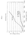
- Fig. 4 is a graph showing a result of a performance test of the thermal printhead according to the present embodiment which has the outermost layer formed of the C-SiC film (containing 80 mol percent of carbon component and 20 mol percent of Silicon component). The result is compared with a conventional head having the outermost layer formed of the SiC film.
- the performance test was performed at 100 percent duty (i.e. all of the heating dots were driven to make continuous solid black printing), with the paper slid on the outermost layer. Evaluation of the test was made by an amount of wear of the outermost layer at predetermined points of printing distance.
- the thermal printhead according to the present embodiment is suitable for a printing apparatus which requires a significantly high durability (for example, a barcode printer).
- the present invention is also applicable to a thin-film thermal printhead.
Landscapes
- Engineering & Computer Science (AREA)
- Manufacturing & Machinery (AREA)
- Electronic Switches (AREA)
Abstract
A thermal printhead (1) comprises a substrate (2), an
electrode pattern (3) formed on the substrate, including a
common electrode and a plurality of individual electrodes,
a heating resister (5) connected to the electrode pattern (3),
and a protective coating (8) including a plurality of layers
(81, 82, 83, 84) covering the electrode pattern (3) and the
heating resister (5). The protective coating includes an
outermost layer (84) composed mainly of SiC and an admixture
of carbon.
Description
The present invention relates to a thermal printhead and
a method of making the same.
A common thermal printhead currently in use includes a
substrate formed with an electrode pattern including a common
electrode and individual electrodes. The substrate is also
formed with a heating resister connected to the electrode
pattern. Further, the electrode pattern and the heating
resister are covered and protected by a multi-layer
protective coating.
In use, an outermost layer of the protective coating makes
direct contact with the printing paper, and therefore worn
out after repeated contacts with the paper. For example, when
the printing is continued for a distance of over 100
kilometers, not only the outermost layer but also an inner
layer is gradually worn by friction, eventually exposing the
heating resister and the electrodes. Such a situation leads
to a problem of e.g. white or black streaks found in the print.
The protective coating can be made more durable if the
outermost layer is made significantly thicker. However,
this causes another problem that an increased distance from
the heating resister to the paper reduces thermal response,
resulting in poor printing quality.
In order to avoid such a problem, a variety of non-oxide
ceramics superior in a number of coating characteristics are
employed as a material for the outermost layer. Among them,
silicon carbide (SiC) and silicon nitride (Si3N4) are used
extensively. These ceramic materials in general have a high
hardness and are believed to have a superior anti-wear
characteristic. For this reason, it is believed that use of
these materials should allow the outermost layer to be made
as accordingly thin as 4µm for increased thermal response.
However, even if such a hard material as SiC of Si3N4 is
used for the outermost layer, it is still impossible to
improve all film characteristics required of the outermost
layer. Recently in particular, a demonstrating test has
proven that even such hard materials did not provide as
improved anti-wear characteristic as expected. For example,
in a wearing test conducted to SiC, a thin coating of SiC was
worn by repeated rubbing with a metal ball under a
predetermined condition (to be detailed later). Result was,
as shown in Fig. 3, that after about 1000 times of rubbing
cycle, a gradual increase was found in friction coefficient,
which eventually resulted in an amount of wear as much as 1.1
m. This is due to a chemical reaction at an atom-molecular
level on the coating surface, in which the surface formed as
SiC changed to silicon dioxide (SiO2). As for Si3N4, as will
be clear from Fig. 3, its friction coefficient was found to
be fairly high even at the beginning.
As described above, it is clear from the graph in Fig.
3 that the friction coefficient is a factor that determines
the anti-wear characteristic and slidability, and that it is
impossible to improve the anti-wear characteristic and
slidability if the friction coefficient is high in general.
Because of this, even if the outermost layer of the protective
coating is made of such a material as SiC and Si3N4, the
anti-wear characteristic and slidability cannot be improved
significantly, and there is still room for research and
development in the improvement of these.
On the other hand, there is another problem related to
adhesion between the outermost layer and the primer layer.
Specifically, if the outermost layer is formed of a common
oxide ceramic, a good adhesion with the primer layer is not
obtained. If the outermost layer is formed of a hard
non-oxide material such as SiC and Si3N4, there is another
problem that once a scratch is formed due to an external force,
the coating can easily come off along the scratch because of
the high hardness.
Still another problem exists in the field of
electrostatic puncture. Specifically, since the oxide
ceramics, SiC and Si3N4 have very low electronic conductivity,
when they are slid on the printing paper, friction can cause
the outermost layer to be electrically charged, which may lead
to the electrostatic puncture. In order to prevent this, an
electrically conducting material can be added. This has
solved the problem of electrostatic puncture, but it has posed
still another problem of electric corrosion that water
condensation for example on the head surface causes
ionization and elusion.
It is therefore an object of the present invention to
provide a thermal printhead having a good slidability with
respect particularly to the printing paper and an improved
anti-wear characteristic, by changing material composition
of the outermost layer.
Another object of the present invention is to provide a
method of manufacturing such a thermal printhead.
According to a first aspect of the present invention,
there is provided a thermal printhead comprising: a
substrate; an electrode pattern formed on the substrate,
including a common electrode and a plurality of individual
electrodes; a plurality of heating dots connected to the
electrode pattern; and a protective coating including a
plurality of layers covering the electrode pattern and the
heating dots. With the above, the protective coating
includes an outermost layer composed mainly of SiC and an
admixture of carbon.
Preferably, the carbon content in the outermost layer is
not lower than 60 mol percent.
According to a preferred embodiment of the present
invention, the protective coating includes, in addition to
the outermost layer, a thick glass layer covering the heating
dots and the electrode pattern, a thin glass layer formed on
the thick glass layer, and an adhesion layer formed between
the thin glass layer and the outermost layer. Further, the
heating dots are provided by a straight thick-film resister.
According to the thermal printhead having the above
construction and the arrangement, the outermost layer
contains, in addition to SiC, carbon as the admixture. As
a result, slidability (anti-wear characteristic) and
adhesion to the primer layer can be improved by varying an
amount of carbon inclusion.
According to a second aspect of the present invention,
there is provided a method of manufacturing a thermal
printhead comprising: a substrate; an electrode pattern
formed on the substrate, including a common electrode and a
plurality of individual electrodes; a plurality of heating
dots connected to the electrode pattern; and a protective
coating including a plurality of layers covering the
electrode pattern and the heating dots. In this method, the
outermost layer of the protective coating is formed by
spattering with a use of a target composed mainly of SiC and
an admixture of carbon.
Preferably, the carbon content in the target is 60-80 mol
percent. By adjusting the carbon content within this range,
film characteristic of the resulting outermost layer can be
controlled.
According to a preferred embodiment of the present
invention, the spattering is provided by a reactive
spattering.
According to the above method of manufacture, the
outermost layer is composed mainly of SiC but also include
carbon as an admixture. In the outermost layer thus formed,
a carbon mol percentage with respect to all of the composing
atoms is slightly higher than in the equilibrium of pure SiC,
which results in a various change in film characteristics of
the outermost layer. Specifically, in the outermost layer
composed of a mixture of pure SiC and extra carbon, even if
the rubbing by the printing paper continues for a long
distance, an extremely low friction coefficient is maintained
for a long time. Further, the outermost layer including an
admixture of carbon has a lower film stress than the layer
provided by pure SiC, providing a denser layer . This improves
adhesion to the primer layer and hardness, resulting in
improvement in mechanical strength. Further, the outmost
layer of the above arrangement has a low electric conductivity,
which is not charged by the sliding friction with the paper.
On the other hand, the lower conductivity causes very little
electric corrosion.
The functions and advantages described above is most
significant when the carbon content in the outermost layer
is from 60-80 mol percent.
The carbon content in the outermost layer can be adjusted
by means of a reactive spattering, in which capture of carbon
into the outermost layer is controlled at an atomic level.
Through this control, material composition when forming the
outermost layer can be optimized.
Other characteristics and advantages of the present
invention will become clearer from the following description
to be presented with reference to the accompanying drawings.
Hereinafter, a preferred embodiment of the present
invention will be described specifically, with reference to
the attached drawings.
Fig. 1 and Fig. 2 show a thick-film thermal printhead 1
according to a preferred embodiment of the present invention.
The thermal printhead 1 comprises a ceramic substrate 2 having
an upper surface formed with a heat accumulating glaze layer
6, and an electrode pattern 3 formed on an upper surface of
the glaze layer 6. The electrode pattern 3 includes a common
electrode 30 and a plurality of individual electrodes 31. The
common electrode 30 includes a plurality of comb-teeth like
extensions 30a, and each of the extensions 30a is formed
between two mutually adjacent individual electrodes 31.
Likewise, each of the individual electrodes 31 has an end 31a
formed between two mutually adjacent extensions 30a of the
common electrode 30. Each individual electrode 31 has
another end 31b, which serves as a connecting pad. The
connecting pad 31b is connected via a wire to a corresponding
but unillustrated drive IC. The electrode pattern 3 is formed
by first printing and baking a pattern of resinated gold, and
then etching the pattern by means of photolithography.
The extensions 30a of the common electrode 30, and the
individual electrodes 31 are crossed by a thick-film heating
resister 5 that extends straightly. In this heating resister
5, a portion sandwiched by mutually adjacent two extensions
30a (a cross-hatched portion in Fig. 1) serves as a unit of
heating dot 50. The heating dot 50 is heated by a current
from a corresponding but unillustrated drive IC. The heating
resister 5 is formed, for example, by printing and baking a
resister paste including ruthenium oxide.
Further, the thermal printhead 1 is provided, as shown
in Fig. 2, with a protective coating 8 that covers the
electrode pattern 3 and the heating resister 5. The
protective coating 8 has a multi-layer structure including
four layers, namely a thick glass layer 81, a thin glass layer
82, a primer layer 83 serving as an adhesive layer, and an
outermost layer 84 which makes contact directly with the
printing paper.
The thick glass layer 81 is formed by printing and baking
a glass paste, as an amorphous-glass thick film having e.g.
a thickness of about 10µm and a Vickers hardness of 500-600
kg/m2. The glass paste used for the formation of this
thick film glass layer 81 contains for example about 26.5
weight percent of a resin component and about 73.5 weight
percent of glass component.
The thin glass layer 82 is formed by a suitable method
such as spattering, CVD method and vapor deposition, as a thin
film of silicon dioxide (SiO2) having a thickness of about
0.6µm and a Vickers hardness of 500 - 700 kg/m2.
The primer layer 83 is formed by a suitable method such
as spattering, CVD method and vapor deposition, as a thin film
of silicon carbide (SiC) having a thickness of about 2.0
µm and a Vickers hardness of 1600-1800 kg/m2. Alternatively,
the primer layer 83 may be formed of a metal such as titanium
and tungsten, or titanium carbide.
The outermost layer 84 is formed by e.g. spattering to
a thickness of about 4µm and a Vickers hardness of about 1200
kg/m2, from a film formation material. Specifically, the
film formation material is a ceramic material containing
silicon carbide (SiC) as a main component, and carbon (C) as
an admixture element (hereinafter will simply be written as
"C-SiC".) More specifically, C-SiC that provides the outer
most layer 84 has its carbon (C) content adjusted to 60-80
mol percent. C-SiC, containing carbon (C) as an additional
element, has an advantageously denser structure, which offers
superior function as compared to the structure made of pure
silicon carbide (SiC), improving various film
characteristics (especially in anti-wear and slidability
characteristics) over the layer made of other materials. The
improved film characteristics will be detailed later.
The outermost layer 84 formed of the C-SiC having the
composition described above is formed by means of a reactive
spattering, using a C-SiC target having the same composition.
A desired film characteristic can be obtained by varying
spattering conditions such as using a target of a different
composition, and varying a concentration of active gases such
as hydrogen and methane in an atmosphere.
Next, the characteristics of the C-SiC film (the
outermost layer 84) will be described.
Fig. 3 is a graph showing how a friction coefficient
measurement changed in a wearing test conducted to a C-SiC
film (the outermost layer 84), as a comparison with a
conventional film. The wearing test was made on a
commercially available friction wear tester (manufactured by
Shinko Engineering Co., Ltd.) under the following test
conditions.
| Temperature | 24°C |
| Ball | Carbon Steel Ball |
| Load | 500 g |
| Stroke | 6 |
| Frequency | |
| 2 Hz |
The test conditions will be described briefly. Under a
temperature condition of 24°C, the ball was pressed by a force
of 500g to a specimen (film) and moved to wear out the specimen.
In the test, the stroke of the ball (a one-way distance covered
in a forward and a rearward movement) was 6 mm (that is, a
total ball travel per reciprocation cycle was 12 mm).
Frequency (the number of cycles per second) was 2 Hz. The
specimen was rubbed to be worn in a total of 1500 cycles.
As shown in the graph, the C-SiC film used as the outermost
layer 84 according to the present embodiment showed a sharp
decrease in its friction coefficient at about 200 rubbing
cycles, and then kept an extremely low value, i.e. 0.05,
permanently. Further, eventually, an amount of wear in the
C-Sic film was less than half (or 0.4 µm) as in the
conventional SiC film and Si3N4 film. This is probably
because the addition of carbon (C) to silicon carbide has made
the film surface that serves as the sliding surface into a
dense structure which is extremely resistant to oxidization
into silicon oxide (SiO2).
In short, the C-Sic film according to the present
embodiment has a friction coefficient that is extremely lower
than the conventional films of different composition, and
therefore the amount of wear is reduced. As a result,
sufficient improvement is achieved in the slidability and
anti-wear characteristic according to the C-Sic film.
Further, the C-SiC film has a tensile strength which is
greater than twice the strength of e.g. the conventional Si3N4
film. Therefore, use of the C-SiC film as the outermost layer
84 enables to improve adhesion with the primer layer 83, and
to improve protection against external force in that the layer
becomes less prone to damages such as a scratch as well as
less prone to the problem of coming off the under layer.
Further, according to the C-SiC film, by adjusting the
carbon (C) mol percentage to a value not greater than 80 (and
on the other hand, by adjusting the silicon (Si) mol
percentage to a value not smaller than 20), it becomes
possible to increase the film's specific resistance to not
smaller than about 106 ohm/cm. With this condition, since
the film itself has an extremely low conductivity, it becomes
possible to prevent the problem of electric corrosion such
as that water on the film surface causes ionizing and elusion.
On the other hand, since the C-SiC film has a slight
conductivity, the outermost layer 84 provided by this film,
being in contact with e.g. the common electrode 30, can
discharge static electricity generated by the friction with
the paper, making possible to prevent the problem of
electrostatic puncture.
Further, if the outermost layer 84 provided by the C-SiC
film is made as a thin film having a thickness of about
4µm, the protective coating 3 as a whole can be made thin,
which enables to continue with a high thermal response from
the heating resister 5 to the paper, and therefore to maintain
a high printing quality. Further, since the C-SiC film is
ceramic, it has no problem in terms of heat resistance.
Fig. 4 is a graph showing a result of a performance test
of the thermal printhead according to the present embodiment
which has the outermost layer formed of the C-SiC film
(containing 80 mol percent of carbon component and 20 mol
percent of Silicon component). The result is compared with
a conventional head having the outermost layer formed of the
SiC film. The performance test was performed at 100 percent
duty (i.e. all of the heating dots were driven to make
continuous solid black printing), with the paper slid on the
outermost layer. Evaluation of the test was made by an amount
of wear of the outermost layer at predetermined points of
printing distance.
As understood from the graph in Fig. 4, according to the
conventional thermal printhead (SiC film), the outermost
layer originally had a thickness of about 4µm. After
printing 70 for kilometers, however, the amount of wear was
as much as 3.5µm. On the contrary, according to the thermal
printhead offered by the present invention (C-SiC film), the
amount of wear at the 70 kilometer printing distance did not
reach even a quarter of the original thickness (about 4µ
m) . This indicates that the thermal printhead according to
the present embodiment has a service life more than three
times longer than the conventional one. Therefore, the
thermal printhead according to the present embodiment is
suitable for a printing apparatus which requires a
significantly high durability (for example, a barcode
printer).
Although the above embodiment is a thick-film thermal
printhead, the present invention is also applicable to a
thin-film thermal printhead.
Claims (10)
- A thermal printhead comprising:wherein the protective coating includes an outermost layer composed mainly of SiC and an admixture of carbon.a substrate;an electrode pattern formed on the substrate, including a common electrode and a plurality of individual electrodes;a plurality of heating dots connected to the electrode pattern; anda protective coating including a plurality of layers covering the electrode pattern and the heating dots;
- The thermal printhead according to Claim 1, wherein the carbon content in the outermost layer is not lower than 60 mol percent.
- The thermal printhead according to Claim 2, wherein the carbon content in the outermost layer is 60-80 mol percent.
- The thermal printhead according to Claim 1, wherein the protective coating includes, in addition to the outermost layer, a thick glass layer covering the heating dots and the electrode pattern, a thin glass layer formed on the thick glass layer, and an adhesion layer formed between the thin glass layer and the outermost layer.
- The thermal printhead according to Claim 1, wherein the heating dots are provided by a straight thick-film resister.
- A method of manufacturing a thermal printhead comprising:wherein the outermost layer of the protective coating is formed by spattering with a use of a target composed mainly of SiC and an admixture of carbon.a substrate; an electrode pattern formed on the substrate, including a common electrode and a plurality of individual electrodes; a plurality of heating dots connected to the electrode pattern; and a protective coating including a plurality of layers covering the electrode pattern and the heating dots;
- The method according to Claim 6, wherein the carbon content in the target is not lower than 60 mol percent.
- The thermal printhead according to Claim 7, wherein the carbon content in the target is 60-80 mol percent.
- The method according to Claim 6, wherein the carbon content in the target is varied for controlling a film characteristic of the resulting outermost layer.
- The method according to Claim 6, wherein the spattering is provided by a reactive spattering.
Applications Claiming Priority (3)
| Application Number | Priority Date | Filing Date | Title |
|---|---|---|---|
| JP16776599 | 1999-06-15 | ||
| JP16776599 | 1999-06-15 | ||
| PCT/JP2000/003933 WO2000076775A1 (en) | 1999-06-15 | 2000-06-15 | Thermal print head and method of manufacture thereof |
Publications (2)
| Publication Number | Publication Date |
|---|---|
| EP1195255A1 true EP1195255A1 (en) | 2002-04-10 |
| EP1195255A4 EP1195255A4 (en) | 2007-07-18 |
Family
ID=15855694
Family Applications (1)
| Application Number | Title | Priority Date | Filing Date |
|---|---|---|---|
| EP00937270A Withdrawn EP1195255A4 (en) | 1999-06-15 | 2000-06-15 | Thermal print head and method of manufacture thereof |
Country Status (6)
| Country | Link |
|---|---|
| US (1) | US6483528B1 (en) |
| EP (1) | EP1195255A4 (en) |
| JP (1) | JP4494689B2 (en) |
| KR (1) | KR100397646B1 (en) |
| CN (1) | CN1141217C (en) |
| WO (1) | WO2000076775A1 (en) |
Cited By (1)
| Publication number | Priority date | Publication date | Assignee | Title |
|---|---|---|---|---|
| CN103328223A (en) * | 2011-01-25 | 2013-09-25 | 京瓷株式会社 | Thermal head, and thermal printer equipped with same |
Families Citing this family (12)
| Publication number | Priority date | Publication date | Assignee | Title |
|---|---|---|---|---|
| WO2005123400A1 (en) * | 2004-06-15 | 2005-12-29 | Rohm Co., Ltd. | Thermal head and manufacturing method thereof |
| CN101020391B (en) * | 2006-02-14 | 2010-04-14 | 山东华菱电子有限公司 | Thermosensitive printing head and thermal printer therewith |
| JP2008000947A (en) * | 2006-06-21 | 2008-01-10 | Rohm Co Ltd | Thermal printing head |
| JP2008207439A (en) * | 2007-02-26 | 2008-09-11 | Rohm Co Ltd | Thermal print head |
| JP4584947B2 (en) * | 2007-03-15 | 2010-11-24 | ローム株式会社 | Thermal print head |
| CN102076502B (en) * | 2008-06-26 | 2014-04-23 | 京瓷株式会社 | Recording head and recording apparatus provided with said recording head |
| KR101102582B1 (en) * | 2009-03-06 | 2012-01-04 | 노수희 | Lane Regulator |
| JP5669935B2 (en) * | 2011-05-16 | 2015-02-18 | 京セラ株式会社 | Thermal head and thermal printer equipped with the same |
| CN108656757B (en) * | 2017-03-28 | 2020-07-10 | 罗姆股份有限公司 | Thermal print head |
| CN112659758B (en) * | 2021-01-13 | 2023-11-17 | 广州晖印科技有限公司 | Thermal printing head with multilayer overlapped structure |
| CN116001450B (en) * | 2023-01-10 | 2025-04-25 | 山东华菱电子股份有限公司 | Method for manufacturing heating substrate for thin film thermal print head |
| JP2024162515A (en) * | 2023-05-10 | 2024-11-21 | ローム株式会社 | Thermal Printhead |
Family Cites Families (11)
| Publication number | Priority date | Publication date | Assignee | Title |
|---|---|---|---|---|
| JPS57185174A (en) * | 1981-05-11 | 1982-11-15 | Nec Corp | Thin film thermal head and manufacture thereof |
| JPH02200454A (en) * | 1989-01-30 | 1990-08-08 | Nec Corp | Manufacture of protective layer of thermal head composed of sio2 and sic |
| EP0395978B1 (en) * | 1989-05-02 | 1995-05-24 | Rohm Co., Ltd. | Thick film type thermal head |
| JP2561956B2 (en) | 1989-05-02 | 1996-12-11 | ローム株式会社 | Thick film type thermal head |
| JP2824088B2 (en) * | 1989-09-06 | 1998-11-11 | 神鋼電機株式会社 | Thermal head and method of manufacturing the same |
| JP2592392B2 (en) * | 1993-03-30 | 1997-03-19 | 株式会社 半導体エネルギー研究所 | Method of producing carbon coating containing silicon |
| JPH0825668A (en) | 1994-07-21 | 1996-01-30 | Kyocera Corp | Thermal head |
| JPH0891818A (en) * | 1994-09-16 | 1996-04-09 | Sumitomo Osaka Cement Co Ltd | Production of carbon cluster-containing hard film |
| JPH1034989A (en) | 1996-07-24 | 1998-02-10 | Rohm Co Ltd | Thermal head |
| EP0891868B1 (en) * | 1997-07-17 | 2004-06-02 | Fuji Photo Film Co., Ltd. | Thermal head |
| US6046758A (en) * | 1998-03-10 | 2000-04-04 | Diamonex, Incorporated | Highly wear-resistant thermal print heads with silicon-doped diamond-like carbon protective coatings |
-
2000
- 2000-06-15 JP JP2001503261A patent/JP4494689B2/en not_active Expired - Lifetime
- 2000-06-15 WO PCT/JP2000/003933 patent/WO2000076775A1/en not_active Ceased
- 2000-06-15 EP EP00937270A patent/EP1195255A4/en not_active Withdrawn
- 2000-06-15 US US09/980,415 patent/US6483528B1/en not_active Expired - Lifetime
- 2000-06-15 KR KR10-2001-7016132A patent/KR100397646B1/en not_active Expired - Fee Related
- 2000-06-15 CN CNB008089442A patent/CN1141217C/en not_active Expired - Lifetime
Cited By (2)
| Publication number | Priority date | Publication date | Assignee | Title |
|---|---|---|---|---|
| CN103328223A (en) * | 2011-01-25 | 2013-09-25 | 京瓷株式会社 | Thermal head, and thermal printer equipped with same |
| CN103328223B (en) * | 2011-01-25 | 2015-04-22 | 京瓷株式会社 | Thermal head, and thermal printer equipped with same |
Also Published As
| Publication number | Publication date |
|---|---|
| CN1355743A (en) | 2002-06-26 |
| JP4494689B2 (en) | 2010-06-30 |
| KR20020019084A (en) | 2002-03-09 |
| KR100397646B1 (en) | 2003-09-13 |
| EP1195255A4 (en) | 2007-07-18 |
| WO2000076775A1 (en) | 2000-12-21 |
| CN1141217C (en) | 2004-03-10 |
| US6483528B1 (en) | 2002-11-19 |
Similar Documents
| Publication | Publication Date | Title |
|---|---|---|
| US6483528B1 (en) | Thermal print head and method of manufacturing thereof | |
| US6061077A (en) | Thermal head | |
| JPWO2000076775A1 (en) | Thermal printhead and manufacturing method thereof | |
| US6236423B1 (en) | Thermal head and method of manufacturing the same | |
| US20040212669A1 (en) | Thermal head | |
| US5184344A (en) | Recording head including electrode supporting substrate having thin-walled contact end portion, and substrate-reinforcing layer | |
| JPWO2009157269A1 (en) | Recording head and recording apparatus provided with the recording head | |
| JPS604077A (en) | Thermal head | |
| JP3411133B2 (en) | Thermal head | |
| JP2009126117A (en) | Thermal print head, its manufacturing method and thermal printer | |
| US4905020A (en) | Thermal print head | |
| EP0367122B1 (en) | Thermal head | |
| JP3221932B2 (en) | Wear-resistant protective film and thermal head having the same | |
| JPH07125275A (en) | Thermal head | |
| JP2870692B2 (en) | Thin-film thermal head | |
| JPS62201264A (en) | Membrane type thermal head | |
| JP3323870B2 (en) | Thermal printer head | |
| JPH0393554A (en) | Thermal head and its manufacture | |
| JPH0124634B2 (en) | ||
| JPS63312167A (en) | Thick film thermal head | |
| JPS60166471A (en) | Thermal recording head | |
| JPS62202756A (en) | Thin film type thermal head | |
| JPH0641212B2 (en) | Abrasion resistant protective film | |
| JPS61297159A (en) | Thermal head and manufacture thereof | |
| JPH07309025A (en) | Thermal head |
Legal Events
| Date | Code | Title | Description |
|---|---|---|---|
| PUAI | Public reference made under article 153(3) epc to a published international application that has entered the european phase |
Free format text: ORIGINAL CODE: 0009012 |
|
| 17P | Request for examination filed |
Effective date: 20011219 |
|
| AK | Designated contracting states |
Kind code of ref document: A1 Designated state(s): AT BE CH CY DE DK ES FI FR GB GR IE IT LI LU MC NL PT SE |
|
| RBV | Designated contracting states (corrected) |
Designated state(s): DE FR GB IT NL |
|
| A4 | Supplementary search report drawn up and despatched |
Effective date: 20070618 |
|
| 17Q | First examination report despatched |
Effective date: 20071011 |
|
| STAA | Information on the status of an ep patent application or granted ep patent |
Free format text: STATUS: THE APPLICATION IS DEEMED TO BE WITHDRAWN |
|
| 18D | Application deemed to be withdrawn |
Effective date: 20090921 |