EP1193770A2 - Sealed airtight container for optical-semiconductors and optical-semiconductor module - Google Patents
Sealed airtight container for optical-semiconductors and optical-semiconductor module Download PDFInfo
- Publication number
- EP1193770A2 EP1193770A2 EP01307454A EP01307454A EP1193770A2 EP 1193770 A2 EP1193770 A2 EP 1193770A2 EP 01307454 A EP01307454 A EP 01307454A EP 01307454 A EP01307454 A EP 01307454A EP 1193770 A2 EP1193770 A2 EP 1193770A2
- Authority
- EP
- European Patent Office
- Prior art keywords
- optical
- ceramic
- airtight container
- wiring
- sealed airtight
- Prior art date
- Legal status (The legal status is an assumption and is not a legal conclusion. Google has not performed a legal analysis and makes no representation as to the accuracy of the status listed.)
- Withdrawn
Links
Images




Classifications
-
- H—ELECTRICITY
- H01—ELECTRIC ELEMENTS
- H01S—DEVICES USING THE PROCESS OF LIGHT AMPLIFICATION BY STIMULATED EMISSION OF RADIATION [LASER] TO AMPLIFY OR GENERATE LIGHT; DEVICES USING STIMULATED EMISSION OF ELECTROMAGNETIC RADIATION IN WAVE RANGES OTHER THAN OPTICAL
- H01S5/00—Semiconductor lasers
- H01S5/02—Structural details or components not essential to laser action
- H01S5/022—Mountings; Housings
- H01S5/02208—Mountings; Housings characterised by the shape of the housings
- H01S5/02216—Butterfly-type, i.e. with electrode pins extending horizontally from the housings
-
- G—PHYSICS
- G02—OPTICS
- G02B—OPTICAL ELEMENTS, SYSTEMS OR APPARATUS
- G02B6/00—Light guides; Structural details of arrangements comprising light guides and other optical elements, e.g. couplings
- G02B6/24—Coupling light guides
- G02B6/42—Coupling light guides with opto-electronic elements
- G02B6/4201—Packages, e.g. shape, construction, internal or external details
- G02B6/4248—Feed-through connections for the hermetical passage of fibres through a package wall
-
- H—ELECTRICITY
- H10—SEMICONDUCTOR DEVICES; ELECTRIC SOLID-STATE DEVICES NOT OTHERWISE PROVIDED FOR
- H10F—INORGANIC SEMICONDUCTOR DEVICES SENSITIVE TO INFRARED RADIATION, LIGHT, ELECTROMAGNETIC RADIATION OF SHORTER WAVELENGTH OR CORPUSCULAR RADIATION
- H10F39/00—Integrated devices, or assemblies of multiple devices, comprising at least one element covered by group H10F30/00, e.g. radiation detectors comprising photodiode arrays
- H10F39/80—Constructional details of image sensors
- H10F39/804—Containers or encapsulations
-
- H—ELECTRICITY
- H01—ELECTRIC ELEMENTS
- H01S—DEVICES USING THE PROCESS OF LIGHT AMPLIFICATION BY STIMULATED EMISSION OF RADIATION [LASER] TO AMPLIFY OR GENERATE LIGHT; DEVICES USING STIMULATED EMISSION OF ELECTROMAGNETIC RADIATION IN WAVE RANGES OTHER THAN OPTICAL
- H01S5/00—Semiconductor lasers
- H01S5/02—Structural details or components not essential to laser action
- H01S5/022—Mountings; Housings
- H01S5/02218—Material of the housings; Filling of the housings
- H01S5/0222—Gas-filled housings
Definitions
- the present invention relates to a sealed airtight container for housing an optical-semiconductor element. Specifically, it relates to the container for housing an optical-semiconductor amplifier and a light exciting source that include an optical element for which it is required that the amount of the current which flows at a current terminal part is twice or more than twice of the amount of the conventional element.
- a conventional sealed airtight container for the optical-semiconductors consists of a metal bottom plate 1, a side-frame 7 brazed on the bottom plate, ceramic terminal parts 3 attached to the side-frame, and a sealing ring 5 brazed at the upper part.
- the metal bottom plate is made of a Cu-W alloy, and has an area on which the optical-semiconductor element is set at the central part of its upper surface.
- the side-frames that surround the area setting the optical-semiconductor element are made of a Fe-Ni-Co alloy and have means to fix an optical fiber.
- the ceramic terminal part to which external lead wires made of a Fe-Ni-Co alloy are connected has a metallized-wiring layer.
- the sealing ring is a metal frame that seals the optical-semiconductor airtight.
- optical-semiconductor element and a Peltier element are glued and fixed to the optical-semiconductor element mounting area of the metal bottom plate.
- Each electrode of the optical-semiconductor element is connected to the metallized-wiring layer connected to lead wires through bonding wires.
- an optical fiber is joined to an optical fiber fixing ring 2 of the side-frame by brazing of YAG laser irradiation. Finally the upper surface of the seal ring is covered and sealed.
- the ceramic terminal part is formed by sintering the two or more layers of a ceramic preform as shown in Fig.3. Electrical conductivity between the inside and the outside of the sealed airtight container for the optical-semiconductor is acquired by printing the metallized-wiring layer on the surface of each preform before sintering.
- a heat resistant metal such as W, Mo, Mn is used for the metallizing.
- FIGs. 2 and 3 A structure of a ceramic terminal part disclosed in Japanese Patent Application Laid-Open No. 145317/1999 is shown in Figs. 2 and 3.
- the width of the metallized-wiring layer 3d on the ceramic surface shown in Fig. 2 is usually uniform in a direction from the front end to the distal end.
- the width of the metallized-wiring layer 3d is made smaller partially in the direction from the front end toward the distal end.
- An optical fiber fixing ring is prepared in the side-frame.
- Each electrode of the optical-semiconductor element glued and fixed on the metal bottom plate is connected through a bonding wire to the metallized-wiring layer that is connected to a lead wire.
- An optical fiber is fixed to the optical fiber fixing ring by YAG welding by irradiation of laser beams.
- a cover is fixed by electric-welding, and an optical- semiconductor module is completed.
- the drive current of the Peltier element which cools the LD element has come to need large current.
- the resistance of the metallized-wiring layer of the ceramic terminal part was comparatively high, when current was passed, it was heated.
- the heat generation was such a degree as could be ignored since the current to pass was at most about 2A. If the current to pass is at least twice of 2A, however, the heat generation cannot be disregarded. Namely, it has become impossible to ignore a temperature rise of the metallized-wiring layer as well as power consumption. With rise in temperature, the resistance of the metallized-wiring layer increases further. Consequently, the various problems had occurred such as a declining of an optical output due to a heated LD element, increased difficulty in the drive control of the Peltier element, or reduced reliability of the wiring layer.
- the use of a metal whose electric conduction is superior to heat resistant metal such as tungsten can be considered.
- a crack occurs in the ceramic.
- making the wiring layer thick and lowering the resistance are also considered.
- this method during the firing of the preform, an interstice occurs between the ceramic layers and an airtight seal is not possible.
- resistance can be reduced if the width of the wiring layer is thick. But, it is not possible to expand the width sufficiently because it would cause interference between the adjacent wiring layers, or otherwise the number of terminals decreases.
- an object of the present invention is to provide an sealed airtight container for optical-semiconductors which can carry a large current of more than the former and whose output is stable, lowering the resistance value of a metallized-wiring layer provided in a ceramic terminal part and thereby reducing the heat generation of a wiring part and maintaining a small power consumption.
- the object of the present invention is also to provide an optical-semiconductor module using such a sealed airtight container.
- This invention is related to a sealed airtight container for optical-semiconductors. And in the sealed airtight container for optical-semiconductors, the width of the exposed electrode part provided in the ceramic terminal part is enlarged, and the exposed electrode part is connected to the wiring part provided in the ceramic terminal part, and the width of the wiring part is equal to the enlarged width of the electrode part.
- the first means to reduce the electrical resistance further is laminating two or more layers of the wiring parts that are separated by the ceramic layer.
- the second means is pasting the silver brazing alloy on the exposed electrode part.
- the third means is laminating the Cu layer on the exposed electrode part.
- the fourth means is laminating the external terminal on the exposed electrode part including the area where the width of the electrode part is made large.
- the sealed airtight container for the optical-semiconductor with a small heat generation in the wiring pattern part, a small power consumption and the optical-semiconductor module with a stable optical output can be obtained by lowering the resistance value of the wiring pattern prepared in the ceramic terminal part.
- Figure 7 is a schematic expansion view of the ceramic terminal part and the wiring part of the first example of the sealed airtight container of the present invention.
- Figure 6 is a schematic expansion view of the ceramic terminal part and the wiring part of the conventional sealed airtight container.
- Each width of the plural wiring patterns 3d that is prepared on the second ceramic layer 3b is the same in Fig. 6.
- the first ceramic layer 3a and the second layer 3b is one body, and it is possible that they are a two-layer structure as shown in Fig. 3.
- the width of the wiring patterns at the right end one and the left end one of the wiring patterns 3d on the second ceramic layer in Fig. 7 is partially enlarged toward the center respectively. Therefore, the central plural patterns 3e are disposed on a separate position in order to avoid interference with the enlarged portion as shown in Fig. 7.
- Via holes 3f are arranged in order to obtain electric conductivity between the wiring patterns 3d on the second ceramic layer 3b and the wiring patterns 3e on the first ceramic layer 3a.
- the wiring pattern 3d on the second ceramic layer 3b in Fig.7 of the ceramic terminal part of the present invention consists of the portion in which the surface is hidden by the ceramic layer 3c and the exposed portion.
- the resistance of the exposed portion can be lowered by laminating a metal of high electrical conductivity such as gold by plating etc.
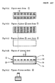
- FIG. 4-(a) One of the wiring patterns 3d on the second ceramic layer 3b in Fig. 6 of the conventional ceramic terminal part is shown schematically in Fig. 4-(a).
- the portion indicated to be resistance 1 in Fig. 4 shows the portion hidden by the third ceramic layer.
- the portion indicated to be resistance 2 in Fig. 4 shows the exposed portion that is not hidden by the third ceramic layer.
- Figure 4-(b) is a comparative example in which the width of only the portion hidden by the third ceramic layer is expanded. It is preferable for the portion hidden by the third ceramic layer to make the wiring layer thin in order to ease the heat stress produced when firing the ceramic preform and to prevent cracks in the ceramic. In this case, the only means to lower the electric resistance of the wiring layer is to have the wiring layer composed of a metal of excellent electric conductivity.
- the means for lowering the resistance of the portion hidden with the third ceramic layer in the wiring patterns is limited. If the width of the wiring pattern of the portion hidden by the third ceramic layer is made large, lowering the whole resistance is expected. However, since the distribution of current density is not uniform as shown in the case 2 of Fig. 5-(a) in fact, the resistance seldom falls compared with the conventional structure. Then, when the width of the wiring pattern is made large to the exposed portion in which the wiring pattern is not hidden with the third ceramic layer as in Fig. 4-(c), the deviation of the distribution of current density will be eased as shown in case 3 of Fig. 5-(b). Consequently, the decrease of the whole resistance becomes remarkable.
- the laminating of the material of high electrical conductivity such as silver brazing alloy and copper on the exposed portion of the wiring pattern can prevent the deviation of the distribution of current density as shown in case 6 of Fig. 5-(c).
- the resistance of the whole wiring pattern can be close to the ideal value.
- the materials with excellent thermal conductivity and with a small difference of the heat expansion coefficient of each material are used for the members of the sealed container of the present invention.
- a Cu-W alloy or a Cu-Mo alloy is used for the bottom plate on which the optical-semiconductor element is set, and an Fe-Ni-Co alloy is used for the side-frame that surrounds the area setting the optical-semiconductor element.
- Three sheets of AlN or Al 2 O 3 are used for the ceramic of the ceramic terminal part.
- Paste is prepared by adding the organic solvent to powder, such as W, Mo, and Mn, and mixing them.
- the paste containing high melting point metals is coated on the first ceramic layer which is the bottom layer and the second ceramic layer by the well-known screen printing according to the wiring pattern shown in Fig. 4-(c).
- the penetration holes are opened at the wiring pattern portion of the ceramics of the second ceramic layer, into which the high melting point metal paste is filled.
- the ceramic terminal part is formed by calcination and sintering the unified ceramic sheets with the wiring pattern consisting of high melting point metal.
- the ceiling made of Fe-Ni-Co alloy is prepared at the location that has the same level as the upper surface of the ceramic terminal part and the upper surface of the side-frame.
- the sealed airtight container for optical-semiconductors is obtained by assembling them using silver brazing and by gold plating.
- the optical-semiconductor module is obtained by sealing with a sealing cover.
- the resistance values in each wiring pattern in Fig. 4 are shown in Table 1.
- the resistance values in the case of laminating the Cu layer on the exposed electrode part and the case of pasting silver brazing on the same are also shown in Table 1.
- the resistance of the exposed electrode part is shown as resistance 2 in the wiring pattern of Fig. 4-(c).
- case 1 of the conventional structure was 10.7mohm.
- the resistance of case 2 of the comparative example that has the large width of the wiring portion hidden by the 1st ceramic layer was 9.1mohm and decreased minimally.
- Case 3 is the wiring pattern of the present invention with the large width of the exposed electrode part. The large width of the exposed part is almost equal to the width of the wiring part hidden by the third ceramic layer.
- the resistance of the case 3 was 7.0mohm, which was about 30% lower than that of the conventional structure.
- case 4 the resistance was 5.4mohm by pasting silver brazing alloy with a thickness of 10 ⁇ m on the exposed electrode part.
- the resistance of the case 4 was about half of the resistance of the conventional structure.
- the electric resistance of case 5 was 3.5mohm by laminating the copper layer of 0.1mm on the exposed electrode part.
- the electric resistance of case 6 with the copper layer of 0.2mm was 3.1mohm, which was less than 1/3 of the value of the conventional structure.
- Figure 7 is a schematic expansion view of the ceramic terminal part and the wiring part of the second example of the sealed airtight container of the present invention.
- the materials of the parts of the ceramic terminal part and the side-frame part and so forth which constituted a container were the same as that of the first example.
- the wiring patterns that were not needed to lower the resistance were formed on the second ceramic layer 3b as in the conventional structure, and the wiring patterns that were needed to lower the resistance were formed on the first ceramic layer 3a that is the bottom layer.
- W paste was painted to the required portion on the side of the second ceramic layer, and the wiring pattern was formed also on the side of the ceramic layer.
- the length of the wiring pattern becomes long in the wiring pattern of Fig. 8, since two or more layers of a wiring part can be used, a low resistance of the wiring layer is obtained. Moreover, it is also possible to lower the resistance further by preparing and laminating two or more sheets of the ceramic layer that are the same as the first ceramic layer in respect of wiring pattern.
- the ceramic terminal part was prepared by the same process as the first example, although wiring patterns are different from the first example.
- the side-frame and the bottom plate for mounting the optical-semiconductors were also prepared in the same way as the first example.
- the sealed airtight container was obtained by assembling them using silver brazing.
- the external terminal is the dumet wire structure of the Fe-Ni-Co alloy on which Cu-Ni is plated as the hardness is maintained without the decline of electric resistance.
- the optical-semiconductor module is obtained by sealing with a cover.
Landscapes
- Physics & Mathematics (AREA)
- General Physics & Mathematics (AREA)
- Optics & Photonics (AREA)
- Condensed Matter Physics & Semiconductors (AREA)
- Electromagnetism (AREA)
- Semiconductor Lasers (AREA)
- Optical Couplings Of Light Guides (AREA)
- Led Device Packages (AREA)
Abstract
Description
| Wiring pattern in Fig.4 | Resistance 1 (mΩ) | Resistance 2 (mΩ) | Whole resistance (mΩ) | | |
| Case | |||||
| 1 | Fig.4-(a) | 8.9 | 1.2 | 10.7 | |
| Case | |||||
| 2 | Fig.4-(b) | 8.9 | 1.2 | 9.1 | |
| Case | |||||
| 3 | Fig.4-(c) | 8.9 | 1.2 | 7.0 | |
| | Fig.4-(c) | 8.9 | 0.57 | 5.4 | Pasting silver |
| Case | |||||
| 5 | Fig.4-(c) | 8.9 | 0.15 | 3.5 | Laminating |
| Case | |||||
| 6 | Fig.4-(c) | 8.9 | 0.09 | 3.1 | Laminating copper layer |
Claims (6)
- A sealed airtight container comprising a bottom plate for mounting an optical-semiconductor element thereon, a side-frame, and a sealing cover, the side-frame having means for supporting a ceramic terminal part and fixing an optical fiber, wherein the width of an exposed electrode part provided in the ceramic terminal part is partially enlarged, and the enlarged portion of the exposed electrode part is connected to a wiring part provided in the ceramic terminal part, the width of the wiring part being equal to the enlarged width of the electrode part.
- A sealed airtight container according to claim 1, wherein at least two layers of a wiring part provided in a ceramic part are laminated.
- A sealed airtight container according to claim 1 or 2, wherein a silver brazing alloy is pasted on an exposed electrode part provided in a ceramic terminal part.
- A sealed airtight container according to any one of claims 1 to 3, wherein a Cu layer is laminated on an exposed electrode part provided in the ceramic terminal part.
- A sealed airtight container according to any one of claims 1 to 4, wherein an external terminal is laminated on an area where the width of the exposed electrode part is enlarged.
- An optical-semiconductor module, wherein a sealed airtight container according to claim 1 is used.
Applications Claiming Priority (2)
| Application Number | Priority Date | Filing Date | Title |
|---|---|---|---|
| JP2000266756 | 2000-09-04 | ||
| JP2000266756A JP3436243B2 (en) | 2000-09-04 | 2000-09-04 | Hermetically sealed optical semiconductor container and optical semiconductor module using the same |
Publications (2)
| Publication Number | Publication Date |
|---|---|
| EP1193770A2 true EP1193770A2 (en) | 2002-04-03 |
| EP1193770A3 EP1193770A3 (en) | 2008-12-10 |
Family
ID=18753793
Family Applications (1)
| Application Number | Title | Priority Date | Filing Date |
|---|---|---|---|
| EP01307454A Withdrawn EP1193770A3 (en) | 2000-09-04 | 2001-09-03 | Sealed airtight container for optical-semiconductors and optical-semiconductor module |
Country Status (4)
| Country | Link |
|---|---|
| US (1) | US6599034B2 (en) |
| EP (1) | EP1193770A3 (en) |
| JP (1) | JP3436243B2 (en) |
| KR (1) | KR100454208B1 (en) |
Cited By (1)
| Publication number | Priority date | Publication date | Assignee | Title |
|---|---|---|---|---|
| EP1278242A3 (en) * | 2001-06-27 | 2004-03-17 | Sumitomo Electric Industries, Ltd. | Hermetically sealing enclosure for housing photo-semiconductor devices and photo-semiconductor module incorporating the enclosure |
Families Citing this family (7)
| Publication number | Priority date | Publication date | Assignee | Title |
|---|---|---|---|---|
| US20040047571A1 (en) * | 2002-09-06 | 2004-03-11 | Boord Warren Timothy | Hermetically sealed ferrule |
| JP2012049288A (en) * | 2010-08-26 | 2012-03-08 | Kyocera Corp | Element housing package, and electronic apparatus equipped with the same |
| US8295319B2 (en) * | 2010-11-23 | 2012-10-23 | Iradion Laser, Inc. | Ceramic gas laser having an integrated beam shaping waveguide |
| US8422528B2 (en) | 2011-02-24 | 2013-04-16 | Iradion Laser, Inc. | Ceramic slab, free-space and waveguide lasers |
| US10404030B2 (en) | 2015-02-09 | 2019-09-03 | Iradion Laser, Inc. | Flat-folded ceramic slab lasers |
| CN109906534B (en) | 2016-09-20 | 2021-04-23 | 依拉迪激光有限公司 | Lasers with Recessed Apertures |
| US10297724B2 (en) * | 2017-07-10 | 2019-05-21 | Ngk Spark Plug Co., Ltd. | Package for mounting light-emitting device |
Family Cites Families (17)
| Publication number | Priority date | Publication date | Assignee | Title |
|---|---|---|---|---|
| JPS57141946A (en) * | 1981-02-27 | 1982-09-02 | Hitachi Ltd | Semiconductor device |
| JPH07138785A (en) * | 1993-11-18 | 1995-05-30 | Furukawa Electric Co Ltd:The | Optical module package |
| JP3345518B2 (en) * | 1994-09-28 | 2002-11-18 | 株式会社東芝 | Method for manufacturing optical semiconductor module |
| JPH08288588A (en) | 1995-04-18 | 1996-11-01 | Sumitomo Electric Ind Ltd | Laser diode module package |
| JPH09213838A (en) | 1996-01-31 | 1997-08-15 | Sumitomo Electric Ind Ltd | Semiconductor container terminals and semiconductor hermetically sealed container |
| JPH09237854A (en) * | 1996-02-29 | 1997-09-09 | Toshiba Corp | Semiconductor package |
| JPH09318849A (en) * | 1996-05-24 | 1997-12-12 | Fujitsu Ltd | Optical transmission module and manufacturing method thereof |
| JP4090512B2 (en) * | 1997-04-08 | 2008-05-28 | 日本オプネクスト株式会社 | Optical module |
| JP2943760B2 (en) * | 1997-04-18 | 1999-08-30 | 日本電気株式会社 | Hermetic sealing method and hermetic sealing structure for optical fiber introduction section |
| JP2993472B2 (en) | 1997-07-30 | 1999-12-20 | 住友電気工業株式会社 | Hermetically sealed container for optical semiconductor and optical semiconductor module |
| EP0899795A3 (en) * | 1997-08-27 | 1999-05-12 | Sumitomo Electric Industries, Ltd. | Optical-semiconductor container or module |
| JPH11145317A (en) | 1997-11-07 | 1999-05-28 | Sumitomo Electric Ind Ltd | Package for optical semiconductor element and optical semiconductor module |
| JP3353718B2 (en) * | 1998-09-14 | 2002-12-03 | 日本電気株式会社 | Optical communication module |
| JP3684305B2 (en) * | 1998-09-17 | 2005-08-17 | 日本オプネクスト株式会社 | Semiconductor laser coupling device and semiconductor light receiving device |
| US6123464A (en) * | 1999-02-10 | 2000-09-26 | The Furukawa Electric Co., Ltd. | Optical module package and method for manufacturing the same |
| US6420205B1 (en) * | 1999-03-24 | 2002-07-16 | Kyocera Corporation | Method for producing package for housing photosemiconductor element |
| US6440778B1 (en) * | 2000-01-07 | 2002-08-27 | The Furukawa Electric Co., Ltd. | Optical semiconductor element package and manufacturing method thereof |
-
2000
- 2000-09-04 JP JP2000266756A patent/JP3436243B2/en not_active Expired - Fee Related
-
2001
- 2001-09-03 KR KR10-2001-0053770A patent/KR100454208B1/en not_active Expired - Fee Related
- 2001-09-03 EP EP01307454A patent/EP1193770A3/en not_active Withdrawn
- 2001-09-04 US US09/944,359 patent/US6599034B2/en not_active Expired - Fee Related
Cited By (1)
| Publication number | Priority date | Publication date | Assignee | Title |
|---|---|---|---|---|
| EP1278242A3 (en) * | 2001-06-27 | 2004-03-17 | Sumitomo Electric Industries, Ltd. | Hermetically sealing enclosure for housing photo-semiconductor devices and photo-semiconductor module incorporating the enclosure |
Also Published As
| Publication number | Publication date |
|---|---|
| KR20020018962A (en) | 2002-03-09 |
| EP1193770A3 (en) | 2008-12-10 |
| US20020051610A1 (en) | 2002-05-02 |
| JP2002076499A (en) | 2002-03-15 |
| JP3436243B2 (en) | 2003-08-11 |
| US6599034B2 (en) | 2003-07-29 |
| KR100454208B1 (en) | 2004-10-26 |
Similar Documents
| Publication | Publication Date | Title |
|---|---|---|
| US5111277A (en) | Surface mount device with high thermal conductivity | |
| US5188985A (en) | Surface mount device with high thermal conductivity | |
| US20040183172A1 (en) | Package for housing semiconductor chip, and semiconductor device | |
| JPH05206356A (en) | Package for integrated circuit | |
| EP1193770A2 (en) | Sealed airtight container for optical-semiconductors and optical-semiconductor module | |
| CN108962846A (en) | A kind of encapsulating structure of thick film hybrid integrated circuit and preparation method thereof | |
| KR20030060891A (en) | Optical semiconductor module and method of producing the same | |
| US6600223B2 (en) | Hermetically sealing enclosure for housing photo-semiconductor devices and photo-semiconductor module incorporating the enclosure | |
| JP4771588B2 (en) | Optical semiconductor element storage package | |
| JP2004356391A (en) | Semiconductor element storage package and semiconductor device | |
| JPH06314747A (en) | Package for storing optical semiconductor elements | |
| JP2007012706A (en) | Electronic component storage package and electronic device | |
| JP3615697B2 (en) | Package for storing semiconductor elements | |
| CN1331217C (en) | Chip package structure and its substrate | |
| JP2003197803A (en) | Semiconductor package | |
| JP2543149Y2 (en) | Package for storing semiconductor elements | |
| JP4497762B2 (en) | Optical semiconductor element storage package and optical semiconductor device | |
| JP2003318451A (en) | Thermoelectric element module, semiconductor element storage package and semiconductor module | |
| JP4018964B2 (en) | Package for housing input/output terminals and semiconductor elements | |
| JP2525232B2 (en) | Ceramic package and method of manufacturing the same | |
| JP2004221505A (en) | Optical semiconductor element storage package and optical semiconductor device | |
| JP2005191140A (en) | Electronic component storage package and electronic device | |
| JP2003197987A (en) | Thermoelectric element module, semiconductor element storage package and semiconductor module | |
| JP2003152231A (en) | Thermoelectric element module, semiconductor element storage package and semiconductor module | |
| JP2012138437A (en) | Electronic component housing package |
Legal Events
| Date | Code | Title | Description |
|---|---|---|---|
| PUAI | Public reference made under article 153(3) epc to a published international application that has entered the european phase |
Free format text: ORIGINAL CODE: 0009012 |
|
| AK | Designated contracting states |
Kind code of ref document: A2 Designated state(s): AT BE CH CY DE DK ES FI FR GB GR IE IT LI LU MC NL PT SE TR |
|
| AX | Request for extension of the european patent |
Free format text: AL;LT;LV;MK;RO;SI |
|
| PUAL | Search report despatched |
Free format text: ORIGINAL CODE: 0009013 |
|
| AK | Designated contracting states |
Kind code of ref document: A3 Designated state(s): AT BE CH CY DE DK ES FI FR GB GR IE IT LI LU MC NL PT SE TR |
|
| AX | Request for extension of the european patent |
Extension state: AL LT LV MK RO SI |
|
| AKX | Designation fees paid | ||
| REG | Reference to a national code |
Ref country code: DE Ref legal event code: 8566 |
|
| STAA | Information on the status of an ep patent application or granted ep patent |
Free format text: STATUS: THE APPLICATION IS DEEMED TO BE WITHDRAWN |
|
| 18D | Application deemed to be withdrawn |
Effective date: 20090611 |