EP1193752A1 - Method to form a localized silicon-on-insulator structure - Google Patents
Method to form a localized silicon-on-insulator structure Download PDFInfo
- Publication number
- EP1193752A1 EP1193752A1 EP00402680A EP00402680A EP1193752A1 EP 1193752 A1 EP1193752 A1 EP 1193752A1 EP 00402680 A EP00402680 A EP 00402680A EP 00402680 A EP00402680 A EP 00402680A EP 1193752 A1 EP1193752 A1 EP 1193752A1
- Authority
- EP
- European Patent Office
- Prior art keywords
- layer
- substrate
- single crystal
- dielectric material
- semiconductor
- Prior art date
- Legal status (The legal status is an assumption and is not a legal conclusion. Google has not performed a legal analysis and makes no representation as to the accuracy of the status listed.)
- Withdrawn
Links
Images


Classifications
-
- H—ELECTRICITY
- H10—SEMICONDUCTOR DEVICES; ELECTRIC SOLID-STATE DEVICES NOT OTHERWISE PROVIDED FOR
- H10P—GENERIC PROCESSES OR APPARATUS FOR THE MANUFACTURE OR TREATMENT OF DEVICES COVERED BY CLASS H10
- H10P14/00—Formation of materials, e.g. in the shape of layers or pillars
- H10P14/20—Formation of materials, e.g. in the shape of layers or pillars of semiconductor materials
- H10P14/24—Formation of materials, e.g. in the shape of layers or pillars of semiconductor materials using chemical vapour deposition [CVD]
-
- H—ELECTRICITY
- H10—SEMICONDUCTOR DEVICES; ELECTRIC SOLID-STATE DEVICES NOT OTHERWISE PROVIDED FOR
- H10P—GENERIC PROCESSES OR APPARATUS FOR THE MANUFACTURE OR TREATMENT OF DEVICES COVERED BY CLASS H10
- H10P14/00—Formation of materials, e.g. in the shape of layers or pillars
- H10P14/20—Formation of materials, e.g. in the shape of layers or pillars of semiconductor materials
- H10P14/38—Formation of materials, e.g. in the shape of layers or pillars of semiconductor materials characterised by treatments done after the formation of the materials
- H10P14/3802—Crystallisation or recrystallisation of non-monocrystalline semiconductor materials, e.g. regrowth
-
- H—ELECTRICITY
- H10—SEMICONDUCTOR DEVICES; ELECTRIC SOLID-STATE DEVICES NOT OTHERWISE PROVIDED FOR
- H10P—GENERIC PROCESSES OR APPARATUS FOR THE MANUFACTURE OR TREATMENT OF DEVICES COVERED BY CLASS H10
- H10P14/00—Formation of materials, e.g. in the shape of layers or pillars
- H10P14/20—Formation of materials, e.g. in the shape of layers or pillars of semiconductor materials
- H10P14/29—Formation of materials, e.g. in the shape of layers or pillars of semiconductor materials characterised by the substrates
- H10P14/2901—Materials
- H10P14/2902—Materials being Group IVA materials
- H10P14/2905—Silicon, silicon germanium or germanium
-
- H—ELECTRICITY
- H10—SEMICONDUCTOR DEVICES; ELECTRIC SOLID-STATE DEVICES NOT OTHERWISE PROVIDED FOR
- H10P—GENERIC PROCESSES OR APPARATUS FOR THE MANUFACTURE OR TREATMENT OF DEVICES COVERED BY CLASS H10
- H10P14/00—Formation of materials, e.g. in the shape of layers or pillars
- H10P14/20—Formation of materials, e.g. in the shape of layers or pillars of semiconductor materials
- H10P14/29—Formation of materials, e.g. in the shape of layers or pillars of semiconductor materials characterised by the substrates
- H10P14/2926—Crystal orientations
-
- H—ELECTRICITY
- H10—SEMICONDUCTOR DEVICES; ELECTRIC SOLID-STATE DEVICES NOT OTHERWISE PROVIDED FOR
- H10P—GENERIC PROCESSES OR APPARATUS FOR THE MANUFACTURE OR TREATMENT OF DEVICES COVERED BY CLASS H10
- H10P14/00—Formation of materials, e.g. in the shape of layers or pillars
- H10P14/20—Formation of materials, e.g. in the shape of layers or pillars of semiconductor materials
- H10P14/32—Formation of materials, e.g. in the shape of layers or pillars of semiconductor materials characterised by intermediate layers between substrates and deposited layers
- H10P14/3202—Materials thereof
- H10P14/3204—Materials thereof being Group IVA semiconducting materials
- H10P14/3211—Silicon, silicon germanium or germanium
-
- H—ELECTRICITY
- H10—SEMICONDUCTOR DEVICES; ELECTRIC SOLID-STATE DEVICES NOT OTHERWISE PROVIDED FOR
- H10P—GENERIC PROCESSES OR APPARATUS FOR THE MANUFACTURE OR TREATMENT OF DEVICES COVERED BY CLASS H10
- H10P14/00—Formation of materials, e.g. in the shape of layers or pillars
- H10P14/20—Formation of materials, e.g. in the shape of layers or pillars of semiconductor materials
- H10P14/32—Formation of materials, e.g. in the shape of layers or pillars of semiconductor materials characterised by intermediate layers between substrates and deposited layers
- H10P14/3202—Materials thereof
- H10P14/3238—Materials thereof being insulating materials
-
- H—ELECTRICITY
- H10—SEMICONDUCTOR DEVICES; ELECTRIC SOLID-STATE DEVICES NOT OTHERWISE PROVIDED FOR
- H10P—GENERIC PROCESSES OR APPARATUS FOR THE MANUFACTURE OR TREATMENT OF DEVICES COVERED BY CLASS H10
- H10P14/00—Formation of materials, e.g. in the shape of layers or pillars
- H10P14/20—Formation of materials, e.g. in the shape of layers or pillars of semiconductor materials
- H10P14/32—Formation of materials, e.g. in the shape of layers or pillars of semiconductor materials characterised by intermediate layers between substrates and deposited layers
- H10P14/3242—Structure
- H10P14/3244—Layer structure
- H10P14/3248—Layer structure consisting of two layers
-
- H—ELECTRICITY
- H10—SEMICONDUCTOR DEVICES; ELECTRIC SOLID-STATE DEVICES NOT OTHERWISE PROVIDED FOR
- H10P—GENERIC PROCESSES OR APPARATUS FOR THE MANUFACTURE OR TREATMENT OF DEVICES COVERED BY CLASS H10
- H10P14/00—Formation of materials, e.g. in the shape of layers or pillars
- H10P14/20—Formation of materials, e.g. in the shape of layers or pillars of semiconductor materials
- H10P14/34—Deposited materials, e.g. layers
- H10P14/3402—Deposited materials, e.g. layers characterised by the chemical composition
- H10P14/3404—Deposited materials, e.g. layers characterised by the chemical composition being Group IVA materials
- H10P14/3411—Silicon, silicon germanium or germanium
-
- H—ELECTRICITY
- H10—SEMICONDUCTOR DEVICES; ELECTRIC SOLID-STATE DEVICES NOT OTHERWISE PROVIDED FOR
- H10P—GENERIC PROCESSES OR APPARATUS FOR THE MANUFACTURE OR TREATMENT OF DEVICES COVERED BY CLASS H10
- H10P14/00—Formation of materials, e.g. in the shape of layers or pillars
- H10P14/20—Formation of materials, e.g. in the shape of layers or pillars of semiconductor materials
- H10P14/34—Deposited materials, e.g. layers
- H10P14/3451—Structure
- H10P14/3452—Microstructure
- H10P14/3458—Monocrystalline
-
- H—ELECTRICITY
- H10—SEMICONDUCTOR DEVICES; ELECTRIC SOLID-STATE DEVICES NOT OTHERWISE PROVIDED FOR
- H10P—GENERIC PROCESSES OR APPARATUS FOR THE MANUFACTURE OR TREATMENT OF DEVICES COVERED BY CLASS H10
- H10P90/00—Preparation of wafers not covered by a single main group of this subclass, e.g. wafer reinforcement
- H10P90/19—Preparing inhomogeneous wafers
- H10P90/1904—Preparing vertically inhomogeneous wafers
- H10P90/1906—Preparing SOI wafers
- H10P90/1912—Preparing SOI wafers using selective deposition, e.g. epitaxial lateral overgrowth [ELO] or selective deposition of single crystal silicon
-
- H—ELECTRICITY
- H10—SEMICONDUCTOR DEVICES; ELECTRIC SOLID-STATE DEVICES NOT OTHERWISE PROVIDED FOR
- H10W—GENERIC PACKAGES, INTERCONNECTIONS, CONNECTORS OR OTHER CONSTRUCTIONAL DETAILS OF DEVICES COVERED BY CLASS H10
- H10W10/00—Isolation regions in semiconductor bodies between components of integrated devices
- H10W10/01—Manufacture or treatment
- H10W10/031—Manufacture or treatment of isolation regions comprising PN junctions
-
- H—ELECTRICITY
- H10—SEMICONDUCTOR DEVICES; ELECTRIC SOLID-STATE DEVICES NOT OTHERWISE PROVIDED FOR
- H10W—GENERIC PACKAGES, INTERCONNECTIONS, CONNECTORS OR OTHER CONSTRUCTIONAL DETAILS OF DEVICES COVERED BY CLASS H10
- H10W10/00—Isolation regions in semiconductor bodies between components of integrated devices
- H10W10/10—Isolation regions comprising dielectric materials
- H10W10/181—Semiconductor-on-insulator [SOI] isolation regions, e.g. buried oxide regions of SOI wafers
-
- H—ELECTRICITY
- H10—SEMICONDUCTOR DEVICES; ELECTRIC SOLID-STATE DEVICES NOT OTHERWISE PROVIDED FOR
- H10W—GENERIC PACKAGES, INTERCONNECTIONS, CONNECTORS OR OTHER CONSTRUCTIONAL DETAILS OF DEVICES COVERED BY CLASS H10
- H10W10/00—Isolation regions in semiconductor bodies between components of integrated devices
- H10W10/30—Isolation regions comprising PN junctions
Definitions
- This invention relates to lateral epitaxial growth over oxide, a known process (usually referred to by the acronym LEGO) in semiconductor manufacture.
- the LEGO method conventionally requires melting of the whole surface of a wafer, including both SOI and non-SOI areas. Clearly, melting of the non-SOI areas is undesirable and may compromise the functionality of the power components.
- a semiconductor device fabricated by lateral epitaxial growth over oxide as claimed in claim 1.
- the structure 100 is formed from a substrate of starting material 1, which is preferably comprised of silicon.
- the substrate 1 is of a ⁇ 100> crystal orientation.
- a dielectric layer 2 for example of thermal oxide
- the thermal oxidation process comprises successive dry, wet and dry stages, resulting in a stack of successive individual oxide layers which together constitute the oxide layer 2.
- the dry deposition steps provide good insulation capabilities to the oxide layer, and the wet deposition step permits an increase in the process deposition rate.
- oxide layer 2 is of the order of 1 to 2 micron thick, and is deposited at approximately 1,150°C with a growth rate of approximately 30 Angstroms/minute.
- a thin polycrystalline semiconductor layer 6 is formed over the thermal oxide layer 2.
- the thin polycrystalline semiconductor layer 6 is deposited by low pressure chemical vapor deposition (LPCVD).
- LPCVD low pressure chemical vapor deposition
- the polycrystalline layer 6 is preferably undoped polysilicon, deposited using silane at approximately 600°C with a growth rate of 100 Angströms/minute.
- the polysilicon layer 6 is approximately 3000 Angstroms thick.
- a photoresist layer 7 is deposited onto the polycrystalline semiconductor layer 6 using standard photoresist dispensing techniques.
- the photoresist layer 7 is a positive photoresist such as AZ 1529 containing 2-Methoxy-1-methylethylacetate from Clariant GmbH of Germany.
- the layer is soft baked at a low temperature to dehydrate and remove excess solvents.
- the photoresist layer 7 is selectively exposed to light using a photomask (not shown).
- the photoresist layer 7 is developed in order to selectively remove photoresist from the layer 7 to form a desired pattern.
- a developer containing sodium metasilicate such as AZ developer from Clariant GmbH of Germany is used. Then the developed photoresist layer 7 is soft baked at a higher temperature.
- the polycrystalline semiconductor layer 6 is etched to conform to the pattern provided by the remaining photoresist layer 7.
- the polysilicon layer 6 is etched using a reactive ion etch (RIE) system.
- RIE reactive ion etch
- the thermal oxide layer 2 is chemically etched.
- the thermal oxide film 2 is etched to conform to the pattern provided by the remaining photoresist layer 7, using a chemical etchant solution containing ammonium fluoride and hydrofluoric acid from Merck S.A. for example.
- the etched oxide layer 2 thus has left and right edges which are laterally inwardly spaced from the edges of the substrate and which define an exposed area (on left and right) between the oxide layer 2 and the edges of the substrate 1.
- the remaining photoresist layer 7 is removed, as shown in FIG. 9, using a conventional solvent etchant.
- the substrate 1 is then rinsed using de-ionized water and dried.
- a thick semiconductor layer (9 and 1') is deposited over the entire structure surface.
- the thick semiconductor layer (9 and 1') is deposited using epitaxial growth and is of the order of 10 to 30 microns thick.
- the thick semiconductor layer (9 and 1') is deposited using trichlorosilane at approximately 1,110°C at atmospheric pressure with a growth rate of approximately 1.5 micron/minute.
- the semiconductor layer (9 and 1') deposited by epitaxial growth is preferably of the same conductivity type as the substrate 1 and with the same doping.
- the epitaxial growth over the polycrystalline semiconductor layer 6 gives a polycrystalline area 9, and over the substrate 1 the epitaxial growth gives a single crystal zone 1'.
- the present invention provides more particularly two different regions: the polycrystalline zone 9 and the single crystal zone 1'.
- an oxide film 10 is deposited by low pressure chemical vapor deposition (LPCVD), using silane and oxygen at approximately 340°C with a growth rate of approximately 300 Angströms/minute.
- the oxide layer 10 is of the order of 1 to 2 microns thick.
- the substrate 1 is placed into a rapid thermal reactor. Using a vertical thermal gradient, the polycrystalline area 9 over the oxide layer 2 is melted at approximately 1,412°C and recrystallized during the freezing step of rapid thermal annealing. It is to be noted that rapid thermal annealing affects only the polycrystalline zone 9 localized over the oxide layer 2 without modifying the single crystal area 1'. The single crystal zone 1' over the substrate 1 is not melted. The rapid thermal annealing provides a single crystal zone 3 over the oxide layer 2.
- the cap oxide layer 10 is removed using a chemical wet etch such as hydrofluoric acid etch.
- the semiconductor layer 3 is planarized using a chemical-mechanical-polishing. After planarization, semiconductor material 3 with a thickness of the order of 5 to 20 microns thick is left over the oxide layer 2.
- the SOI structure is then subjected to a diffusion process in which the deep junction diffusion or trench regions 4 and 5 are formed, extending from the top surface to left and right edges of the oxide layer 2, to produce the structure shown in FIG. 1. It will be appreciated that the region between the oxide layer 2 and the diffusion regions 4 and 5 is dielectrically isolated from the remainder of the substrate and may therefore be used to provide control circuitry for power components in the remainder of the substrate.
Landscapes
- Element Separation (AREA)
Abstract
A semiconductor device and method of fabrication using
LEGO (Lateral Epitaxial Growth over Oxide) for forming a
SOI (Silicon On Insulator) structure (FIG. 1) having a
localized buried dielectric layer (2). By patterning the
buried dielectric layer, covered with a thin polysilicon
layer by way of an epitaxial reactor a thick
semiconductor layer (3) over the buried layer (2) is
deposited. By rapid thermal annealing the polycrystalline
overlayer is transformed into a single crystal layer (3).
The buried oxide layer (2) provides a vertical
dielectrical insulation, and deep diffused or trench
regions (4, 5) provide lateral junction insulation. In
this manner the SOI area (3) localized between the two
deep diffused regions (4, 5) is fully insulated from the
silicon substrate (1). This provides the following
advantages: the process can be easily integrated in
standard wafer fabrication equipment and processing
techniques; the process is fully compatible with many
existing technologies and their process flow; and low
processing cost and low density defectivity should
result.
Description
- This invention relates to lateral epitaxial growth over oxide, a known process (usually referred to by the acronym LEGO) in semiconductor manufacture.
- In the field of this invention it is known to use the lateral epitaxial growth over oxide (LEGO) method to form a localized silicon-on-insulator (SOI) structure, at low cost, with thick silicon and insulator films. Typically, in the field of Smart Power applications (i.e., semiconductor devices combining both high power functions and low voltage/power control functions), the non-SOI areas are devoted to vertical power components and the localized SOI structure provides isolation for the power components' control circuitry.
- However, the LEGO method conventionally requires melting of the whole surface of a wafer, including both SOI and non-SOI areas. Clearly, melting of the non-SOI areas is undesirable and may compromise the functionality of the power components.
- These problems may be avoided by use of other known techniques such as SIMOX and direct wafer bonding, but these require very expensive processing steps (e.g., high temperature and high dosage O2 implants followed by multiple anneal cycles for SIMOX, and the joining and bonding of two substrate wafers for direct wafer bonding).
- It is an object of the present invention to provide a semiconductor device and method of manufacture using lateral epitaxial growth over oxide wherein the abovementioned disadvantage(s) may be alleviated.
- In accordance with a first aspect of the present invention there is provided a semiconductor device fabricated by lateral epitaxial growth over oxide as claimed in
claim 1. - In accordance with a second aspect of the present invention there is provided a method of fabricating a semiconductor device by lateral epitaxial growth over oxide as claimed in
claim 7. - One semiconductor device and method of manufacture by lateral epitaxial growth over oxide incorporating the present invention will now be described, by way of example only, with reference to the accompanying drawing(s), in which:
- FIG. 1 is a cross-sectional view of a SOI structure incorporating the present invention; and
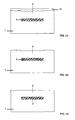
- FIGS. 2-14 are cross-sectional views illustrating successive stages during fabrication of the device of FIG. 1.
-
- Referring now to FIG. 2, the structure 100 is formed from a substrate of starting
material 1, which is preferably comprised of silicon. Preferably, thesubstrate 1 is of a <100> crystal orientation. - As shown in FIG. 3, at an early stage of fabrication a
dielectric layer 2, for example of thermal oxide, is formed over the surface of the substrate. The thermal oxidation process comprises successive dry, wet and dry stages, resulting in a stack of successive individual oxide layers which together constitute theoxide layer 2. The dry deposition steps provide good insulation capabilities to the oxide layer, and the wet deposition step permits an increase in the process deposition rate. Generally,oxide layer 2 is of the order of 1 to 2 micron thick, and is deposited at approximately 1,150°C with a growth rate of approximately 30 Angstroms/minute. - As shown in FIG. 4, at a later stage of fabrication a thin
polycrystalline semiconductor layer 6 is formed over thethermal oxide layer 2. The thinpolycrystalline semiconductor layer 6 is deposited by low pressure chemical vapor deposition (LPCVD). Thepolycrystalline layer 6 is preferably undoped polysilicon, deposited using silane at approximately 600°C with a growth rate of 100 Angströms/minute. Thepolysilicon layer 6 is approximately 3000 Angstroms thick. - As shown in FIG. 5, at a further stage of fabrication a
photoresist layer 7 is deposited onto thepolycrystalline semiconductor layer 6 using standard photoresist dispensing techniques. Preferably, thephotoresist layer 7 is a positive photoresist such as AZ 1529 containing 2-Methoxy-1-methylethylacetate from Clariant GmbH of Germany. After thephotoresist layer 7 is deposited, the layer is soft baked at a low temperature to dehydrate and remove excess solvents. Next, thephotoresist layer 7 is selectively exposed to light using a photomask (not shown). - As shown in FIG. 6, after exposure, the
photoresist layer 7 is developed in order to selectively remove photoresist from thelayer 7 to form a desired pattern. To develop positive photoresist, a developer containing sodium metasilicate such as AZ developer from Clariant GmbH of Germany is used. Then the developedphotoresist layer 7 is soft baked at a higher temperature. - Next, as shown in FIG. 7, the
polycrystalline semiconductor layer 6 is etched to conform to the pattern provided by the remainingphotoresist layer 7. Thepolysilicon layer 6 is etched using a reactive ion etch (RIE) system. - As shown in FIG. 8, after the
polycrystalline semiconductor layer 6 is etched, thethermal oxide layer 2 is chemically etched. Thethermal oxide film 2 is etched to conform to the pattern provided by the remainingphotoresist layer 7, using a chemical etchant solution containing ammonium fluoride and hydrofluoric acid from Merck S.A. for example. As can be seen in FIG. 8, theetched oxide layer 2 thus has left and right edges which are laterally inwardly spaced from the edges of the substrate and which define an exposed area (on left and right) between theoxide layer 2 and the edges of thesubstrate 1. - The remaining
photoresist layer 7 is removed, as shown in FIG. 9, using a conventional solvent etchant. Thesubstrate 1 is then rinsed using de-ionized water and dried. - As shown in FIG. 10, a thick semiconductor layer (9 and 1') is deposited over the entire structure surface. The thick semiconductor layer (9 and 1') is deposited using epitaxial growth and is of the order of 10 to 30 microns thick. Preferably, the thick semiconductor layer (9 and 1') is deposited using trichlorosilane at approximately 1,110°C at atmospheric pressure with a growth rate of approximately 1.5 micron/minute. The semiconductor layer (9 and 1') deposited by epitaxial growth is preferably of the same conductivity type as the
substrate 1 and with the same doping. As shown in FIG. 10, the epitaxial growth over thepolycrystalline semiconductor layer 6 gives apolycrystalline area 9, and over thesubstrate 1 the epitaxial growth gives a single crystal zone 1'. The present invention provides more particularly two different regions: thepolycrystalline zone 9 and the single crystal zone 1'. - As shown in FIG. 11, at a later stage in fabrication, after the epitaxial growth of the
semiconductor layer 9 over theoxide layer 2, anoxide film 10 is deposited by low pressure chemical vapor deposition (LPCVD), using silane and oxygen at approximately 340°C with a growth rate of approximately 300 Angströms/minute. Theoxide layer 10 is of the order of 1 to 2 microns thick. - As shown in FIG. 12, in the final stages of fabrication, after the deposition of the
cap oxide layer 10, thesubstrate 1 is placed into a rapid thermal reactor. Using a vertical thermal gradient, thepolycrystalline area 9 over theoxide layer 2 is melted at approximately 1,412°C and recrystallized during the freezing step of rapid thermal annealing. It is to be noted that rapid thermal annealing affects only thepolycrystalline zone 9 localized over theoxide layer 2 without modifying the single crystal area 1'. The single crystal zone 1' over thesubstrate 1 is not melted. The rapid thermal annealing provides asingle crystal zone 3 over theoxide layer 2. - As shown in FIG. 13, the
cap oxide layer 10 is removed using a chemical wet etch such as hydrofluoric acid etch. - As shown in FIG. 14, at the end of fabrication, the
semiconductor layer 3 is planarized using a chemical-mechanical-polishing. After planarization,semiconductor material 3 with a thickness of the order of 5 to 20 microns thick is left over theoxide layer 2. - The SOI structure is then subjected to a diffusion process in which the deep junction diffusion or
trench regions oxide layer 2, to produce the structure shown in FIG. 1. It will be appreciated that the region between theoxide layer 2 and thediffusion regions - It will be understood that the semiconductor device and method of manufacture using lateral epitaxial growth over oxide described above provides the following advantages:
- the process can be easily integrated in standard wafer fabrication equipment and processing techniques;
- the process is fully compatible with CMOS, Smartmos, SmartPower and analog technologies and their process flow; and
- low processing cost and low density defectivity should result.
Claims (14)
- A semiconductor device fabricated by lateral epitaxial growth over oxide, comprising:a substrate (1) of semiconductor material having a predetermined conductivity type and a predetermined doping;a layer (2) of dielectric material extending laterally within the substrate, the layer of dielectric material having a lateral edge remote from an adjacent edge of the substrate; andan epitaxially grown layer of single crystal semiconductor material extending laterally across the substrate and extending perpendicularly from the layer of dielectric material, the layer of single crystal semiconductor material having:a first single crystal portion (1') overlying the area between the lateral edge of the layer of dielectric material and the adjacent edge of the substrate, anda second single crystal portion (9) overlying the layer of dielectric material and formed from re-crystallisation of polycrystalline material without melting of the first portion.
- The semiconductor device according to claim 1, wherein the layer (2) of dielectric material comprises oxide.
- The semiconductor device according to claim 2, wherein the layer (2) of dielectric material comprises stacked layers of oxide.
- The semiconductor device according to claim 1, 2 or 3, wherein the layer of single crystal material is of semiconductor material having the same conductivity type and the same doping as the substrate.
- The semiconductor device according to claim 1, 2, 3 or 4, further comprising first (4) and second (5) deep diffusion regions extending through the layer of single crystal material from a surface of the substrate to respective separated parts of the layer of dielectric material.
- The semiconductor device according to any preceding claim wherein the semiconductor material of the substrate (1) and of the layer of single crystal material is silicon.
- A method of fabricating a semiconductor device by lateral epitaxial growth over oxide, comprising:providing a substrate (1) of semiconductor material having a predetermined conductivity type and a predetermined doping;providing a layer (2) of dielectric material extending laterally within the substrate, the layer of dielectric material having a lateral edge remote from an adjacent edge of the substrate; andgrowing an epitaxial layer of crystalline semiconductor material extending laterally across the substrate and extending perpendicularly from the layer of dielectric material, the layer of crystalline semiconductor material having:a first portion (1') of single crystal material overlying the area between the lateral edge of the layer of dielectric material and the adjacent edge of the substrate, anda second portion (9) of polycrystalline material overlying the layer of dielectric material; andre-crystallising the second portion (9) of polycrystalline material into single crystal material without melting of the first portion of single crystal material.
- The method according to claim 7, wherein the step of providing the layer (2) of dielectric material comprises growing a layer of thermal oxide.
- The method according to claim 7 or 8, wherein the step of re-crystallising the second portion (9) of polycrystalline material into single crystal material without melting of the first portion of single crystal material comprises rapid thermal annealing.
- The method according to claim 9, wherein the rapid thermal annealing utilizes a thermal gradient in a direction perpendicular to the direction of lateral extension.
- The method according to any one of claims 7-10, wherein the step of providing a layer of dielectric material comprises:providing a layer (6) of dielectric material extending laterally across the substrate; andpatterning the dielectric layer by photoresistive etching (7) to define the area between the lateral edge of the layer of dielectric material and the adjacent edge of the substrate.
- The method according to any one of claims 7-11, wherein the layer of crystalline material is of semiconductor material having the same conductivity type and the same doping as the substrate.
- The method according to any one of claims 7-12, further comprising providing first (4) and second (5) deep diffusion regions extending through the layer of single crystal material from a surface of the substrate to respective separated parts of the layer (2) of dielectric material to provide dielectric isolation of the region therebetween.
- The method according to any one of claims 7-13, wherein the semiconductor material of the substrate and of the layer of single crystal material is silicon.
Priority Applications (1)
| Application Number | Priority Date | Filing Date | Title |
|---|---|---|---|
| EP00402680A EP1193752A1 (en) | 2000-09-28 | 2000-09-28 | Method to form a localized silicon-on-insulator structure |
Applications Claiming Priority (1)
| Application Number | Priority Date | Filing Date | Title |
|---|---|---|---|
| EP00402680A EP1193752A1 (en) | 2000-09-28 | 2000-09-28 | Method to form a localized silicon-on-insulator structure |
Publications (1)
| Publication Number | Publication Date |
|---|---|
| EP1193752A1 true EP1193752A1 (en) | 2002-04-03 |
Family
ID=8173883
Family Applications (1)
| Application Number | Title | Priority Date | Filing Date |
|---|---|---|---|
| EP00402680A Withdrawn EP1193752A1 (en) | 2000-09-28 | 2000-09-28 | Method to form a localized silicon-on-insulator structure |
Country Status (1)
| Country | Link |
|---|---|
| EP (1) | EP1193752A1 (en) |
Cited By (2)
| Publication number | Priority date | Publication date | Assignee | Title |
|---|---|---|---|---|
| EP1398825A3 (en) * | 2002-09-11 | 2010-04-28 | Canon Kabushiki Kaisha | Substrate and manufacturing method therefor |
| US8344453B2 (en) | 2007-10-18 | 2013-01-01 | Nxp B.V. | Method of manufacturing localized semiconductor-on-insulator (SOI) structures in a bulk semiconductor wafer |
Citations (1)
| Publication number | Priority date | Publication date | Assignee | Title |
|---|---|---|---|---|
| EP0147626A2 (en) * | 1983-11-24 | 1985-07-10 | Hitachi, Ltd. | Semiconductor device comprising bipolar and MOS transistors, and method of producing the same |
-
2000
- 2000-09-28 EP EP00402680A patent/EP1193752A1/en not_active Withdrawn
Patent Citations (1)
| Publication number | Priority date | Publication date | Assignee | Title |
|---|---|---|---|---|
| EP0147626A2 (en) * | 1983-11-24 | 1985-07-10 | Hitachi, Ltd. | Semiconductor device comprising bipolar and MOS transistors, and method of producing the same |
Non-Patent Citations (1)
| Title |
|---|
| DILHAC J -M ET AL: "USE OF RAPID THERMAL PROCESSING FOR ISOLATION AND INTERCONNECT TECHNOLOGIES APPLIED TO SMART POWER", EPE. EUROPEAN CONFERENCE ON POWER ELECTRONICS AND APPLICATIONS,B,BRUSSELS, EPE ASSOCIATION, vol. CONF. 7, 8 September 1997 (1997-09-08), pages 3009 - 3014, XP000768256, ISBN: 90-75815-02-6 * |
Cited By (2)
| Publication number | Priority date | Publication date | Assignee | Title |
|---|---|---|---|---|
| EP1398825A3 (en) * | 2002-09-11 | 2010-04-28 | Canon Kabushiki Kaisha | Substrate and manufacturing method therefor |
| US8344453B2 (en) | 2007-10-18 | 2013-01-01 | Nxp B.V. | Method of manufacturing localized semiconductor-on-insulator (SOI) structures in a bulk semiconductor wafer |
Similar Documents
| Publication | Publication Date | Title |
|---|---|---|
| US6211039B1 (en) | Silicon-on-insulator islands and method for their formation | |
| US6096433A (en) | Laminated substrate fabricated from semiconductor wafers bonded to each other without contact between insulating layer and semiconductor layer and process of fabrication thereof | |
| US6159822A (en) | Self-planarized shallow trench isolation | |
| JPH0580148B2 (en) | ||
| US4851366A (en) | Method for providing dielectrically isolated circuit | |
| WO1988005600A1 (en) | Process for producing thin single crystal silicon islands on insulator | |
| US6127244A (en) | Method of manufacturing semiconductor device | |
| US4891092A (en) | Method for making a silicon-on-insulator substrate | |
| US6171929B1 (en) | Shallow trench isolator via non-critical chemical mechanical polishing | |
| US7067387B2 (en) | Method of manufacturing dielectric isolated silicon structure | |
| EP0488344A2 (en) | SOI wafer fabrication by selective epitaxial growth | |
| KR100293009B1 (en) | Method of manufacturing semiconductor device | |
| US6613639B1 (en) | Forming a semiconductor on implanted insulator | |
| JPH06232247A (en) | Method for manufacturing an isolated semiconductor layer on an insulating layer | |
| JPH0974189A (en) | Method for manufacturing semiconductor device | |
| JP2839088B2 (en) | Semiconductor device | |
| US20060115935A1 (en) | Method of manufacturing semiconductor substrate and method of manufacturing semiconductor device | |
| JP3321527B2 (en) | Method for manufacturing semiconductor device | |
| JPH02260442A (en) | Dielectric isolation type semiconductor substrate | |
| KR940009355B1 (en) | Semiconductor device and manufacturing method thereof | |
| KR100289658B1 (en) | Semiconductor Device Separation Method | |
| JP3270912B2 (en) | Method for manufacturing semiconductor device | |
| KR100308420B1 (en) | Shallow trench etching method for isolating semiconductor devices | |
| JPS60189235A (en) | Production of semiconductor device | |
| KR100204911B1 (en) | Manufacturing method of plug in semiconductor device |
Legal Events
| Date | Code | Title | Description |
|---|---|---|---|
| PUAI | Public reference made under article 153(3) epc to a published international application that has entered the european phase |
Free format text: ORIGINAL CODE: 0009012 |
|
| AK | Designated contracting states |
Kind code of ref document: A1 Designated state(s): AT BE CH CY DE DK ES FI FR GB GR IE IT LI LU MC NL PT SE |
|
| AX | Request for extension of the european patent |
Free format text: AL;LT;LV;MK;RO;SI |
|
| AKX | Designation fees paid | ||
| REG | Reference to a national code |
Ref country code: DE Ref legal event code: 8566 |
|
| STAA | Information on the status of an ep patent application or granted ep patent |
Free format text: STATUS: THE APPLICATION IS DEEMED TO BE WITHDRAWN |
|
| 18D | Application deemed to be withdrawn |
Effective date: 20021005 |