FIELD OF THE INVENTION
The present invention relates to an annealing
method for an SOI substrate having a semiconductor
layer such as a silicon layer formed on an insulator,
in which the number of defects (HF defects) in an SOI
layer (the semiconductor layer on the insulator) and,
more specifically, the number of HF defects which
increase as an SOI layer becomes thin is reduced by
annealing the SOI substrate in a reducing gas
atmosphere, and an SOI substrate using the annealing
method.
BACKGROUND OF THE INVENTION
Sato et al. has reported a technique of annealing
an SOI (Semiconductor On Insulator) wafer in a reducing
atmosphere, in which, e.g., annealing in hydrogen gas
at 1,000°C yields so high planarity that the roughness
on an SOI layer surface is 2 nm or less (Japanese
Patent Laid-Open No. 05-217821 and U.S. Patent
No. 5,371,037).
This technique will be described with reference
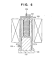
to Figs. 6 and 7. An example using a vertical
annealing furnace is shown in Fig. 6.
Referring to Fig. 6, reference numeral 101
denotes a furnace tube serving as a reactor. An
atmospheric gas is supplied from a supply pipe 102
arranged at the upper portion and exhausted from an
exhaust pipe 103 at the lower portion. Reference
numeral 104 denotes a heater; and 105, a boat which is
made of silicon carbide set on a heat barrier 107
arranged on a furnace lid 106 and holds a plurality of
SOI substrates 108. The boat 105 is formed from
silicon carbide manufactured by sintering. The boat
105 may have a coating of chemically synthesized
silicon carbide that is synthesized by chemical vapor
phase deposition on a surface of silicon carbide
manufactured by sintering.
Annealing is performed in accordance with the
following procedure. The furnace lid 106 is moved
downward in advance. In this state, the SOI wafers 108
are set in the boat 105. The furnace lid 106 is moved
to the position shown in Fig. 6 to place the SOI wafers
108 in the process chamber and close the opening
portion of the furnace tube 101. The furnace lid 106
is operated by an elevating mechanism (not shown). The
interior of the process chamber is replaced with a
hydrogen gas atmosphere by supplying hydrogen gas from
the supply pipe 102 into the furnace tube 101.
The flow of the atmospheric gas in the annealing
furnace will be described with reference to Fig. 7.
Referring to Fig. 7, reference numeral 101 denotes a
furnace tube; 105, a boat made of silicon carbide; and
108, SOI substrates, as in Fig. 6. Reference numerals
114 and 115 denote atmospheric gas flows.
The speed of the atmospheric gas flow 115 near an
SOI substrate surface during annealing can be
substantially set to zero, i.e., the flow can be
eliminated by equalizing intervals 116 and 117 between
the boat 105 and the furnace tube 101.
The speed of the atmospheric gas flow 114 means
the speed of a gas that passes through a region
excluding the sectional area of the SOI substrate 108
from the sectional area of the furnace tube 101.
Next, the interior of the process chamber is
heated to a predetermined processing temperature by the
heater 104, and annealing is performed. After the
elapse of a predetermined time, the temperature of the
heater 104 is reduced, and then, nitrogen gas is
supplied into the process chamber to replace the
atmosphere. The furnace lid 106 is moved downward, and
the SOI substrates 108 are unloaded. The processing
temperature and time are determined in accordance with
a desired annealing effect.
Another technique has been proposed in which an
SOI substrate formed by bonding wafers manufactured by
the CZ method (Czochralski method) is annealed in a
reducing atmosphere using a rapid heating/cooling
apparatus (rapid thermal annealer; to be referred to as
an RTA apparatus hereinafter), thereby reducing COPs
(crystal originated particles; defects observed in a
silicon wafer formed by the CZ method) on an SOI layer
surface (Japanese Patent Laid-Open No. 11-145020).
In addition, a technique has been proposed in
which an SOI substrate formed by a method called a
hydrogen ion implantation peeling method, in which a
wafer with hydrogen ions implanted is bonded to another
silicon wafer and then peeled to form an SOI substrate,
and is annealed in a reducing atmosphere using an RTA
apparatus, thereby removing the damaged layer or
surface roughness of an SOI layer while maintaining the
film thickness uniformity of the SOI layer (Japanese
Patent Laid-Open Nos. 11-307472 and 12-124092).
One of the factors that decrease the yield of
devices manufactured using SOI wafers is defects in a
single-crystal Si layer (SOI layer).
Defects in an SOI layer include HF defects that
are detected by dipping an SOI wafer in a concentrated
HF solution (49%) at room temperature. HF defects
considerably affect the electrical characteristic of a
device.
HF defects are caused by various factors. Sanada
et al. checked causes for HF defects in SOI wafers
manufactured by a method called SIMOX (Separation by
IMplanted OXygen) in which an SOI wafer is formed by
implanting oxygen ions, and reported that a metal
silicide forms on an SOI layer by metal contamination
at the time of ion implantation or annealing and molten
in HF dipping to cause HF defects (D.K. Sanada, J.
Lasky, H.J. Hovel, K. Petrillo, and P. Roitian, Proc.
Of IEEE SOI Conf., (1994) p. 111).
Aga et al. reported that HF defects in an SOI
substrate manufactured by bonding CZ wafers are caused
by COPs (H. Aga, M. Nakano, K. Mitani, Jpn. J. Appl.
Phys., (1999) p. 2694).
Aga et al. also described in this report that the
density of these HF defects abruptly rises when the SOI
layer thickness becomes 200 nm or less because small
COPs at the SOI/BOX interface also cause HF defects as
the SOI layer becomes thinner.
A manufacturing method (epitaxial layer transfer
method) called ELTRAN (registered trademark) has been
proposed in which a single-crystal layer is formed on a
porous layer formed on a silicon substrate surface, and
the single-crystal layer is transferred to another
substrate (Japanese Patent No. 2608351).
In the SOI substrate manufactured by the above
method, no COPs are formed on the SOI layer because the
single-crystal silicon layer is formed by epitaxial
growth by CVD (Chemical Vapor Deposition).
However, HF defects are sometimes observed even
in an SOI wafer manufactured by the above method, as
shown in Fig. 9.
Thinning an SOI layer is an important technical
challenge in promoting the advantages of an SOI wafer,
i.e., high-speed operation and low power consumption of
a device.
For example, the ITRS (SIA, The International
Technology Roadmap for Semiconductors (1999) p. 110)
requires to reduce the thickness of an SOI layer to 30
to 200 nm until 2003 and further to 20 to 100 nm from
2004.
From this viewpoint, reducing the number of HF
defects is a very important challenge not only in
improving the yield of devices but also in promoting
thinning an SOI layer.
SUMMARY OF THE INVENTION
Details of how the present inventors have reached
the present invention will be described below.
The present inventors extensively studied HF
defects in an SOI substrate having a silicon layer
formed by epitaxial growth and found that the number of
HF defects tends to abruptly increase when the
thickness of an SOI layer becomes less than 100 nm and
also that the HF defects become conspicuous when the
SOI layer thickness becomes 70 nm or less as shown in
Fig. 9. This tendency that the HF defect density
abruptly rises as an SOI layer becomes thinner is
consistent with the above-described report by Aga et al.
First, an SOI substrate manufacturing method
using the epitaxial layer transfer method will be
described below in detail with reference to Fig. 8.
As shown in Fig. 8, in step S31, a single-crystal
silicon substrate 131 is prepared as the first
substrate, and a porous layer 133 is formed at least on
its major surface side. Porous silicon can be formed
by anodizing the silicon substrate in an HF solution.
The porous layer has a sponge structure in which pores
with a diameter of 10-1 to 10 nm are arranged at an
interval of 10-1 to 10 nm. Although the density of
single-crystal silicon is 2.33 g/cm-3, the density of
pores can be changed within the range of 2.1 to 0.6
g/cm-3 by changing the HF solution concentration between
20% to 50%, changing the alcohol adding ratio, or
changing the current density. When the resistivity and
electrical conductivity type of a portion as a
prospective porous layer are modulated in advance, the
porosity can be adjusted on the basis of the
resistivity and electrical conductivity type. Under
the same anodization conditions for p-type, the pore
diameter in a P silicon substrate becomes smaller than
that in a P silicon substrate, though the pore density
increases by one order of magnitude, i.e., the porosity
is high. That is, the porosity can be controlled by
changing the conditions, and the method is not limited.
The porous layer 133 can have either a single-layer
structure or a multi-layered structure in which a
plurality of layers with different porosities are
stacked. When ions are implanted such that the
projection range is included in the porous layer formed
by anodization, cavities are formed in pore walls in
the porous layer near the projection range, so the
porosity can be increased. Ion implantation can be
executed either before or after porous layer formation
by anodization. Ion implantation may be executed after
a single-crystal semiconductor layer structure is
formed on the porous layer 133.
In step S32, at least one non-porous
single-crystal semiconductor layer 123 such as a
single-crystal silicon layer is formed on the porous
layer 133. The non-porous single-crystal semiconductor
layer 123 is arbitrarily selected from a single-crystal
silicon layer formed by epitaxial growth, a non-porous
layer formed from the surface layer of the porous layer
133, and the like. When a silicon oxide layer 122 is
formed on the non-porous single-crystal semiconductor
layer 123 by thermal oxidation, an interface with a low
interface level can be formed by the thermal oxidation
between the buried oxide film and the non-porous
single-crystal semiconductor layer such as a
single-crystal silicon layer. In step S33, the major
surface (bonding surface) of the semiconductor
substrate on which the non-porous single-crystal
silicon layer 123 is formed is brought into tight
contact with the surface (bonding surface) of a second
substrate 121 at room temperature. Before the
substrates are brought into tight contact, they are
preferably cleaned to remove deposits and foreign
substances on the surface. The second substrate can be
selected from a silicon substrate, a silicon substrate
with a silicon oxide film formed thereon, a transparent
substrate formed from silica or the like, and a
sapphire substrate. However, any other substrate can
be used as long as the surface to be bonded is
sufficiently flat and smooth. Fig. 8 shows a state
wherein the second substrate 121 and first substrate
are bonded via the insulating layer 122. The silicon
oxide layer 122 may be omitted.
In bonding, an insulating thin plate may be
inserted between the first and second substrates to
form a three-layered bonded structure.
Subsequently, an unnecessary portion on the lower
surface side of the substrate 131 and the porous layer
133 are removed to expose the non-porous single-crystal
silicon layer 123. To do this, the following two
methods can be used, though any other method may be
used.
As the first method, the first substrate 131 is
removed from the lower surface side to expose the
porous layer 133 (step S34).
Subsequently, the porous layer 133 is removed to
expose the non-porous single-crystal silicon layer 123
(step S35).
The porous layer is preferably removed by
selective etching. When a solution mixture containing
at least hydrofluoric acid and hydrogen peroxide is
used, porous silicon can be selectively etched with a
selectivity ratio of 105 times with respect to
non-porous single-crystal silicon. The etchant may
contain a surfactant for preventing formation of
bubbles on the structure surface. Especially, an
alcohol such as ethyl alcohol is preferably used. If
the porous layer is thin, the selective etching may be
omitted.
As the second method, the substrates are
separated in the porous layer 133 as a separation layer
to obtain the state in step S34 shown in Fig. 8. To
separate the substrates, a method of applying an
external force such as a pressure, tensile force,
shearing force, or a force of a wedge; a method of
applying an ultrasonic wave; a method of heating the
porous layer; a method of applying an internal pressure
to the porous silicon by expanding the porous silicon
from the periphery by oxidation; a method of applying
thermal stress or softening the porous layer by heating
the porous layer while pulse-controlling the
temperature; or a method of injecting a fluid such as a
water jet or gas jet can be used. However, any other
method may be used.
In step S35, the porous layer 133 remaining on
the upper surface side of the second substrate 121 is
removed by etching. The porous etching method is the
same as the method of exposing the porous layer 133 by
etching. If the porous silicon layer 133 remaining on
the second substrate 121 side has a very small and
uniform thickness, wet etching of the porous layer
using hydrofluoric acid and hydrogen peroxide need not
be executed.
In step S36, the second substrate 121 is annealed
in a reducing atmosphere containing hydrogen to remove
an upper layer portion 125 having a three-dimensional
pattern on the single-crystal silicon layer 123 by
etching. At this time, reduction of boron
concentration in the single-crystal silicon layer and
surface planarization can also simultaneously be
achieved.
In the semiconductor substrate obtained by the
epitaxial layer transfer method, the single-crystal
silicon layer 123 is formed on the entire region of the
second substrate 121 as a flat and uniform thin layer
having a large area. The thus obtained semiconductor
substrate can be adequately used from the viewpoint of
manufacturing an insulated electronic device.
If the surface roughness of the separated first
single-crystal silicon substrate 131 still falls
outside the allowable range even after the porous layer
remaining on the separation surface is removed, surface
planarization is executed. With this processing, the
substrate can be used again as the first single-crystal
silicon substrate 131 or the next second substrate 121.
The present inventors observed with a scanning
electronic microscope HF defects in an SOI substrate
after step S35 in Fig. 8, which is manufactured by the
above method. Fig. 10 shows the
scanning-electronic-microscopic image of an HF defect.
The HF defect (marked by a circle in Fig. 10) has a
small pinhole shape with a diameter of 60 nm or less.
Since the shape is not tetrahedral but circular, it is
not a COP. When the thickness of an SOI layer is less
than 100 nm, the number of HF defects tends to abruptly
increase, as shown in Fig. 9.
For an SOI substrate having a silicon layer
formed by epitaxial growth, the present inventors also
extensively studied HF defects which abruptly increase
in number in an SOI substrate whose SOI layer
(semiconductor layer on an insulator) has a thickness
less then 100 nm or equal to or less than 70 nm.
Consequently, it was confirmed that the number of
HF defects can be reduced by executing annealing
described in Japanese Patent Laid-Open No. 05-217821.
This is probably because that in annealing in a
hydrogen atmosphere, silicon atoms that are excited on
the surface by the thermal energy move to reduce the
surface energy, thereby filling the defects.
However, if the HF defects are so deep that the
BOX layer is exposed, H2O produced by chemical reaction
SiO2 + H2 → SiO (↑) + H2O
between SiO2 and H2 in a hot hydrogen atmosphere reacts
with silicon as is given by
Si + H2O → SiO (↑) + H2
As a result, the defects become more conspicuous.
Hence, when H2O produced by annealing a hydrogen
atmosphere is removed from the SOI substrate surface,
or production of H2O is suppressed, the defects can be
prevented from becoming conspicuous, and the number of
HF defects can be decreased.
The present invention has been made from the
above viewpoint, and has as its object to propose a
method of annealing an SOI substrate in a reducing
atmosphere, which can suppress HF defects from becoming
conspicuous upon silicon etching by H2O.
That is, according to the present invention,
there is provided an SOI substrate annealing method of
annealing an SOI substrate in a reducing atmosphere,
characterized in that a thickness of an SOI layer of
the SOI substrate is less than 100 nm, and the SOI
substrate is annealed in a state wherein a flow of a
reducing atmospheric gas parallel to a surface of the
SOI substrate is generated near the surface of the SOI
substrate by supplying the reducing atmospheric gas
from a gas supply port provided near an edge portion of
the SOI substrate,.
When the flow velocity of the atmospheric gas
near the SOI substrate surface, which is parallel to
the SOI substrate surface, is made to be larger than 0,
the above-described H2O produced by the reaction
between the SiO2 and H2 can be quickly removed from the
substrate surface.
In addition, when the flow velocity of the
atmospheric gas is made equal to or larger than the
flow velocity of the atmospheric gas in the reactor,
the effect of removing H2O as a reaction product can be
increased.
The "average flow velocity of the atmospheric gas
in the reactor" means the average flow velocity of a
gas flow from an atmospheric gas supply port to an
exhaust port, which passes through a sectional area,
that is perpendicular to the gas flow, of the reactor
excluding the sectional area of the SOI substrate.
One of examples for calculating the average flow
velocity of the atmospheric gas in the reactor is
explained.
In this example, H2 gas flow rate is assumed 22
slm (standard liter/min; flow volume per 1 min at 1 atm
and 0 °C) and pressure in the reactor is assumed 80
Torr (0.1053 atm).
In the reactor of 2-3cm height and 24-25cm width,
a sectional area of the reactor is estimated as 48-75
cm2.
Under the above conditions, H2 gas flow rate
during annealing process is estimated in accirdance
with Boyle's law; 22/0.1053=209 (1/min).
Flow velocity is estimated; 209*1000/(48 to
75)=2.79 to 4.35 (m/min) (46 to 72.5 (cm/s)).
According to the present invention, there is also
provided an SOI substrate annealing method
characterized in that the flow of the atmospheric gas
is a laminar flow on the substrate surface.
When the flow of the atmospheric gas is a laminar
flow on the substrate surface, a uniform and stable HF
defect reduction effect can be obtained on the entire
surface of the SOI substrate.
In the present invention, a uniform and stable HF
defect reduction effect can be obtained on the entire
surface of the SOI substrate by rotating the SOI
substrate during annealing.
According to the present invention, there is also
provided an SOI substrate annealing method
characterized in that wherein a temperature of a
reactor member is lower than a substrate temperature in
annealing.
In a high-temperature annealing furnace generally
used in a semiconductor process, silica (SiO2) is used
as the reactor member.
When high-temperature annealing is executed in a
hydrogen gas atmosphere using the above annealing
furnace, chemical reaction given by formula (1) occurs
between the member and the atmospheric gas, and silicon
etching takes place due to H2O produced by the reaction.
As in the present invention, when the temperature
of the reactor member is lower than the substrate
temperature in annealing, chemical reaction between the
member and the atmospheric gas can be suppressed. For
example, a Halogen lamp or induction heater is employed
to suppress the chemical reaction between the reactor
member and the atmospheric gas. Alternatively, the
reactor may be air-cooled by blowing air to the reactor
to suppress the chemical reaction between the member
and the atmospheric gas. According to the present
invention, there is also provided an SOI substrate
annealing method characterized in that a pressure in a
reactor in annealing is not more than an atmospheric
pressure.
When the pressure in the annealing process is
equal to or less than the atmospheric pressure, the
mean free path of molecules in the reactor becomes long,
and therefore, H2O can be quickly removed.
The reducing atmospheric gas in the processing
step is preferably a gas mixture substantially
containing hydrogen or hydrogen and an inert gas.
In an atmosphere containing hydrogen, even at a
temperature equal to or lower than the melting point of
silicon, at which the surface is not planarized in a
nitrogen atmosphere or inert gas atmosphere, a defect
filling effect can be obtained because silicon atoms
that are sufficiently excited by the thermal energy
move.
According to another aspect of the present
invention, there is provided an SOI substrate annealing
method characterized in that an SOI substrate whose SOI
layer has a thickness of less than 100 nm is subjected
to annealing, and the SOI substrate is annealed in a
state wherein a flow of a reducing atmospheric gas
parallel to a surface of the SOI substrate is generated
near the surface of the SOI substrate by rotating the
SOI substrate.
As described above, with annealing of the present
invention, the number of HF defects which abruptly
increase in an SOI substrate whose SOI layer has a
silicon layer formed by epitaxial growth, contains no
COP, and has a thickness smaller than 100 nm or a
thickness of 70 nm or less can be reduced, and a
high-quality SOI substrate can be manufactured.
According to the present invention, there is also
provided an SOI substrate annealing method
characterized in that a thickness of an SOI layer of
the SOI substrate is less than 100 nm, and the SOI
substrate is annealed in a state wherein a flow of a
reducing atmospheric gas parallel to a surface of the
SOI substrate is generated near the surface of the SOI
substrate by rotating the SOI substrate.
Other features and advantages of the present
invention will be apparent from the following
description taken in conjunction with the accompanying
drawings, in which like reference characters designate
the same or similar parts throughout the figures thereof.
BRIEF DESCRIPTION OF THE DRAWINGS
The accompanying drawings, which are incorporated
in and constitute a part of the specification,
illustrate embodiments of the invention and, together
with the description, serve to explain the principles
of the invention.
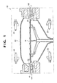
Fig. 1 is a sectional view showing an apparatus
used for annealing of the present invention;
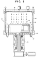
Fig. 2 is a schematic sectional view of an
apparatus described in another embodiment of the
present invention;
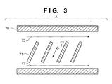
Fig. 3 is a schematic sectional view of an
apparatus described in still another embodiment of the
present invention;
Fig. 4 is a schematic sectional view of an
apparatus described in still another embodiment of the
present invention;
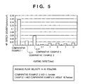
Fig. 5 is a graph showing HF defect densities
before annealing of the present invention (Comparative
Example 1), after annealing of a prior art in a
reducing atmosphere (Comparative Examples 3 and 5), and
after annealing of the present invention (Example 1);
Fig. 6 is a schematic view showing an apparatus
used in the prior art and Comparative Examples 3, 4,
and 5 of the embodiment;
Fig. 7 is a schematic view showing the flows of
an atmospheric gas in an annealing furnace shown in
Fig. 6;
Fig. 8 is a schematic sectional view for
explaining an epitaxial layer transfer method;
Fig. 9 is a graph showing the relationship
between the SOI layer thickness and HF defects in an
SOI substrate manufactured by the epitaxial layer
transfer method; and
Fig. 10 is a view showing a
scanning-electronic-microscopic image of an HF defect
center.
DETAILED DESCRIPTION OF THE PREFERRED EMBODIMENT
The embodiments of the present invention will be
described with reference to the accompanying drawings.
Fig. 1 shows an annealing apparatus suitable to
practice the present invention.
An annealing apparatus 10 shown in Fig. 1 is a
single-wafer-treating apparatus for processing SOI
wafers (not shown) one by one. The annealing apparatus
10 has a process chamber 12 formed from silica glass
and a susceptor 14 arranged in the process chamber 12
to support a wafer. A supply section 16 for supplying
a reducing gas such as hydrogen gas is formed in the
side portion of the process chamber 12. An exhaust
section 18 is formed at an opposing position. Note
that the gas supply section 16 and gas exhaust section
18 have a gas supply port 50 and gas exhaust port 51,
respectively.
A plurality of halogen lamps 20 are radially laid
out in the upper and lower regions of the process
chamber 12. In the annealing apparatus 10 using the
halogen lamps 20 with the above arrangement, an SOI
substrate is placed on the susceptor 14, and then, the
halogen lamps 20 are turned on to heat the SOI
substrate. Simultaneously, an atmospheric gas such as
hydrogen gas is supplied from the supply port 50 while
exhausting the gas from the exhaust port 18. The
atmospheric gas flows as a laminar flow along the
surface of the SOI substrate heated to a predetermined
temperature so that annealing is executed.
At this time, since the susceptor 14 rotates, the
SOI substrate can be annealed while being rotated.
After the end of annealing, the SOI substrate is
cooled to a predetermined unload temperature and
removed from the susceptor 14, thus ending the
annealing.
The annealing of the present invention is
executed at a temperature equal to or less than the
melting point of silicon. Although the lower limit of
the annealing temperature is not particularly limited,
the annealing is preferably executed at a temperature
from 800°C to 1,200°C on the basis of the results
obtained by evaluating the annealing temperature and
progress in surface planarization by movement of
surface silicon atoms in SOI substrate annealing in a
hydrogen atmosphere, which is proposed in Japanese
Patent Laid-Open No. 05-217821.
In the present invention, the annealing time is
determined by the state of an object to be processed or
the degree of a desired effect and is not particularly
defined.
In the above arrangement, since the process
chamber 12 formed from silica glass rarely absorbs
light emitted from the halogen lamps 20, the
temperature is suppressed to about 600°C or less.
Hence, H2O production by reaction between H2 and the
silica of the process chamber 12 can be prevented.
The process chamber 12 may be air-cooled by
injecting air to the process chamber 12.
Even if H2O is produced from the process chamber
12, the H2O produced from the process chamber 12 does
not reach the surface of the SOI wafer because the
atmospheric gas supplied from the supply port 16 flows
as a laminar flow along the surface of the SOI wafer.
That is, the gas flow on the wafer surface prevents H2O
produced on the chamber surface from sticking to the
wafer surface.
The apparatus used for the annealing is not
limited to the above-described lamp heating scheme.
The same effect as described above can also be obtained
by using, e.g., an apparatus of an induction heating
scheme. In this case, a silicon substrate is heated by
an eddy current flowing through the substrate because
it is a semiconductor. However, the silica of the
reactor member is not heated because it is an insulator.
The flow velocity of the gas supplied from the
gas supply port 50 is preferably 0.01 to 500 cm/s and,
more preferably, 0.1 to 100 cm/s.
The distance between the gas supply port 50 and
the edge portion of the SOI wafer opposing the gas
supply port 50 is 5 cm or less, and preferably, 1 cm or
less. The gas supply port 50 and the edge portion are
preferably actually in contact with each other.
The gas supply port 50 and the edge portion of
the SOI wafer preferably have the following positional
relationship. Preferably, the SOI surface is located
between the lowest portion of the section of the gas
pipe of the gas supply port 50 and the central axis of
the gas pipe, or the level of the lowest portion
matches the SOI wafer surface level. This is because
if a large amount of gas collides with the side surface
of the SOI wafer, the laminar gas flow is disturbed.
The diameter of the gas supply port 50 is preferably
twice or more of the SOI wafer thickness and, more
preferably, five times or more of the SOI wafer
thickness.
In annealing the SOI wafer while rotating it, the
SOI wafer can be continuously or intermittently rotated.
To intermittently rotate the SOI wafer, it can be
rotated through a predetermined angle every time a
predetermined time elapses. For example, after the
elapse of a predetermined time, the SOI wafer is
rotated clockwise through 90°, and after another elapse
of the predetermined time, the SOI wafer is rotated
counterclockwise through 180°, thereby continuing
annealing for a predetermined time. The SOI wafer may
be intermittently rotated in the same direction.
As shown in Fig. 1, the atmospheric gas can be
prevented from flowing to the lower surface of the SOI
wafer (a surface on the opposite side of the surface
where the SOI layer is present), i.e., the lower
surface can be prevented from coming into contact with
the atmospheric gas.
The SOI layer to be annealed need not always be a
single-crystal silicon layer but can be a semiconductor
layer formed from Ge, SiGe, SiC, C, GaAs, GaN, AlGaAs,
InGaAs, InP, or InAs, or a semiconductor layer
containing a plurality of types of layers selected from
them. As a semiconductor layer formed from a plurality
of types of layers, for example, a semiconductor layer
having an Si layer formed on an SiGe layer or an Si
layer formed on an SiGe layer can be used. The
semiconductor layer may be formed from a plurality of
semiconductor layers having the same composition but
different impurity concentrations or different
resistivity values (e.g., a semiconductor layer having
a two-layered structure including a silicon layer
having the first resistivity value and a silicon layer
formed on that silicon layer and having the second
resistivity value different from the first resistivity
value).
As a gas species used in annealing of the present
invention, hydrogen gas or a gas mixture containing
hydrogen gas and an inert gas (e.g., argon gas) can be
used. Any other gas species can be used as long as an
SOI layer can be planarized.
Some silicon wafers have a portion called a notch
as a mark that indicates a plane orientation or the
like. When an SOI substrate manufactured using a
silicon wafer as a material has a notch, the SOI
substrate is preferably set without directing that
portion to the gas supply port 50 and annealed.
As another embodiment, annealing can be practiced
using an epitaxial growing apparatus reported by Mitani
(Shinichi Mitani, Toshiba Technical Report No. 20,
p. 28 (1998)).
An annealing method of the present invention
using the apparatus of the above report will be
described below. The apparatus of the above report is
an epitaxial growing apparatus. In the present
invention, this apparatus is used as an annealing
apparatus in a reducing atmosphere.
An annealing apparatus 40 shown in Fig. 2 is a
single-wafer-treating apparatus for processing SOI
wafers (not shown) one by one. A process module for
processing a substrate is sealed by a stainless steel
chamber 41 having a cylindrical water cooling jacket,
and the inner surface of the chamber 41 is covered with
a liner 42 made of silica.
A holder 43 for holding a substrate and a heater
44 as a heating source are installed in the chamber.
A rotary drive mechanism 45 for rotating the
substrate and holder and the feed port for the heater
44 are arranged under the chamber.
Hydrogen gas is supplied from the upper side of
the chamber through a straightening plate 46 and
exhausted from an exhaust port 47 on the lower side.
In this apparatus, since a substrate is rotated
at a high speed of thousand-odd hundred rpm or more,
hydrogen gas supplied from the upper side of the
chamber is forcibly attracted to the wafer surface by
the pump effect of the substrate and the rotary disk of
the holder, which rotate at a high speed.
When an optimum rotational speed is selected in
accordance with the flow rate and pressure of the gas
to be supplied to the process module, hydrogen gas near
the SOI substrate surface flows as a laminar flow along
that surface.
In addition, if an optimum rotational speed is
selected in accordance with the flow rate and pressure
of the gas to be supplied to the process module, the
flow velocity of hydrogen gas near the SOI substrate
surface can be made higher than the average flow
velocity when the gas is supplied from the upper side
of the chamber through the straightening plate 46.
The embodiments of the present invention have
been described above. The present invention is not
limited to the above apparatuses, and any other
annealing apparatus capable of realizing the idea of
the present invention can be used.
For example, even a multi-wafer-treating vertical
annealing furnace as shown in Fig. 4 can obtain the
same effect as that of the present invention.
Referring to Fig. 4, reference numeral 80 denotes
a furnace tube; 81, SOI substrates; 82, atmospheric gas
supply ports; and 83, an atmospheric gas flow near the
SOI substrate surface.
As shown in Fig. 4, when one atmospheric gas
supply port 82 is arranged on each SOI substrate 81,
the atmospheric gas flow 83 parallel to the SOI
substrate surface can be generated near this surface.
Even a multi-wafer-treating vertical annealing
furnace as shown in Fig. 6 can obtain the same effect
as that of the present invention when a flow velocity
115 of an atmospheric gas near the SOI substrate
surface during annealing is prevented from
substantially becoming zero by, e.g., making a boat 105
and furnace tube have different intervals 116 and 117
therebetween.
Even a multi-wafer-treating apparatus having a
structure shown in Fig. 3 can also obtain the same
effect as that of the present invention. Referring to
Fig. 3, reference numeral 70 denotes a furnace tube; 71,
SOI substrates; and 72 and 73, atmospheric gas flows.
As shown in Fig. 3, when the SOI substrates 71
are tilted with respect to the atmospheric gas flow 72
in the reactor, and in this state, the atmospheric gas
flow 73 parallel to the SOI substrate surfaces are
generated, the effect of the present invention can be
obtained.
[Examples]
Detailed examples of the present invention will
be described below.
(SOI Substrate Manufacturing Method)
1) A CZ 6-inch (100) p+-type silicon wafer doped
with boron as a p-type impurity and having a
resistivity of 0.015 Ω·cm +/- 0.01 Ω·cm was prepared.
2) In a solution obtained by mixing 49% HF
solution and ethyl alcohol at a ratio of 2 : 1, the
silicon wafer and a 6"-diameter platinum plate were set
opposite to each other such that the silicon wafer
served as an anode and the platinum plate served as a
cathode. The lower surface side of the silicon wafer
was made to oppose the upper surface side of another
p+-type silicon wafer via the same solution. The end
wafer opposed a 6"-diameter platinum plate. The
solution was partitioned by the wafers to prevent
electrical connection between the solution parts
between the wafers. A current with a current density
of 10 mA/cm2 was supplied for 12 min to flow between
the silicon wafers and the platinum plates so as to
anodize the silicon wafers, thereby forming a plurality
of 12-µm thick porous silicon layers on the surfaces.
3) The wafers having the porous silicon layers
were oxidized in an oxygen atmosphere at 400°C. With
this oxidation processing, an only 50-Å thick oxide
film is formed. Hence, the oxide silicon film is
formed only on the surface of porous silicon and on the
inner surfaces of pores. A single-crystal silicon
region remains inside.
4) The wafers were exposed to HF solution diluted
to 1.25% for about 30 sec and dipped in pure water for
10 min to remove the very thin silicon oxide films on
the surfaces of the porous layers by overflow rinse.
5) The wafers were set in a wafer carrier and
placed in the load-lock chamber of an epitaxial CVD
growing apparatus in which the load-lock chamber where
wafers in the wafer carrier were set, a transfer
chamber having a wafer transfer robot, and a process
chamber as shown in Fig. 1 are connected. The pressure
in the load-lock chamber was reduced from the
atmospheric pressure to 133 Pa (1 Torr) or less by a
dry pump. After that, N2 was supplied to set the
pressure to 1.067 x 10⁴ Pa (80 Torr). The transfer
chamber was held at 1.067 × 10⁴ Pa (80 Torr) in advance
by supplying N2. A susceptor made of carbon with a
CVD-SiC coating is installed in the process chamber to
hold a wafer. The susceptor was heated to 750°C by an
IR lamp in advance. Hydrogen gas generated by a
hydrogen generator using a hot palladium alloy was
being supplied into the process chamber through a 10-m
long stainless steel pipe with a polished inner surface.
The wafer was transferred from the load-lock
chamber to the process chamber through the transfer
chamber by the transfer robot and placed on the
susceptor.
6) The wafer transferred onto the susceptor was
heated by an IR lamp at a rate of 100°C/min and held at
950°C for 2 sec by pre-baking processing.
SiH4 was added to the carrier gas of hydrogen at
a concentration of 28 ppm, processing is executed for
200 sec, and addition of SiH4 was stopped. After that,
the temperature was reduced to 900°C. SiH2Cl2 was added
at a concentration of 0.5 mol%. After a non-porous
single-crystal silicon film was formed, the temperature
was reduced to 750°C. The wafer was unloaded to the
load-lock chamber through the transfer chamber by the
transfer robot.
7) The wafer having the epitaxially grown
non-porous single-crystal silicon was set in a vertical
furnace. The surface of the non-porous single-crystal
silicon was oxidized in a gas mixture containing water
vapor and residual oxygen, which was formed by
combusting oxygen and hydrogen, by annealing at 1,000°C
to form a silicon oxide film having a thickness of 60
nm.
8) The above wafer and the second silicon wafer
were cleaned in the cleaning line of the silicon
semiconductor process. The two wafers were gently
stacked with their first major surfaces facing each
other, and the center of the stack was pressed to
integrate the two wafers.
9) The integrated wafer set was set in the
vertical and annealed in an oxygen atmosphere at
1,100°C for 1 hr.
10) The lower surface side of the wafer having
porous silicon formed was ground by a grinder to expose
the porous silicon across the wafer surface.
11) When the exposed porous silicon layer was
dipped in a solution mixture containing HF and hydrogen
peroxide, the porous silicon was completely removed in
about 2 hr, and an interference color by the non-porous
single-crystal silicon layer and the thermal silicon
oxide film was observed across the wafer surface.
(Comparative Example 1. Annealing in a reducing
gas atmosphere was not executed; average SOI layer
thickness = 80.3 nm)
Three SOI substrates for which the average
thickness of SOI layers formed by the above-described
epitaxial layer transfer method was 80.3 nm were not
annealed in a reducing gas atmosphere but were dipped
in a 49% hydrofluoric acid for 15 min.
HF defects in these SOI substrates were observed
using an optical microscope. In Comparative Example 1,
a range with a radius of 55 mm from the substrate
center was observed.
The numbers of observed HF defects were divided
by the observation area to obtain HF defect densities.
The HF defect densities were 0.074, 0.105, and
0.295 defects/cm2, respectively, and the average
density was 0.158 defects/cm2.
(Comparative Example 2. Annealing in a reducing
gas atmosphere was not executed; average SOI layer
thickness = 120.6 nm)
Three SOI substrates for which the average
thickness of SOI layers formed by the above-described
epitaxial layer transfer method was 120.6 nm were not
annealed in a reducing gas atmosphere but were dipped
in a 49% hydrofluoric acid for 15 min.
HF defects in these SOI substrates were observed
using an optical microscope. In Comparative Example 2,
a range with a radius of 55 mm from the substrate
center was observed.
The numbers of observed HF defects were divided
by the observation area to obtain HF defect densities.
The HF defect densities were 0.031, 0.042, and 0.042
defects/cm2, respectively, and the average density was
0.039 defects/cm2.
(Comparative Example 3. Hydrogen annealing using
vertical furnace, 1,050°C for 180 min; average SOI
layer thickness = 73.6 nm)
Two SOI substrates for which the average
thickness of SOI layers formed by the above-described
epitaxial layer transfer method in the same batch as
that of Comparative Example 1 was 78.5 nm were cleaned
by a cleaning line generally used in a silicon
semiconductor device process and set in a vertical
annealing furnace shown in Fig. 6, and annealing
disclosed in Japanese Patent Laid-Open No. 05-217821
was executed.
The average thickness value of the SOI layers in
the SOI substrates before annealing was 73.6 nm due to
etching by cleaning.
Annealing was executed in accordance with the
following procedure. A furnace lid 106 was moved
downward in advance. In this state, SOI substrates 108
were set in a boat 105. The furnace lid 106 was moved
to the position shown in Fig. 6 to place the SOI
substrates 108 in the process chamber and close the
opening portion of the furnace tube. The furnace lid
106 was operated by an elevating mechanism (not shown).
The interior of the process chamber is normally
pre-heated to about 600°C. To prevent oxidation of the
SOI substrate surfaces, a nitrogen atmosphere is formed
in the process chamber.
The interior of the process chamber was replaced
with a hydrogen gas atmosphere at the atmospheric
pressure by supplying 100% hydrogen gas from a supply
pipe 102. The hydrogen gas had been purified by a
commercially available hydrogen generator which used a
palladium alloy and was connected to the apparatus
through a 7-m long stainless steel pipe with a polished
inner surface.
The interior of the process chamber was heated to
1,050°C by a heater 104, and annealing was executed for
3 hrs.
The heating rate in heating from 600°C to 1,050°C
was 0.17°C/sec.
After the elapse of 3 hrs, the temperature of the
heater 104 was reduced, and then, the atmosphere was
replaced by supplying nitrogen gas into the process
chamber. The furnace lid 106 was moved downward, and
the SOI substrates 108 were unloaded.
These SOI substrates were dipped in 49%
hydrofluoric acid for 15 min, and HF defects within the
range with a radius of 55 nm from the substrate center
were observed using an optical microscope.
The numbers of observed HF defects were divided
by the observation area to obtain HF defect densities.
The HF defect densities were 0.042 and 0.011
defects/cm2, respectively, and the average value was
0.026 defects/cm2.
The average value of the HF defect densities was
compared with the average value of the HF defect
densities of Comparative Example 1. The HF defect
density of the SOI substrates that underwent the above
annealing was 16.4% the HF defect density of
Comparative Example 1.
(Comparative Example 4. Hydrogen annealing using
vertical furnace, 1,050°C for 180 min; average SOI
layer thickness = 114.9 nm)
Three SOI substrates for which the average
thickness of SOI layers formed by the above-described
epitaxial layer transfer method in the same batch as
that of Comparative Example 2 was 120.6 nm were cleaned
by a cleaning line generally used in a silicon
semiconductor device process and annealed by the same
method as that of Comparative Example 3.
The average thickness value of the SOI layers in
the SOI substrates before annealing was 114.9 nm due to
etching by cleaning.
These SOI substrates were dipped in 49%
hydrofluoric acid for 15 min, and HF defects within the
range with a radius of 55 nm from the substrate center
were observed using an optical microscope.
The numbers of observed HF defects were divided
by the observation area to obtain HF defect densities.
The HF defect densities were 0, 0.021, and 0
defects/cm2, respectively, and the average value was
0.007 defects/cm2.
The average value of the HF defect densities was
compared with the average value of the HF defect
densities of Comparative Example 2. The HF defect
density of the SOI substrates that underwent the above
annealing was 18.4% the HF defect density of
Comparative Example 2.
(Comparative Example 5. Hydrogen annealing using
vertical furnace, 1,050°C for 3 min; average SOI layer
thickness = 74.9 nm)
Two SOI substrates for which the average
thickness of SOI layers formed by the above-described
epitaxial layer transfer method in the same batch as
that of Comparative Example 1 was 81.2 nm were cleaned
by a cleaning line generally used in a silicon
semiconductor device process and set in a vertical
hydrogen annealing furnace shown in Fig. 6, and
annealing disclosed in Japanese Patent Laid-Open
No. 05-217821 was executed.
The average thickness value of the SOI layers in
the SOI substrates before annealing was 74.9 nm due to
etching by cleaning.
Annealing was executed in accordance with the
following procedure. A furnace lid 106 was moved
downward in advance. In this state, SOI wafers 108
were set in a boat 105. The furnace lid 106 was moved
to the position shown in Fig. 6 to place the SOI wafers
108 in the process chamber and close the opening
portion of the furnace tube. The furnace lid 106 was
operated by an elevating mechanism (not shown).
The interior of the process chamber is normally
pre-heated to about 600°C.
To prevent oxidation of the SOI substrate
surfaces, a nitrogen atmosphere is formed in the
process chamber.
The interior of the process chamber was replaced
with a hydrogen gas atmosphere at the atmospheric
pressure by supplying 100% hydrogen gas from a supply
pipe 102. The hydrogen gas had been purified by a
commercially available hydrogen generator which used a
palladium alloy and was connected to the apparatus
through a 7-m long stainless steel pipe with a polished
inner surface.
The interior of the process chamber was heated to
1,050°C by a heater 104, and annealing was executed for
3 min.
The heating rate in heating from 600°C to 1,050°C
was 0.17°C/sec.
After the elapse of 3 min, the temperature of the
heater 104 was reduced, and then, the atmosphere was
replaced by supplying nitrogen gas into the process
chamber. The furnace lid 106 was moved downward, and
the SOI wafers 108 were unloaded.
These SOI substrates were dipped in 49%
hydrofluoric acid for 15 min, and HF defects within the
range with a radius of 55 nm from the substrate center
were observed using an optical microscope.
The numbers of observed HF defects were divided
by the observation area to obtain HF defect densities.
The HF defect densities were 0.032 and 0.084
defects/cm2, respectively, and the average value was
0.058 defects/cm2.
(Example 1. Processing by single-wafer-treating
epitaxial growing apparatus; average SOI layer
thickness = 74.9 nm)
Fifteen SOI substrates for which the average
thickness of SOI layers formed by the above-described
epitaxial layer transfer method in the same batch as
that of Comparative Example 1 was 79.1 nm were cleaned
by a cleaning line generally used in a silicon
semiconductor device process and annealed by a
single-wafer-treating epitaxial growing apparatus.
The average thickness value of the SOI layers in
the SOI substrates before annealing was 74.9 nm due to
etching by cleaning.
The single-wafer-treating epitaxial growing
apparatus used in Example 1 comprises a load-lock
chamber (Fig. 1) of an epitaxial CVD growing apparatus
to which a load-lock chamber where wafers in a wafer
carrier were set, a transfer chamber (not shown) with a
wafer transfer robot set, and a process chamber are
connected.
Annealing was executed in accordance with the
following procedure. First, the SOI substrates were
set in a wafer carrier and placed in the load-lock
chamber.
The pressure in the load-lock chamber was reduced
from the atmospheric pressure to 133 Pa (1 Torr) or
less by a dry pump. After that, N2 gas was supplied to
set the pressure to 1.067 x 10⁴ Pa (80 Torr). The
transfer chamber was held at 1.067 × 10⁴ Pa (80 Torr)
in advance by supplying N2. A susceptor 14 made of
carbon with a SiC coating was installed in the process
chamber to hold a wafer. The susceptor 14 was heated
to 750°C by a halogen lamp in advance. Hydrogen gas
generated by a hydrogen generator using a hot palladium
alloy was being supplied into the process chamber
through a 10-m long stainless steel pipe with a
polished inner surface.
The SOI substrate was transferred from the
load-lock chamber to the process chamber through the
transfer chamber by the transfer robot and placed on
the susceptor.
The pressure in the process chamber was set to 8
x 104 Pa (600 Torr). Then, the SOI substrate placed on
the susceptor was heated to 1,050°C by the halogen lamp
and annealed for 3 min.
The average flow velocity in the reactor was
about 46.7 cm/sec.
The heating rate in heating from 750°C to 1,050°C
(annealing temperature) was tested for 5 standards each
using three substrates (Table 1).
| Heating rate (°C/sec) | 0.1 | 1 | 5 | 7 | 10 |
| Number of processed substrates | 3 | 3 | 3 | 3 | 3 |
After annealing, the temperature was reduced to
750°C. The SOI substrate was unloaded to the load-lock
chamber through the transfer chamber by the transfer
robot.
These SOI substrates were dipped in 49%
hydrofluoric acid for 15 min, and HF defects within the
range with a radius of 55 nm from the substrate center
were observed using an optical microscope.
The numbers of observed HF defects were divided
by the observation area to obtain HF defect densities.
The average value of the HF defect densities of the 15
annealed substrates was 0.008 defects/cm2.
The average value of the HF defect densities was
compared with the average value of the HF defect
densities of Comparative Example 1. The HF defect
density of the SOI substrates that underwent the above
annealing was 5.1% the HF defect density of Comparative
Example 1.
It was confirmed that the number of HF defects
decreased by annealing of Example 1.
The average value of the HF defect densities was
compared with the average value of the HF defect
densities of Comparative Example 3. The HF defect
density of the SOI substrates that underwent the above
annealing was 30.8% the HF defect density of
Comparative Example 3.
As is apparent from this result, the HF defect
reduction effect by annealing of the present invention
is higher than annealing in a reducing atmosphere using
a vertical annealing furnace disclosed in Japanese
Patent Laid-Open No. 05-217821.
Table 2 shows the relationship between the HF
defect density and the heating rate from 750°C to
1,050°C (annealing temperature).
| Heating rate (°C/sec) | 0.1 | 1 | 5 | 7 | 10 |
| Average thickness of SOI layer (nm) | 74.5 | 74.7 | 75.9 | 74.6 | 74.7 |
| HF defect density average value (defects/cm2) | 0.004 | 0.011 | 0.011 | 0.007 | 0.011 |
As shown in Table 2, no correlation was observed
between the HF defect density and the heating rate to
the annealing temperature.
To obtain a finding about the correlation between
the annealing time and the HF defect density, the
result of HF defect densities of Example 1 was compared
with the average value of the HF defect densities of
Comparative Example 5.
In Comparative Example 5, annealing in a reducing
atmosphere using a vertical annealing furnace was
executed, and the annealing time was set to 3 min as in
Example 1.
The heating rate to the annealing temperature was
0.17°C/sec.
The average value of HF defect densities of
Comparative Example 5 is 0.058 defects/cm2. This is
larger than the HF defect density average value of
Example 1 at the closest heating rate of 0.1°C/sec by
14.5 times.
Hence, the annealing time and the HF defect
density reduction effect have no correlation.
As is apparent from the above result, the HF
defect reduction effect of Example 1 derives from the
flow velocity of the atmospheric gas near the SOI
substrate surface parallel to the SOI substrate surface
in annealing.
(Comparative Example 6. Processing by
single-wafer-treating epitaxial growing apparatus;
average SOI layer thickness = 114.3 nm)
Fifteen SOI substrates for which the average
thickness of SOI layers formed by the above-described
epitaxial layer transfer method in the same batch as
that of Comparative Example 2 was 119.1 nm were cleaned
by a cleaning line generally used in a silicon
semiconductor device process and annealed by the same
method as that of Example 1.
The average thickness value of the SOI layers in
the SOI substrates before annealing was 114.3 nm due to
etching by cleaning.
The heating rate in heating from 750°C to 1,050°C
(annealing temperature) was tested for 5 standards each
using three substrates (Table 1).
After annealing, these SOI substrates were dipped
in 49% hydrofluoric acid for 15 min, and HF defects
within the range with a radius of 55 nm from the
substrate center were observed using an optical
microscope.
The numbers of observed HF defects were divided
by the observation area to obtain HF defect densities.
The average value of the HF defect densities of the 15
annealed substrates was 0.009 defects/cm2.
The average value of the HF defect densities was
compared with the average value of the HF defect
densities of Comparative Example 2. The HF defect
density of the SOI substrates that underwent the above
annealing was 23.7% the HF defect density of
Comparative Example 2.
It was confirmed that HF defects was decreased by
annealing with the reducing atmosphere.
The average value (0.009 defects/cm2) of the HF
defect densities was compared with the average value of
the HF defect densities of Comparative Example 4. The
HF defect density of the SOI substrates that underwent
the above annealing was 1.29 times that of Comparative
Example 4. That is, there were not remarkable
differences between Comparative Example 6 and
Comparative Example 4. The differences between
Comparative Example 3 and Example 1, and the
differences between Comparative Example 4 and
Comparative Example 6 indicate that when the thickness
of SOI layer is thin enough, e.g., the thickness is 100
nm or less, the effect of the present invention becomes
large.
Table 3 shows the relationship between the HF
defect density and the heating rate from 750°C to
1,050°C (annealing temperature) in Comparative Example
6.
| Heating rate (°C/sec) | 0.1 | 1 | 5 | 7 | 10 |
| Average thickness of SOI layer (nm) | 114.8 | 114.4 | 112.3 | 114.6 | 115.1 |
| HF defect density average value (defects/cm2) | 0.028 | 0.003 | 0 | 0.007 | 0.007 |
As shown in Table 3, no correlation was observed
between the HF defect density and the heating rate to
the annealing temperature.
Fig. 5 is a graph showing HF defect density
average values before annealing of the present
invention (Comparative Example 1), after the
conventional annealing in a reducing atmosphere
(Comparative Examples 3 and 5), and after annealing of
the present invention (Example 1). According to the
present invention, defects (HF defects) in the SOI
layer of an SOI substrate and, more particularly, HF
defects that increase as the SOI layer becomes thin can
be reduced by annealing the SOI substrate in a reducing
gas atmosphere.
As has been described above, according to the
present invention, defects (HF defects) in the SOI
layer of an SOI substrate and, more particularly, HF
defects that increase as the SOI layer becomes thin can
be reduced by annealing the SOI substrate in a reducing
gas atmosphere.
Hence, a high-quality thin film SOI substrate
with minimum HF defects can be provided.
As many apparently widely different embodiments of
the present invention can be made without departing from
the spirit and scope thereof, it is to be understood
that the invention is not limited to the specific
embodiments thereof except as defined in the appended
claims.
The number of defects (HF defects) in the SOI
layer of an SOI substrate is reduced. In an annealing
method of annealing an SOI substrate in a reducing
atmosphere at a temperature equal to or less than the
melting point of a semiconductor, annealing is executed
in a state wherein a flow of a reducing atmospheric gas
parallel to the surface of the SOI substrate is
generated near this surface.