EP1193537A1 - Optical waveguide - Google Patents
Optical waveguide Download PDFInfo
- Publication number
- EP1193537A1 EP1193537A1 EP01908311A EP01908311A EP1193537A1 EP 1193537 A1 EP1193537 A1 EP 1193537A1 EP 01908311 A EP01908311 A EP 01908311A EP 01908311 A EP01908311 A EP 01908311A EP 1193537 A1 EP1193537 A1 EP 1193537A1
- Authority
- EP
- European Patent Office
- Prior art keywords
- optical waveguide
- electrode
- signal electrode
- branched
- ground
- Prior art date
- Legal status (The legal status is an assumption and is not a legal conclusion. Google has not performed a legal analysis and makes no representation as to the accuracy of the status listed.)
- Granted
Links
- 230000003287 optical effect Effects 0.000 title claims abstract description 300
- 239000000758 substrate Substances 0.000 claims abstract description 40
- 239000010409 thin film Substances 0.000 claims description 14
- 239000000463 material Substances 0.000 claims description 13
- 230000005693 optoelectronics Effects 0.000 claims description 12
- 239000004020 conductor Substances 0.000 claims description 4
- 239000013307 optical fiber Substances 0.000 description 18
- 239000013078 crystal Substances 0.000 description 10
- 230000005540 biological transmission Effects 0.000 description 9
- 238000000034 method Methods 0.000 description 7
- 239000010936 titanium Substances 0.000 description 6
- 238000004891 communication Methods 0.000 description 5
- 230000007613 environmental effect Effects 0.000 description 5
- 230000000052 comparative effect Effects 0.000 description 3
- XEEYBQQBJWHFJM-UHFFFAOYSA-N Iron Chemical compound [Fe] XEEYBQQBJWHFJM-UHFFFAOYSA-N 0.000 description 2
- RTAQQCXQSZGOHL-UHFFFAOYSA-N Titanium Chemical compound [Ti] RTAQQCXQSZGOHL-UHFFFAOYSA-N 0.000 description 2
- 229910052802 copper Inorganic materials 0.000 description 2
- 230000003247 decreasing effect Effects 0.000 description 2
- 238000000151 deposition Methods 0.000 description 2
- 230000006866 deterioration Effects 0.000 description 2
- 238000009792 diffusion process Methods 0.000 description 2
- 230000005684 electric field Effects 0.000 description 2
- 229910052737 gold Inorganic materials 0.000 description 2
- GQYHUHYESMUTHG-UHFFFAOYSA-N lithium niobate Chemical compound [Li+].[O-][Nb](=O)=O GQYHUHYESMUTHG-UHFFFAOYSA-N 0.000 description 2
- 238000007747 plating Methods 0.000 description 2
- 238000004544 sputter deposition Methods 0.000 description 2
- 229910052719 titanium Inorganic materials 0.000 description 2
- WSMQKESQZFQMFW-UHFFFAOYSA-N 5-methyl-pyrazole-3-carboxylic acid Chemical compound CC1=CC(C(O)=O)=NN1 WSMQKESQZFQMFW-UHFFFAOYSA-N 0.000 description 1
- 229910003327 LiNbO3 Inorganic materials 0.000 description 1
- 229910018487 Ni—Cr Inorganic materials 0.000 description 1
- VYPSYNLAJGMNEJ-UHFFFAOYSA-N Silicium dioxide Chemical compound O=[Si]=O VYPSYNLAJGMNEJ-UHFFFAOYSA-N 0.000 description 1
- 230000015572 biosynthetic process Effects 0.000 description 1
- 230000015556 catabolic process Effects 0.000 description 1
- 238000006731 degradation reaction Methods 0.000 description 1
- 230000008021 deposition Effects 0.000 description 1
- 239000006185 dispersion Substances 0.000 description 1
- 239000000835 fiber Substances 0.000 description 1
- 229910052742 iron Inorganic materials 0.000 description 1
- 229910052746 lanthanum Inorganic materials 0.000 description 1
- FZLIPJUXYLNCLC-UHFFFAOYSA-N lanthanum atom Chemical compound [La] FZLIPJUXYLNCLC-UHFFFAOYSA-N 0.000 description 1
- 230000007774 longterm Effects 0.000 description 1
- 238000012986 modification Methods 0.000 description 1
- 230000004048 modification Effects 0.000 description 1
- 229920002120 photoresistant polymer Polymers 0.000 description 1
- 229910052814 silicon oxide Inorganic materials 0.000 description 1
- 229910052709 silver Inorganic materials 0.000 description 1
- 230000005477 standard model Effects 0.000 description 1
- 238000001771 vacuum deposition Methods 0.000 description 1
Images



Classifications
-
- G—PHYSICS
- G02—OPTICS
- G02F—OPTICAL DEVICES OR ARRANGEMENTS FOR THE CONTROL OF LIGHT BY MODIFICATION OF THE OPTICAL PROPERTIES OF THE MEDIA OF THE ELEMENTS INVOLVED THEREIN; NON-LINEAR OPTICS; FREQUENCY-CHANGING OF LIGHT; OPTICAL LOGIC ELEMENTS; OPTICAL ANALOGUE/DIGITAL CONVERTERS
- G02F1/00—Devices or arrangements for the control of the intensity, colour, phase, polarisation or direction of light arriving from an independent light source, e.g. switching, gating or modulating; Non-linear optics
- G02F1/01—Devices or arrangements for the control of the intensity, colour, phase, polarisation or direction of light arriving from an independent light source, e.g. switching, gating or modulating; Non-linear optics for the control of the intensity, phase, polarisation or colour
- G02F1/21—Devices or arrangements for the control of the intensity, colour, phase, polarisation or direction of light arriving from an independent light source, e.g. switching, gating or modulating; Non-linear optics for the control of the intensity, phase, polarisation or colour by interference
- G02F1/225—Devices or arrangements for the control of the intensity, colour, phase, polarisation or direction of light arriving from an independent light source, e.g. switching, gating or modulating; Non-linear optics for the control of the intensity, phase, polarisation or colour by interference in an optical waveguide structure
- G02F1/2255—Devices or arrangements for the control of the intensity, colour, phase, polarisation or direction of light arriving from an independent light source, e.g. switching, gating or modulating; Non-linear optics for the control of the intensity, phase, polarisation or colour by interference in an optical waveguide structure controlled by a high-frequency electromagnetic component in an electric waveguide structure
-
- G—PHYSICS
- G02—OPTICS
- G02F—OPTICAL DEVICES OR ARRANGEMENTS FOR THE CONTROL OF LIGHT BY MODIFICATION OF THE OPTICAL PROPERTIES OF THE MEDIA OF THE ELEMENTS INVOLVED THEREIN; NON-LINEAR OPTICS; FREQUENCY-CHANGING OF LIGHT; OPTICAL LOGIC ELEMENTS; OPTICAL ANALOGUE/DIGITAL CONVERTERS
- G02F1/00—Devices or arrangements for the control of the intensity, colour, phase, polarisation or direction of light arriving from an independent light source, e.g. switching, gating or modulating; Non-linear optics
- G02F1/01—Devices or arrangements for the control of the intensity, colour, phase, polarisation or direction of light arriving from an independent light source, e.g. switching, gating or modulating; Non-linear optics for the control of the intensity, phase, polarisation or colour
- G02F1/03—Devices or arrangements for the control of the intensity, colour, phase, polarisation or direction of light arriving from an independent light source, e.g. switching, gating or modulating; Non-linear optics for the control of the intensity, phase, polarisation or colour based on ceramics or electro-optical crystals, e.g. exhibiting Pockels effect or Kerr effect
- G02F1/0305—Constructional arrangements
- G02F1/0316—Electrodes
-
- G—PHYSICS
- G02—OPTICS
- G02F—OPTICAL DEVICES OR ARRANGEMENTS FOR THE CONTROL OF LIGHT BY MODIFICATION OF THE OPTICAL PROPERTIES OF THE MEDIA OF THE ELEMENTS INVOLVED THEREIN; NON-LINEAR OPTICS; FREQUENCY-CHANGING OF LIGHT; OPTICAL LOGIC ELEMENTS; OPTICAL ANALOGUE/DIGITAL CONVERTERS
- G02F1/00—Devices or arrangements for the control of the intensity, colour, phase, polarisation or direction of light arriving from an independent light source, e.g. switching, gating or modulating; Non-linear optics
- G02F1/01—Devices or arrangements for the control of the intensity, colour, phase, polarisation or direction of light arriving from an independent light source, e.g. switching, gating or modulating; Non-linear optics for the control of the intensity, phase, polarisation or colour
- G02F1/21—Devices or arrangements for the control of the intensity, colour, phase, polarisation or direction of light arriving from an independent light source, e.g. switching, gating or modulating; Non-linear optics for the control of the intensity, phase, polarisation or colour by interference
- G02F1/225—Devices or arrangements for the control of the intensity, colour, phase, polarisation or direction of light arriving from an independent light source, e.g. switching, gating or modulating; Non-linear optics for the control of the intensity, phase, polarisation or colour by interference in an optical waveguide structure
Definitions
- This invention relates to an optical waveguide element, particularly to an optical waveguide element suitable for a high velocity optical modulator in high velocity and large capacity optical fiber communication system.
- Such an optical waveguide modulator is constructed as follows.
- Fig. 1 is a cross sectional view schematically showing an optical waveguide element used in a conventional high velocity modulator.
- Fig. 2 is a cross sectional view schematically showing another optical waveguide element used in a conventional high velocity modulator.
- An optical waveguide element 10 depicted in Fig. 1 includes a substrate 1 made of a Z-cut single crystal of electro-optical effect and a buffer layer 2 formed on the substrate 1. Moreover, the optical modulator 10 has a first and a second branched optical waveguides 3-1 and 3-2 in the substrate 1, formed by a titanium inter-diffusion method or the like. The optical waveguides 3-1 and 3-2 are made a pair to construct a Mach-Zehnder type optical waveguide.
- a signal electrode to apply a modulating signal to an optical wave through the first branched optical waveguide 3-1, and ground electrodes 5-1 and 5-2.
- the signal electrode 4 is disposed directly on the first optical waveguide 3-1.
- the ground electrodes 5-1 and 5-2 serve as opposed electrodes for the signal electrode 4, and are disposed as near as possible the signal electrode 4 so that the total impedance of the electrodes is matched to 50 ⁇ of external impedance and the driving voltage is reduced.
- An optical waveguide element 20 depicted in Fig. 2 includes a substrate 11 made of a X-cut single crystal of electro-optical effect and a buffer layer 12 formed on the substrate 11. Moreover, similar to the optical waveguide element 10, the optical waveguide element 20 has a first and a second branched optical waveguides 13-1 and 13-2 to construct a Mach-Zehnder type optical waveguide. Moreover, on the buffer layer 12, are provided signal electrode 14 and ground electrodes 15-1 and 15-2.
- the branched optical waveguide 13-2 is disposed directly under the ground electrode 15-2 so as to apply chirp to an optical wave through the waveguide 13-2.
- the ground electrodes 15-1 and 15-2 serves as opposed electrodes for the signal electrode as mentioned above.
- a given half-wavelength voltage is applied to the signal electrodes 4 and 14, to shift the phases of optical waves through the first branched optical waveguides 3-1 and 13-1 for the phases of optical waves through the second branched optical waveguide 3-2 and 13-2 by ⁇ , and thus, to switch on/off an optical signal superimposed on an optical waveguide.
- the half-wavelength voltage is calculated on a voltage magnitude when the phase of the optical wave is shifted by ⁇ from a standard operation point, which is pre-determined on the optical intensity modulation curve of the optical waveguide element.
- the operation point may be shifted due to the change of environmental temperature. Therefore, the half-wavelength voltage is shifted from the pre-determined value, and thus, the optical waveguide element can not be switched on/off well.
- the high reliability and the high stability of the fiber communication system can not be satisfied.
- this invention relates to an optical waveguide element (first optical waveguide element) including a substrate made of a material with electro-optical effect, a Mach-Zehnder type optical waveguide formed at the main surface of the substrate, and a modulating electrode to control an optical wave through the Mach-Zehnder type optical waveguide.
- the Mach-Zehnder type optical waveguide includes a first branched optical waveguide and a second branched optical waveguide
- the modulating electrode includes a signal electrode to modulate an optical wave through the first branched optical waveguide of the Mach-Zehnder type optical waveguide and a ground electrode serving as an opposed electrode for the signal electrode.
- the ground electrode is composed of a first ground electrode and a second ground electrode which are opposed each other with sandwiching the signal electrode.
- the first branched optical waveguide is disposed under the signal electrode or in between the first ground electrode and the signal electrode, and the second branched optical electrode is disposed under the second ground electrode.
- the second ground electrode is partially cut away along the long direction and divided, to substantially symmetrize the modulating electrode composed of the signal electrode, the first and the second ground electrodes on the center line between the first and the second branched optical waveguides. Then, the ratio (d2/d1) of the distance d2 between the signal electrode and the second branched optical waveguide to the distance d1 between the signal electrode and the first branched optical waveguide is set within 3.5-7.5.
- This invention also relates to an optical waveguide element (second optical waveguide element) including a substrate made of a material with electro-optical effect, a Mach-Zehnder type optical waveguide formed at the main surface of the substrate, and a modulating electrode to control an optical wave through the Mach-Zehnder type optical waveguide.
- the Mach-Zehnder type optical waveguide includes a first branched optical waveguide and a second branched optical waveguide
- the modulating electrode includes a signal electrode to modulate an optical wave through the first branched optical waveguide of the Mach-Zehnder type optical waveguide and a ground electrode serving as an opposed electrode for the signal electrode.
- the ground electrode is composed of a first ground electrode and a second ground electrode which are opposed each other with sandwiching the signal electrode.
- the first branched optical waveguide is disposed under the signal electrode or in between the first ground electrode and the signal electrode, and the second branched optical electrode is disposed under the second ground electrode.
- the second ground electrode is partially cut away along the long direction and divided, to substantially symmetrize the modulating electrode composed of the signal electrode, the first and the second ground electrodes on the center line between the first and the second branched optical waveguides. Then, the ratio (Ws/Wg) of the width Ws of the signal electrode to the width Wg of the divided part of the second ground electrode located near the signal electrode is set within 0.5-4.
- this invention relates to an optical waveguide element (third optical waveguide element) including a substrate made of a material with electro-optical effect, a Mach-Zehnder type optical waveguide formed at the main surface of the substrate, and a modulating electrode to control an optical wave through the Mach-Zehnder type optical waveguide.
- the Mach-Zehnder type optical waveguide includes a first branched optical waveguide and a second branched optical waveguide
- the modulating electrode includes a signal electrode to modulate an optical wave through the first branched optical waveguide of the Mach-Zehnder type optical waveguide and a ground electrode serving as an opposed electrode for the signal electrode.
- the ground electrode is composed of a first ground electrode and a second ground electrode which are opposed each other with sandwiching the signal electrode.
- the first branched optical waveguide is disposed under the signal electrode or in between the first ground electrode and the signal electrode, and the second branched optical electrode is disposed under the second ground electrode.
- the second ground electrode is partially cut away along the long direction and divided into three parts, and the divided first part is disposed on the almost center line between the first and the second branched optical waveguides, and the divided second part and the divided third part are almost the same as the signal electrode and the first ground electrode in figuration and dimension, respectively, to substantially symmetrize the modulating electrode composed of the signal electrode, the first and the second ground electrodes on the center line between the first and the second branched optical waveguides. Then, the width W1 of the divided first part is set 0.5-20 times as large as the width Ws of the signal electrode.
- the inventors had intensely studied to find out the cause of operation point shift as mentioned above. Then, they paid attention to "DC drift” and "temperature drift” which are estimated to be two kinds of main factor for the operation point drift, and investigated the operation point shift precisely on the main factors.
- the inventors had precisely investigated the operation point shift on the temperature drift, and paid attention to the configuration differences of the optical waveguide elements 10 and 20 around the first branched optical waveguides 3-1 and 13-1 and the second branched optical waveguides 3-2 and 13-2.
- the inventors found out that the operation point shift is caused remarkably when the figurations and the dimensions of the signal electrodes 4 and 14 and the ground electrodes 5-1, 5-2, 15-1 and 15-2 are changed. That is, if the figurations and the dimensions of the signal electrodes and the ground electrodes are different, different stresses are exerted on the substrate from the electrodes as the environmental temperature is increased. Accordingly, the refractive index around the optical waveguide is changed due to the different stresses, and the optical waveguide suffers from the refractive index change to cause the operation point shift.
- the optical waveguide element 10 shown in Fig. 1 for example, since the figurations and the dimensions of the signal electrode 4 and the ground electrodes 5-1 and 5-2, which are called as a "modulating electrode", are different one another, different stresses are exerted on the substrate 1 from the electrodes, respectively as the environmental temperature is increased. Therefore, the refractive index change around the signal electrode 4 is different from the ones around the ground electrodes 5-1 and 5-2, and thus, the optical waveguides 3-1 and 3-2 suffer from the respective different refractive index changes from the electrodes. Accordingly, in the optical waveguide element 10, the operation point shift is caused due to the temperature drift.
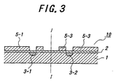
- the inventors have fabricated the portion corresponding to the distance W0 between the ground electrode 5-1 and the signal electrode 4 at the ground electrode 5-2 in Fig. 1, to substantially symmetrize the ground electrode 5-1 and the signal electrode 4 for the ground electrode 5-2 on the center line I-I between the branched optical waveguides 3-1 and 3-2. That is, the ground electrode 5-2 is partially cut away by a W0 width along the long direction of the branched optical waveguides 3-1 and 3-2, to be divided, as shown in Fig. 3. The thus obtained ground electrode 5-3 is symmetrized for the signal electrode 4 and the ground electrode 5-1 on the center line I-I in configuration.
- the figuration and the dimension of the electrodes are symmetrized on both sides from the center line I-I, so the almost same stress is exerted on the substrate from each of the electrodes and thus, the almost same refractive index change is created around the branched optical waveguides 3-1 and 3-2 as the environmental temperature is increased. As a result, the temperature drift is repressed effectively, and thus, the operation point shift can be prevented.
- the inventors had also intensely studied to iron out the deterioration of the transmission property. As a result, they found out that the deterioration of the transmission property results from the chirp characteristic of the optical waveguide element. Conventionally, it was assumed that as the magnitude of the chirp of the optical waveguide element is decreased, the optical fiber dispersion is decreased, to develop the transmission property of the optical fiber. However, the inventors found out that the transmission property of the optical fiber may be developed if the chirp of the optical waveguide element is set to be a larger value, depending the kind and the length of the optical fiber to be used, and the preferable chirp value is within about 0.4-1.0, particularly within about 0.6-0.8.
- the inventors made an attempt to control the chirp of such an optical waveguide element as shown in Fig. 3 in which the operation point shift can be prevented.
- the ratio of the distance between the signal electrode and the first branched optical waveguide to the distance between the signal electrode and the second branched optical waveguide is set to a given value, and thus, the stress exerted on around the first branched optical waveguide and the stress exerted on around the second branched optical waveguide are balanced and substantially symmetrized in both sides from the center between the branched optical waveguides, the chirp characteristic of the optical waveguide element can be controlled with preventing the operation point shift.
- the first optical waveguide element of the present invention is realized on the above-mentioned fact of the matter.
- Fig. 4 is a cross sectional view showing one example of the first optical waveguide element of the present invention.
- the dimensions and figurations of some parts are different from the real ones.
- An optical waveguide element 30 includes a substrate 21 made of a X-cut ferroelectric single crystal with electro-optical effect, a buffer layer 22 and a first and a second branched optical waveguides 23-1 and 23-2 to constitute a Mach-Zehnder type optical waveguide at the surface of the substrate 21. Then, on the buffer layer 22, are provided a signal electrode 24, a first ground electrode 25-1 and a second ground electrode 25-2. The second ground electrode 25-2 is partially cut away along the long direction and divided, to form a ditch 26 therein. As a result, the first ground electrode 25-1, the signal electrode 24 and the second ground electrode 25-2 are arranged symmetrically on the center line II-II between the branched optical waveguides. Therefore, the operation point shift of the optical waveguide element 30 can be prevented.
- the ratio (d2/d1) of the distance d2 between the signal electrode 24 and the second branched optical electrode 23-2 for the distance d1 between the signal electrode 24 and the first branched optical waveguide 23-1 is set within 3.5-7.5, according to the present invention.
- the overlap degree of a signal electric field to be applied are made asymmetric for the first and the second branched optical waveguides 23-1 and 23-2, with balancing the stresses from the electrodes on the center line II-II. Therefore, chirp can be created in the optical waveguide element 30 to some degree with preventing the temperature drift thereof. Concretely, chirp of about 0.6-0.8 can be created in the element 30. Therefore, in the optical waveguide element 30 according to the first optical waveguide element of the present invention, the operation point shift can be prevented, and the transmission property can be improved through the chirp creation of about 0.6-0.8.
- the inventors also found out that in such an optical waveguide element as shown in Fig. 3, if the width of the signal electrode is shifted to the width of the second ground electrode, and thus, the ratio of the width of the signal electrode to the width of the second ground electrode is set to a given value, with symmetrizing the signal electrode and the ground electrodes, the chirp characteristic of the optical waveguide element can be controlled.
- the second optical waveguide element of the present invention is realized on the fact of the matter.
- Fig. 5 is a cross sectional view showing one example of the second optical waveguide element of the present invention.
- An optical waveguide element 40 as shown in Fig. 5 includes a substrate 31 made of a X-cut ferroelectric single crystal with electro-optical effect, a buffer layer 32, and a first and a second branched optical waveguides 33-1 and 33-2 to constitute a Mach-Zehnder type optical waveguide at the surface of the substrate 31. Then, on the buffer layer 32, are provided a signal electrode 34, a first and a second ground electrodes 35-1 and 35-2. The second ground electrode 35-2 is partially cut away along the long direction, and divided.
- the first ground electrode 35-1, the signal electrode 34 and the second ground electrode 35-2 are arranged substantially symmetrically on the center line III-III between the first and the second branched optical waveguides 33-1 and 33-2. Therefore, the operation point shift can be prevented.
- the ratio (Ws/Wg) of the width Ws of the signal electrode 34 to the width Wg of the second ground electrode 35-2 is set within 0.5-4. Therefore, the overlap degree of a signal electric field to be applied are made asymmetric for the first and the second branched optical waveguides 33-1 and 33-2, with balancing the stresses from the electrodes on the center line III-III. Therefore, chirp can be created in the optical waveguide element 40 to some degree with preventing the temperature drift thereof. Concretely, chirp of about 0.4-0.9 can be created in the element 40. Therefore, in the optical waveguide element 40 according to the second optical waveguide element of the present invention, the operation point shift can be prevented, and the transmission property can be improved through the chirp creation of about 0.4-0.9.
- the inventors also contrived the configuration of the second ground electrode divided in symmetrizing the signal electrode and the ground electrodes on the center line between the branched optical waveguides.
- the second ground electrode is divided into two parts, to symmetrize the electrodes on the center line.
- the second ground electrode is divided into three parts, and the divided first part located near the signal electrode is disposed on the center line between the branched optical waveguides.
- the signal electrode and the ground electrodes are arranged substantially symmetically on the center line between the branched optical waveguides, the operation point shift can be effectively prevented.
- the width of the first part is set to a given value as compared with the width of the signal electrode, the chirp characteristic can be controlled.
- the third optical waveguide electrode is realized on the fact of the matter.
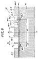
- FIG. 6 is a cross sectional view showing one example of the third optical waveguide element of the present invention.
- An optical waveguide element 50 shown in Fig. 6 includes a substrate 41 made of a X-cut ferroelectric single crystal with electro-optical effect, a buffer layer 42, and a first and a second branched optical waveguides 43-1 and 43-2 to constitute a Mach-Zehnder type optical waveguide at the surface of the substrate 41. Then, on the buffer layer 42, are provided a signal electrode 44, a first and a second ground electrodes 45-1 and 45-2.
- the second ground electrode 45-2 is partially cut away along the long direction and divided in three parts, to form ditches 46-1 and 46-2.
- the second ground electrode 45-2 is constructed of a first part 48-1, a second part 48-1 and a third part 48-3.
- the width W1 of the first part 48-1 of the second ground electrode 45-1 is set 0.5-20 time as large as the width Ws of the signal electrode 44, an asymmetric signal can be applied to the first and the second branched optical waveguides with balancing the stresses from the electrodes for the optical waveguides.
- chirp can be created in the optical waveguide element with preventing the operation point shift.
- chirp of about 0.4-1.0 can be created in the optical waveguide element. Accordingly, in the optical waveguide element 50 according to the third optical waveguide element of the present invention, the operation point shift can be prevented, and the transmission property can be improved through the chirp creation of about 0.4-1.0.
- the phrase "the second branched optical waveguide is disposed under the second ground electrode” includes the state in which the second branched optical waveguide is disposed under the not-divided second ground electrode, concretely the state in which the second branched optical waveguide is disposed under a thin film formed at the ditch of the divided second ground electrode as shown in Fig. 5.
- the ratio of the width of the signal electrode to the width of the divided part of the second ground electrode located near the signal electrode is set within the above-mentioned range, chirp of a given magnitude can be created in the optical waveguide element.
- the distance between the first branched optical waveguide and the signal electrode is set different from the distance between the second branched optical waveguide and the signal electrode. That is, in the optical waveguide element 40 shown in Fig. 5, the ratio (d2/d1) of the distance d2 between the signal electrode 34 and the second branched optical electrode 33-2 to the distance d1 between the signal electrode 34 and the first branched optical electrode 33-1 is set within 3.5-7.5, particularly 5.4-6.0.
- the distance between the first branched optical waveguide and the signal electrode is set different from the distance between the second branched optical waveguide and the signal electrode, as mentioned above. That is, in the optical waveguide element 50 shown in Fig. 6, the ratio (d2/d1) of the distance d2 between the signal electrode 44 and the second branched optical electrode 43-2 to the distance d1 between the signal electrode 44 and the first branched optical electrode 43-1 is set within 10-27.
- thin films are formed of conductive materials at the ditches formed at the divided second ground electrodes, respectively.
- a thin film 27 is formed at the ditch 26 of the optical waveguide element 30 shown in Fig. 4
- a thin film 37 is formed at the ditch 36 of the optical waveguide element 40 shown in Fig. 5
- thin films 47-1 and 47-2 are formed at the ditches 46-1 and 46-2 of the optical waveguide element 50 shown in Fig. 6, respectively.
- the degradation in conductivity of the divided second ground electrode can be compensated, and thus, the high frequency performance can be improved effectively.
- the object of the present invention can be realized sufficiently.
- the object of the present invention can be realized.
- These thin films may be made of a conductive material such as Al, Cu, Ni-Cr, Au and Ti, respectively.
- the substrates 21 or the like are required to be made of an electro-optical material, concretely may be made of a ferroelectric single crystal such as lithium niobate (LiNbO 3 ), lithium tantalate (LiTaO 3 ) and lead lanthanum zirconate titanate (PLZT).
- a ferroelectric single crystal such as lithium niobate (LiNbO 3 ), lithium tantalate (LiTaO 3 ) and lead lanthanum zirconate titanate (PLZT).
- X-cut ferroelectric single crystals are employed as the substrates 21 or the like, but Y-cut or Z-cut ferroelectric single crystals may be employed.
- the optical waveguide including the branched optical waveguide may be made by a publicly known method such as a Ti diffusion method or a proton-exchanging method.
- the signal electrode and the ground electrode may be made of a conductive material such as Au, Ag, Cu, respectively by using a combination method of a publicly known film-forming method such as a vacuum deposition method or a sputtering method and a plating method.
- such an optical waveguide element 30 as shown in Fig. 4 was fabricated.
- the substrate 21 was made of a X-cut lithium niobate single crystal. Then, a Mach-Zehnder type optical waveguide pattern was fabricated from photoresist on the substrate 21. Then, Ti material was deposited via the pattern on the substrate 21 by a deposition method. Thereafter, the substrate 21 including the deposited Ti material was heated at 950-1050°C for 10-20 hours, to diffuse the Ti material into the substrate 21 and to fabricate the first and the second branched optical waveguides 23-1 and 23-2 to constitute a Mach-Zehnder type optical waveguide.
- the buffer layer 22 was made of silicon oxide in a thickness of 0.5 ⁇ m on the substrate 21.
- the signal electrode 24, the first ground electrode 25-1 and the divided second ground electrode 25-2 were formed of Au material in a thickness of 15 ⁇ m by a combination method of deposition and plating using a mask with the openings corresponding to the signal electrode and the ground electrodes.
- the thin film 27 was made of Al material in a thickness of 2000 ⁇ at the ditch 26 of the second ground electrode 25-2.
- the width D1 of the ditch 26 was set to 25 ⁇ m equal to the gap L1 between the signal electrode 24 and the first ground electrode 25-1. Moreover, the distance d1 between the signal electrode 24 and the first branched optical electrode 23-1 was set to 7 ⁇ m, and the distance d2 between the signal electrode 24 and the second branched optical electrode 23-2 was set to 41 ⁇ m.
- optical fibers were connected to the input and the output of the Mach-Zehnder type optical waveguide including the branched optical waveguides of the thus obtained optical waveguide element 30, and the operation point shift was investigated under the temperature range of 0-70°C. As a result, it was turned out that the operation point shift was 0.6V. Moreover, when the chirp of the optical waveguide element 30 was investigated with an optical component analyzer, it was turned out that the chirp was 0.78.
- such an optical waveguide element 40 as shown in Fig. 5 was fabricated.
- the optical waveguide element 40 was fabricated by the same manner as Example 1.
- the distance d1 between the signal electrode 34 and the first branched optical waveguide 33-1 was set to 7 ⁇ m
- the distance d2 between the signal electrode 34 and the second branched optical waveguide 33-2 was set to 44 ⁇ m.
- the width Ws of the signal electrode 34 was set to 7 ⁇ m
- the width Wg of the divided part of the second ground electrode 35-2 located near the signal electrode 34 was set to 10 ⁇ m.
- optical fibers were connected to the input and the output of the Mach-Zehnder type optical waveguide including the branched optical waveguides of the thus obtained optical waveguide element 40, and the operation point shift was investigated under the temperature range of 0-70°C. As a result, it was turned out that the operation point shift was 0.8V. Moreover, when the chirp of the optical waveguide element 40 was investigated with an optical component analyzer, it was turned out that the chirp was 0.83.
- such an optical waveguide element 50 as shown in Fig. 6 was fabricated.
- the optical waveguide element 50 was fabricated by the same manner as Example 1.
- the distance d1 between the signal electrode 44 and the first branched optical waveguide 43-1 was set to 7 ⁇ m
- the distance d2 between the signal electrode 44 and the second branched optical waveguide 43-2 was set to 114 ⁇ m.
- the width Ws of the signal electrode 44 was set to 7 ⁇ m
- the width W1 of the divided first part of the second ground electrode 45-2 was set to 50 ⁇ m.
- optical fibers were connected to the input and the output of the Mach-Zehnder type optical waveguide including the branched optical waveguides of the thus obtained optical waveguide element 50, and the operation point shift was investigated under the temperature range of 0-70°C. As a result, it was turned out that the operation point shift was 0.3V. Moreover, when the chirp of the optical waveguide element 50 was investigated with an optical component analyzer, it was turned out that the chirp was 0.95.
- optical waveguide element 20 such an optical waveguide element 20 as shown in Fig. 2. Except that the second ground electrode was not divided and the thin film was not formed, the optical waveguide element 20 was fabricated by the same manner as Example 1. The distances between the signal electrode 14 and the first ground electrode 15-1 and between the signal electrode 14 and the second ground electrode 15-2 were set to 25 ⁇ m, respectively.
- the operation point shift is reduced, and thus, high stability and reliability can be realized.
- chirp can be created in the optical waveguide element to some degree, and as a result, the chirp characteristic of the optical waveguide element can be appropriately controlled with reducing the operation point shift. Accordingly, the optical waveguide element can be preferably combined with optical fibers requiring larger chirp, and thus, the transmission property can be improved when such optical fibers are employed.
- the chirp of the optical waveguide element can be much increased.
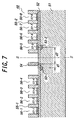
- the first ground electrode and the second ground electrode are divided into plural parts, to fabricate an optical waveguide element 60 as shown in Fig. 7.
- thin films 57-1 through 57-8 are formed at the ditches 56-1 through 56-8, respectively.
- an optical waveguide element In an optical waveguide element according to the present invention, operation point shift due to temperature drift is not caused as the environmental temperature is changed. Therefore, the optical waveguide element can be preferably used for an optical modulator in high velocity and large capacity optical fiber communication system requiring long-term reliability and stability.
- the selectivity of optical fiber can be expanded in its size and figuration for the optical waveguide element.
- an optical modulator able to meet many application can be provided.
Landscapes
- Physics & Mathematics (AREA)
- Nonlinear Science (AREA)
- Electromagnetism (AREA)
- General Physics & Mathematics (AREA)
- Optics & Photonics (AREA)
- Optical Modulation, Optical Deflection, Nonlinear Optics, Optical Demodulation, Optical Logic Elements (AREA)
- Optical Integrated Circuits (AREA)
Abstract
Description
Claims (8)
- An optical waveguide element comprising a substrate made of a material with electro-optical effect, a Mach-Zehnder type optical waveguide formed at the main surface of the substrate, and a modulating electrode to control an optical wave through the Mach-Zehnder type optical waveguide,the Mach-Zehnder type optical waveguide including a first branched optical waveguide and a second branched optical waveguide,the modulating electrode including a signal electrode to modulate an optical wave through the first branched optical waveguide of the Mach-Zehnder type optical waveguide and a ground electrode serving as an opposed electrode for the signal electrode,the ground electrode being composed of a first ground electrode and a second ground electrode which are opposed each other with sandwiching the signal electrode,the first branched optical waveguide being disposed under the signal electrode or in between the first ground electrode and the signal electrode,the second branched optical electrode being disposed under the second ground electrode,the second ground electrode being partially cut away along the long direction and divided, to substantially symmetrize the modulating electrode composed of the signal electrode, the first and the second ground electrodes on the center line between the first and the second branched optical waveguides,the ratio (d2/d1) of the distance d2 between the signal electrode and the second branched optical waveguide to the distance d1 between the signal electrode and the first branched optical waveguide being set within 3.5-7.5.
- An optical waveguide element comprising a substrate made of a material with electro-optical effect, a Mach-Zehnder type optical waveguide formed at the main surface of the substrate, and a modulating electrode to control an optical wave through the Mach-Zehnder type optical waveguide,the Mach-Zehnder type optical waveguide including a first branched optical waveguide and a second branched optical waveguide,the modulating electrode including a signal electrode to modulate an optical wave through the first branched optical waveguide of the Mach-Zehnder type optical waveguide and a ground electrode serving as an opposed electrode for the signal electrode,the ground electrode being composed of a first ground electrode and a second ground electrode which are opposed each other with sandwiching the signal electrode,the first branched optical waveguide being disposed under the signal electrode or in between the first ground electrode and the signal electrode,the second branched optical electrode being disposed under the second ground electrode,the second ground electrode being partially cut away along the long direction and divided, to substantially symmetrize the modulating electrode composed of the signal electrode, the first and the second ground electrodes on the center line between the first and the second branched optical waveguides,the ratio (Ws/Wg) of the width Ws of the signal electrode to the width Wg of the divided part of the second ground electrode located near the signal electrode being set within 0.5-4.
- An optical waveguide element as defined in claim 2, wherein the ratio (d2/d1) of the distance d2 between the signal electrode and the second branched optical waveguide to the distance d1 between the signal electrode and the first branched optical waveguide being set within 3.5-7.5.
- An optical waveguide element comprising a substrate made of a material with electro-optical effect, a Mach-Zehnder type optical waveguide formed at the main surface of the substrate, and a modulating electrode to control an optical wave through the Mach-Zehnder type optical waveguide,the Mach-Zehnder type optical waveguide including a first branched optical waveguide and a second branched optical waveguide,the modulating electrode including a signal electrode to modulate an optical wave through the first branched optical waveguide of the Mach-Zehnder type optical waveguide and a ground electrode serving as an opposed electrode for the signal electrode,the ground electrode being composed of a first ground electrode and a second ground electrode which are opposed each other with sandwiching the signal electrode,the first branched optical waveguide being disposed under the signal electrode or in between the first ground electrode and the signal electrode,the second branched optical electrode being disposed under the second ground electrode,the second ground electrode being partially cut away along the long direction and divided into three parts, the divided first part being disposed on the almost center line between the first and the second branched optical waveguides, the divided second part and the divided third part being almost the same as the signal electrode and the first ground electrode in figuration and dimension, respectively, to substantially symmetrize the modulating electrode composed of the signal electrode, the first and the second ground electrodes on the center line between the first and the second branched optical waveguides,the width W1 of the divided first part being set 0.5-20 times as large as the width Ws of the signal electrode.
- An optical waveguide element as defined in claim 4, wherein the ratio (d2/d1) of the distance d2 between the signal electrode and the second branched optical waveguide to the distance d1 between the signal electrode and the first branched optical waveguide being set within 10-27.
- An optical waveguide element as defined in any one of claims 1-5, wherein a thin film is formed of a conductive material at a ditch formed at the divided second ground electrode.
- An optical waveguide element comprising a substrate made of a material with electro-optical effect, a Mach-Zehnder type optical waveguide formed at the main surface of the substrate, and a modulating electrode to control an optical wave through the Mach-Zehnder type optical waveguide,the Mach-Zehnder type optical waveguide including a first branched optical waveguide and a second branched optical waveguide,the modulating electrode including a signal electrode to modulate an optical wave through the first branched optical waveguide of the Mach-Zehnder type optical waveguide and a ground electrode serving as an opposed electrode for the signal electrode,the ground electrode being composed of a first ground electrode and a second ground electrode which are opposed each other with sandwiching the signal electrode,the first branched optical waveguide being disposed under the signal electrode or in between the first ground electrode and the signal electrode,the second branched optical electrode being disposed under the second ground electrode,the second ground electrode being partially cut away along the long direction and divided, to balance and substantially symmetrize the stresses for the first and the second branched optical waveguides from the modulating electrode composed of the signal electrode, the first and the second ground electrodes on the center line between the first and the second branched optical waveguides.
- An optical waveguide element as defined in any one of claims 1-7, wherein the chirp characteristic is controlled.
Applications Claiming Priority (3)
| Application Number | Priority Date | Filing Date | Title |
|---|---|---|---|
| JP2000064490 | 2000-03-09 | ||
| JP2000064490A JP3362126B2 (en) | 2000-03-09 | 2000-03-09 | Optical waveguide device |
| PCT/JP2001/001688 WO2001067168A1 (en) | 2000-03-09 | 2001-03-05 | Optical waveguide |
Publications (3)
| Publication Number | Publication Date |
|---|---|
| EP1193537A1 true EP1193537A1 (en) | 2002-04-03 |
| EP1193537A4 EP1193537A4 (en) | 2005-03-09 |
| EP1193537B1 EP1193537B1 (en) | 2006-05-31 |
Family
ID=18584187
Family Applications (1)
| Application Number | Title | Priority Date | Filing Date |
|---|---|---|---|
| EP01908311A Expired - Lifetime EP1193537B1 (en) | 2000-03-09 | 2001-03-05 | Optical waveguide |
Country Status (6)
| Country | Link |
|---|---|
| US (2) | US20030007711A1 (en) |
| EP (1) | EP1193537B1 (en) |
| JP (1) | JP3362126B2 (en) |
| CA (1) | CA2373430C (en) |
| DE (1) | DE60120068T2 (en) |
| WO (1) | WO2001067168A1 (en) |
Families Citing this family (8)
| Publication number | Priority date | Publication date | Assignee | Title |
|---|---|---|---|---|
| JP2007264543A (en) * | 2006-03-30 | 2007-10-11 | Fujitsu Ltd | Waveguide type optical device |
| EP2116889B1 (en) | 2007-03-06 | 2014-08-06 | NGK Insulators, Ltd. | Optical phase modulator |
| JP5418222B2 (en) | 2007-03-27 | 2014-02-19 | 富士通株式会社 | Optical device |
| JP5162223B2 (en) * | 2007-08-03 | 2013-03-13 | アンリツ株式会社 | Light modulator |
| JP5010559B2 (en) * | 2007-09-12 | 2012-08-29 | アンリツ株式会社 | Light modulator |
| JP5010408B2 (en) * | 2007-09-14 | 2012-08-29 | アンリツ株式会社 | Light modulator |
| JP5983256B2 (en) * | 2012-09-28 | 2016-08-31 | 住友大阪セメント株式会社 | Light modulator |
| JP5590175B1 (en) * | 2013-03-26 | 2014-09-17 | 住友大阪セメント株式会社 | Light modulator |
Family Cites Families (15)
| Publication number | Priority date | Publication date | Assignee | Title |
|---|---|---|---|---|
| CA2011954C (en) * | 1989-03-14 | 1994-02-22 | Fujitsu Limited | Optical modulator |
| JPH03229215A (en) * | 1990-02-02 | 1991-10-11 | Nippon Telegr & Teleph Corp <Ntt> | Optical modulation element |
| US5138480A (en) * | 1991-08-14 | 1992-08-11 | Hewlett-Packard Company | Traveling wave optical modulator |
| US5303079A (en) * | 1992-04-09 | 1994-04-12 | At&T Bell Laboratories | Tunable chirp, lightwave modulator for dispersion compensation |
| US5291565A (en) * | 1992-06-30 | 1994-03-01 | Hughes Aircraft Company | Broad band, low power electro-optic modulator apparatus and method with segmented electrodes |
| JP3570735B2 (en) * | 1993-02-10 | 2004-09-29 | 住友大阪セメント株式会社 | Optical waveguide device |
| US5388170A (en) | 1993-11-22 | 1995-02-07 | At&T Corp. | Electrooptic device structure and method for reducing thermal effects in optical waveguide modulators |
| JP2825056B2 (en) * | 1994-02-24 | 1998-11-18 | 日本電気株式会社 | Light control device |
| GB9510051D0 (en) * | 1995-05-18 | 1995-07-12 | Integrated Optical Components | Integrated optical modulators |
| JPH0886991A (en) | 1995-10-09 | 1996-04-02 | Fujitsu Ltd | Optical transmission method, optical transmission device, and optical transmission system |
| JP3892928B2 (en) | 1997-02-26 | 2007-03-14 | 花王株式会社 | Process for producing diglycerides and reactor used in the process |
| US6091864A (en) * | 1997-04-10 | 2000-07-18 | Ortel Corporation | Linear optical modulator for providing chirp-free optical signals |
| JPH11237593A (en) * | 1998-02-20 | 1999-08-31 | Sumitomo Osaka Cement Co Ltd | Light modulator |
| JP3660529B2 (en) * | 1999-06-21 | 2005-06-15 | 住友大阪セメント株式会社 | Optical waveguide device |
| US6449080B1 (en) * | 2000-03-08 | 2002-09-10 | Jds Uniphase Corporation | Electro-optic modulator with enhanced bias stability |
-
2000
- 2000-03-09 JP JP2000064490A patent/JP3362126B2/en not_active Expired - Fee Related
-
2001
- 2001-03-05 WO PCT/JP2001/001688 patent/WO2001067168A1/en not_active Ceased
- 2001-03-05 CA CA002373430A patent/CA2373430C/en not_active Expired - Fee Related
- 2001-03-05 US US09/959,857 patent/US20030007711A1/en not_active Abandoned
- 2001-03-05 DE DE60120068T patent/DE60120068T2/en not_active Expired - Lifetime
- 2001-03-05 EP EP01908311A patent/EP1193537B1/en not_active Expired - Lifetime
-
2005
- 2005-02-28 US US11/066,446 patent/US7035488B2/en not_active Expired - Fee Related
Also Published As
| Publication number | Publication date |
|---|---|
| US20030007711A1 (en) | 2003-01-09 |
| EP1193537A4 (en) | 2005-03-09 |
| DE60120068D1 (en) | 2006-07-06 |
| DE60120068T2 (en) | 2006-11-02 |
| US20050157970A1 (en) | 2005-07-21 |
| US7035488B2 (en) | 2006-04-25 |
| EP1193537B1 (en) | 2006-05-31 |
| CA2373430A1 (en) | 2001-09-13 |
| JP3362126B2 (en) | 2003-01-07 |
| WO2001067168A1 (en) | 2001-09-13 |
| JP2001255501A (en) | 2001-09-21 |
| CA2373430C (en) | 2007-07-03 |
Similar Documents
| Publication | Publication Date | Title |
|---|---|---|
| US6334008B2 (en) | Optical circuit and method of fabricating the same | |
| US5278924A (en) | Periodic domain reversal electro-optic modulator | |
| US7693356B2 (en) | Lithium niobate optical modulator | |
| US6501867B2 (en) | Chirp compensated Mach-Zehnder electro-optic modulator | |
| US7400787B2 (en) | Optical modulator with coupled coplanar strip electrode and domain inversion | |
| CN101403840B (en) | External optical modulator with domain inversion for providing constant chirp versus frequency | |
| WO2007111085A1 (en) | Optical waveguide device | |
| EP1020754A1 (en) | Light modulator of waveguide type | |
| US5712933A (en) | Waveguide-type optical device | |
| CA2373430C (en) | An optical waveguide element | |
| JP3660529B2 (en) | Optical waveguide device | |
| JP2002122834A (en) | Optical waveguide element | |
| JP2011100168A (en) | Optical waveguide element | |
| GB2270173A (en) | Optical modulator | |
| JP2836568B2 (en) | Light control element and method of manufacturing the same | |
| JPH0425524B2 (en) | ||
| JP4495326B2 (en) | Chirp control method of light modulation element | |
| JPH06250131A (en) | Light control element | |
| JPS63261220A (en) | Light modulating element | |
| JPH04258918A (en) | Light control circuit | |
| JPH05333296A (en) | Light control element | |
| JP2002049016A (en) | Optical modulator | |
| JPS6150289B2 (en) | ||
| KR19980035328A (en) | Polarization independent electro-optical optical phase modulator and optical switch and optical intensity modulator using the same |
Legal Events
| Date | Code | Title | Description |
|---|---|---|---|
| PUAI | Public reference made under article 153(3) epc to a published international application that has entered the european phase |
Free format text: ORIGINAL CODE: 0009012 |
|
| 17P | Request for examination filed |
Effective date: 20011207 |
|
| AK | Designated contracting states |
Kind code of ref document: A1 Designated state(s): AT BE CH CY DE DK ES FI FR GB GR IE IT LI LU MC NL PT SE TR |
|
| AX | Request for extension of the european patent |
Free format text: AL;LT;LV;MK;RO;SI |
|
| RBV | Designated contracting states (corrected) |
Designated state(s): AT BE CH CY DE FR GB IT LI |
|
| A4 | Supplementary search report drawn up and despatched |
Effective date: 20050124 |
|
| RIC1 | Information provided on ipc code assigned before grant |
Ipc: 7G 02F 1/035 A Ipc: 7G 02F 1/225 B |
|
| 17Q | First examination report despatched |
Effective date: 20050330 |
|
| GRAP | Despatch of communication of intention to grant a patent |
Free format text: ORIGINAL CODE: EPIDOSNIGR1 |
|
| RBV | Designated contracting states (corrected) |
Designated state(s): DE FR GB IT |
|
| GRAS | Grant fee paid |
Free format text: ORIGINAL CODE: EPIDOSNIGR3 |
|
| GRAA | (expected) grant |
Free format text: ORIGINAL CODE: 0009210 |
|
| AK | Designated contracting states |
Kind code of ref document: B1 Designated state(s): DE FR GB IT |
|
| PG25 | Lapsed in a contracting state [announced via postgrant information from national office to epo] |
Ref country code: IT Free format text: LAPSE BECAUSE OF FAILURE TO SUBMIT A TRANSLATION OF THE DESCRIPTION OR TO PAY THE FEE WITHIN THE PRESCRIBED TIME-LIMIT;WARNING: LAPSES OF ITALIAN PATENTS WITH EFFECTIVE DATE BEFORE 2007 MAY HAVE OCCURRED AT ANY TIME BEFORE 2007. THE CORRECT EFFECTIVE DATE MAY BE DIFFERENT FROM THE ONE RECORDED. Effective date: 20060531 |
|
| REG | Reference to a national code |
Ref country code: GB Ref legal event code: FG4D |
|
| REF | Corresponds to: |
Ref document number: 60120068 Country of ref document: DE Date of ref document: 20060706 Kind code of ref document: P |
|
| ET | Fr: translation filed | ||
| PLBE | No opposition filed within time limit |
Free format text: ORIGINAL CODE: 0009261 |
|
| STAA | Information on the status of an ep patent application or granted ep patent |
Free format text: STATUS: NO OPPOSITION FILED WITHIN TIME LIMIT |
|
| 26N | No opposition filed |
Effective date: 20070301 |
|
| PGFP | Annual fee paid to national office [announced via postgrant information from national office to epo] |
Ref country code: GB Payment date: 20100303 Year of fee payment: 10 |
|
| PGFP | Annual fee paid to national office [announced via postgrant information from national office to epo] |
Ref country code: DE Payment date: 20100312 Year of fee payment: 10 |
|
| GBPC | Gb: european patent ceased through non-payment of renewal fee |
Effective date: 20110305 |
|
| PG25 | Lapsed in a contracting state [announced via postgrant information from national office to epo] |
Ref country code: DE Free format text: LAPSE BECAUSE OF NON-PAYMENT OF DUE FEES Effective date: 20111001 |
|
| REG | Reference to a national code |
Ref country code: DE Ref legal event code: R119 Ref document number: 60120068 Country of ref document: DE Effective date: 20111001 |
|
| PG25 | Lapsed in a contracting state [announced via postgrant information from national office to epo] |
Ref country code: GB Free format text: LAPSE BECAUSE OF NON-PAYMENT OF DUE FEES Effective date: 20110305 |
|
| PGFP | Annual fee paid to national office [announced via postgrant information from national office to epo] |
Ref country code: IT Payment date: 20120324 Year of fee payment: 12 |
|
| PGFP | Annual fee paid to national office [announced via postgrant information from national office to epo] |
Ref country code: FR Payment date: 20130325 Year of fee payment: 13 |
|
| REG | Reference to a national code |
Ref country code: FR Ref legal event code: ST Effective date: 20141128 |
|
| PG25 | Lapsed in a contracting state [announced via postgrant information from national office to epo] |
Ref country code: FR Free format text: LAPSE BECAUSE OF NON-PAYMENT OF DUE FEES Effective date: 20140331 |
|
| PG25 | Lapsed in a contracting state [announced via postgrant information from national office to epo] |
Ref country code: IT Free format text: LAPSE BECAUSE OF NON-PAYMENT OF DUE FEES Effective date: 20140305 |